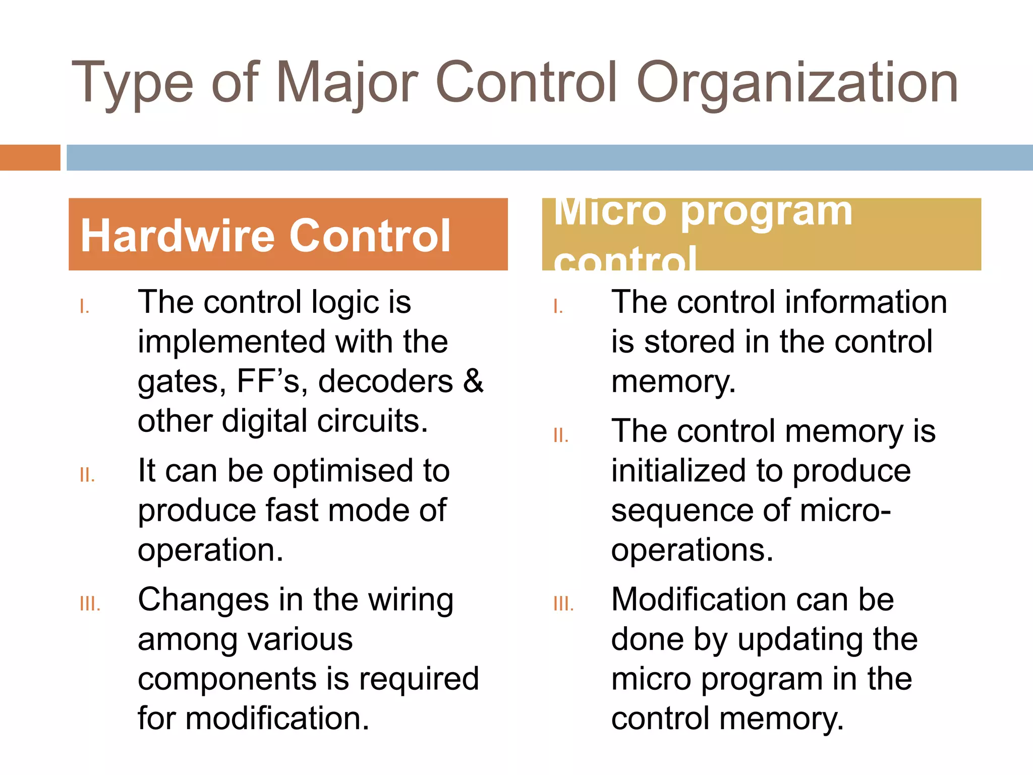
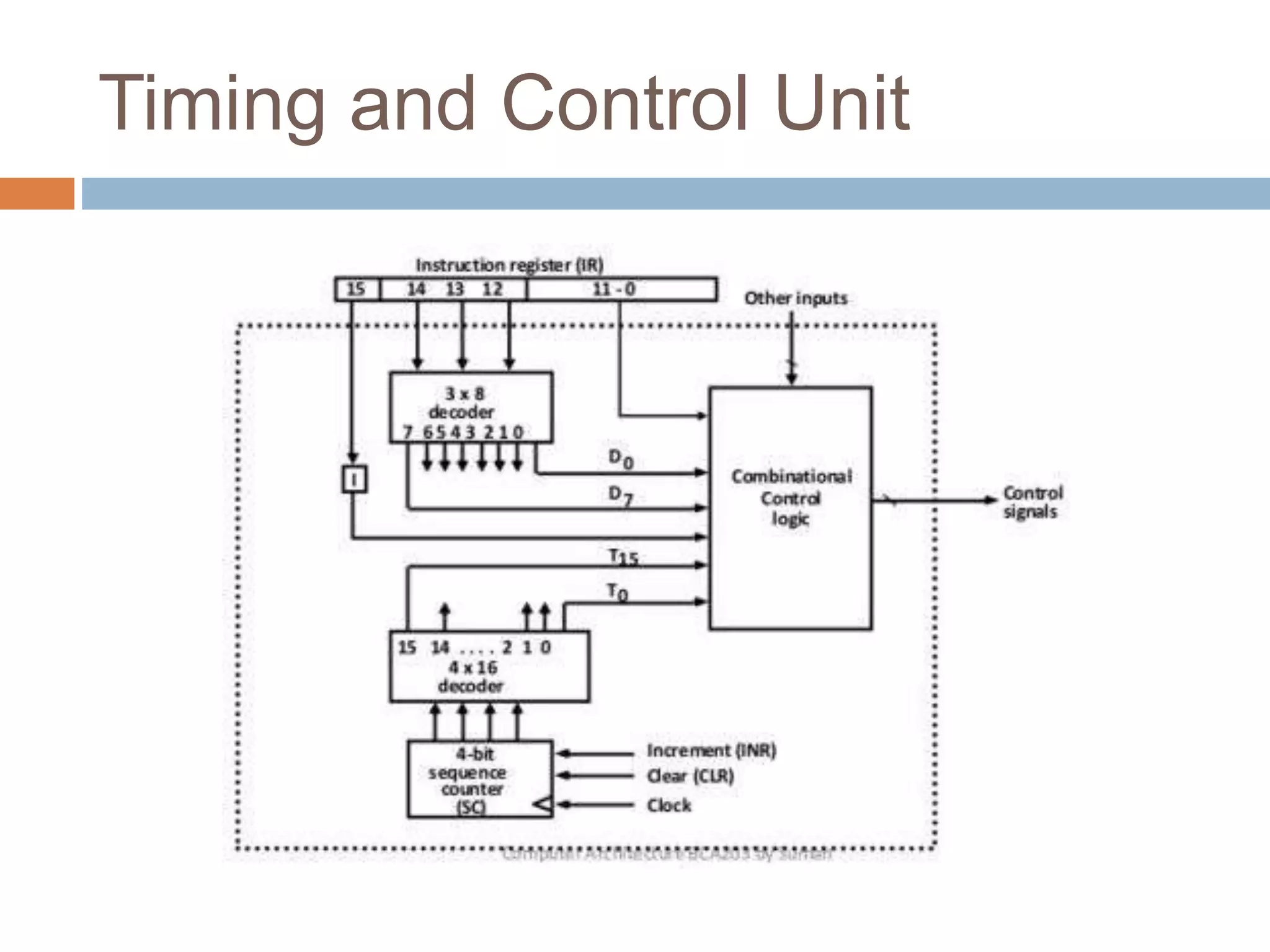
Timing and Control Circuit
 Name- Rajan Shah
Control Unit
 The CPU is partitioned into two parts viz:
1. CU-Control Unit
2. ALU- Arithmetic Logic Unit
 The function of the CU is to generate relevant
timing and control signals to all the operations
in the computer.
 It controls the flow of data between processor,
memory and peripherals.
 CU directs the entire computer system to carry
out stored program instructions.
Timing and Control Signals
 The timing for all the registers in the basic
computer is controlled by the Master Clock
Generator and applied to all the flip-flops and
registers in the system.
 The control signals are generated in control unit
& provide control inputs for the Mux in common
bus, control inputs in the processor register and
micro-operations for accumulator.
Type of Major Control Organization
I. The control logic is
implemented with the
gates, FF’s, decoders &
other digital circuits.
II. It can be optimised to
produce fast mode of
operation.
III. Changes in the wiring
among various
components is required
for modification.
I. The control information
is stored in the control
memory.
II. The control memory is
initialized to produce
sequence of micro-
operations.
III. Modification can be
done by updating the
micro program in the
control memory.
Hardwire Control
Micro program
control
Timing and Control Unit
 A memory read-write cycle will be initiated with
the rising edge of timing signal.
 It will be assumed that a memory cycle time is
less than clock cycle time, according to which
memory cycle will be completed & the clock
transition will be used to load the memory word
into a register.
 Usually wait cycles are provided in the
processor until memory word is available as
memory cycles usually take longer than
processor clock cycle.
Timing Graph
 To understand the operation of basic
computer, it is necessary to understand the
timing relationship between clock transition
and timing signals.
 For E.g.- T0 : AR  PC.
 The above register transfer statement
specifies a transfer of content of PC to AR if
timing signal T0 is active.
 During T0, all the contents of PC are placed
onto bus(S2S1S0 = 010) & LD(load) input of AR
is enabled.
 The transfer doesn’t occur until the end of
clock cycle when a clock goes through a
positive transition and also increments the SC
from 0000 to 0001 which has T0 inactive and
T1 active.
THANK YOU

Timing and control circuit

  • 1.
    Timing and ControlCircuit  Name- Rajan Shah
  • 2.
    Control Unit  TheCPU is partitioned into two parts viz: 1. CU-Control Unit 2. ALU- Arithmetic Logic Unit  The function of the CU is to generate relevant timing and control signals to all the operations in the computer.  It controls the flow of data between processor, memory and peripherals.  CU directs the entire computer system to carry out stored program instructions.
  • 3.
    Timing and ControlSignals  The timing for all the registers in the basic computer is controlled by the Master Clock Generator and applied to all the flip-flops and registers in the system.  The control signals are generated in control unit & provide control inputs for the Mux in common bus, control inputs in the processor register and micro-operations for accumulator.
  • 4.
    Type of MajorControl Organization I. The control logic is implemented with the gates, FF’s, decoders & other digital circuits. II. It can be optimised to produce fast mode of operation. III. Changes in the wiring among various components is required for modification. I. The control information is stored in the control memory. II. The control memory is initialized to produce sequence of micro- operations. III. Modification can be done by updating the micro program in the control memory. Hardwire Control Micro program control
  • 5.
  • 6.
     A memoryread-write cycle will be initiated with the rising edge of timing signal.  It will be assumed that a memory cycle time is less than clock cycle time, according to which memory cycle will be completed & the clock transition will be used to load the memory word into a register.  Usually wait cycles are provided in the processor until memory word is available as memory cycles usually take longer than processor clock cycle.
  • 7.
  • 8.
     To understandthe operation of basic computer, it is necessary to understand the timing relationship between clock transition and timing signals.  For E.g.- T0 : AR  PC.  The above register transfer statement specifies a transfer of content of PC to AR if timing signal T0 is active.  During T0, all the contents of PC are placed onto bus(S2S1S0 = 010) & LD(load) input of AR is enabled.
  • 9.
     The transferdoesn’t occur until the end of clock cycle when a clock goes through a positive transition and also increments the SC from 0000 to 0001 which has T0 inactive and T1 active.
  • 10.