Downloaded 1,796 times


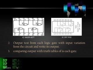


The document discusses logic gates and their circuitry. It describes the 7 main logic gates: NOT, AND, OR, NAND, NOR, XOR, and XNOR. It explains how each gate functions and provides their truth tables. The document then details an experiment where samples of each logic gate integrated circuit were connected in a circuit. The output of each gate was tested with different inputs and compared to their truth tables. It aims to help students understand the components and functionality of logic gates.


![Experimentdsd[1]](https://cdn.slidesharecdn.com/ss_thumbnails/experimentdsd1-121006103055-phpapp01-thumbnail.jpg?width=640&height=640&fit=bounds)


