Download to read offline

![51
flops, Latches and Counters and which themselves can be made by simply connecting together
universal NAND Gates and/or NOR Gates in a particular combinational way to produce the
required sequential circuit.
FLIP-FLOP:-
"Flip-flop" is the common name given to two-state devices which offer basic memory for
sequential logic operations. Flip-flops are heavily used for digital data storage and transfer and
are commonly used in banks called "register" for the storage of binary numerical data.
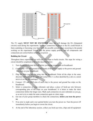
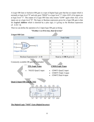
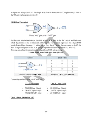
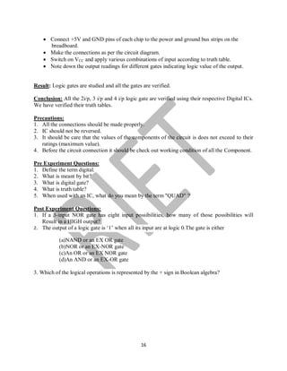
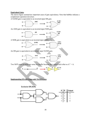
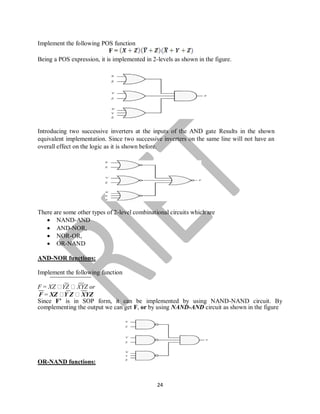
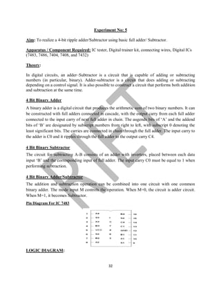
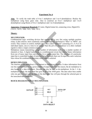
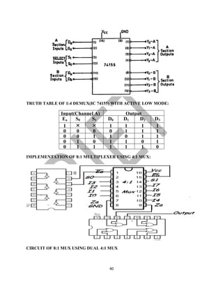
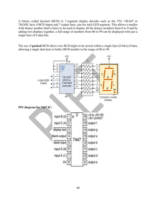
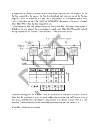
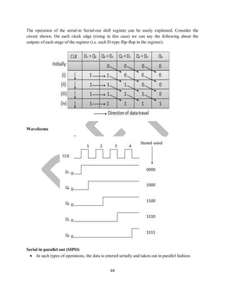
The basic Flip Flop or S-R Flip Flop
The SET-RESET flip flop is designed with the help of two NOR gates and also two NAND
gates. These flip flops are also called S-R Latch.
S-R Flip Flop using NOR Gate
The design of such a flip flop includes two inputs, called the SET [S] and RESET [R]. There are
also two outputs, Q and Q’. The diagram and truth table is shown below.
From the diagram it is evident that the flip flop has mainly four states. They are
S=1, R=0—Q=1, Q’=0
This state is also called the SET state.
S=0, R=1—Q=0, Q’=1
This state is known as the RESET state.
In both the states you can see that the outputs are just compliments of each other and that the
value of Q follows the value of S.
S=0, R=0—Q & Q’ = Remember
If both the values of S and R are switched to 0, then the circuit remembers the value of S and R
in their previous state.
S=1, R=1—Q=0, Q’=0 [Invalid]](https://image.slidesharecdn.com/2thyearivsemdelabmanual-200423142000/85/2th-year-iv-sem-de-lab-manual-51-320.jpg)
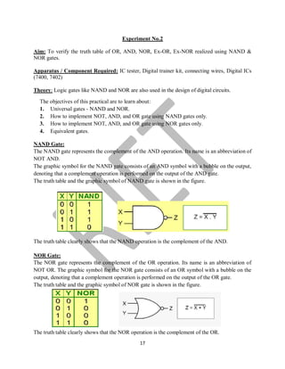
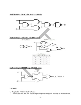
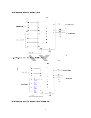
![52
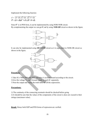
This is an invalid state because the values of both Q and Q’ are 0. They are supposed to be
compliments of each other. Normally, this state must be avoided.
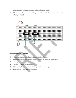
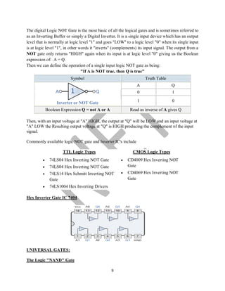
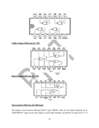
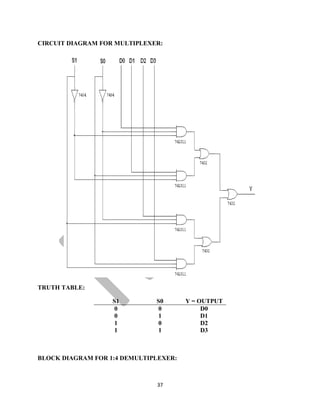
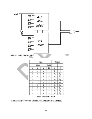
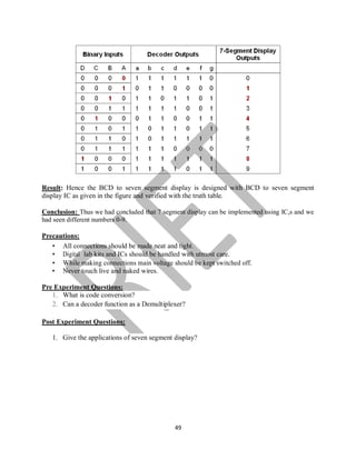
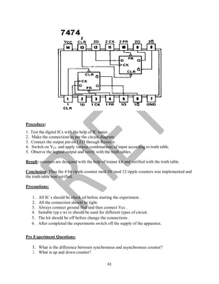
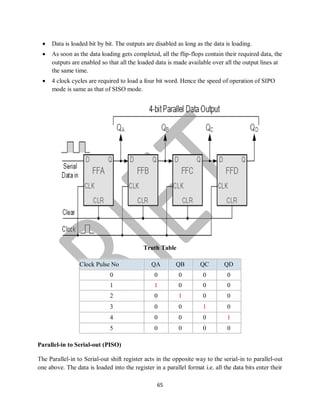
S-R Flip Flop using NAND Gate
The circuit of the S-R flip flop using NAND Gate and its truth table is shown below.
Like the NOR Gate S-R flip flop, this one also has four states. They are
S=1, R=0—Q=0, Q’=1
This state is also called the SET state.
S=0, R=1—Q=1, Q’=0
This state is known as the RESET state.
In both the states you can see that the outputs are just compliments of each other and that the
value of Q follows the compliment value of S.
S=0, R=0—Q=1, & Q’ =1 [Invalid]
If both the values of S and R are switched to 0 it is an invalid state because the values of both Q
and Q’ are 1. They are supposed to be compliments of each other. Normally, this state must be
avoided.
S=1, R=1—Q & Q’= Remember
If both the values of S and R are switched to 1, then the circuit remembers the value of S and R
in their previous state.
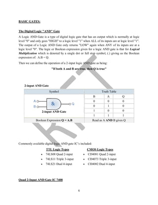
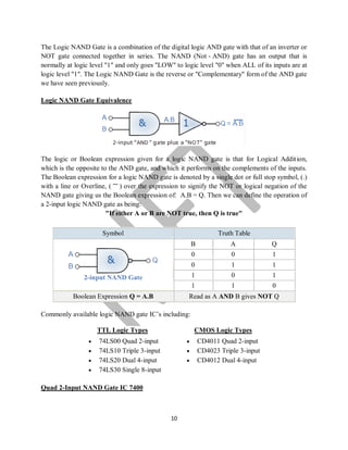
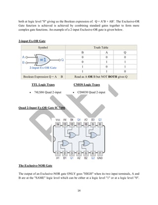
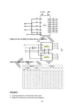
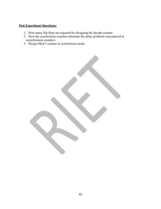
Clocked S-R Flip Flop
It is also called a Gated S-R flip flop.](https://image.slidesharecdn.com/2thyearivsemdelabmanual-200423142000/85/2th-year-iv-sem-de-lab-manual-52-320.jpg)
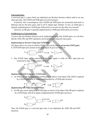
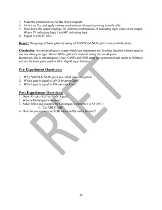
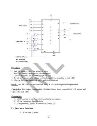
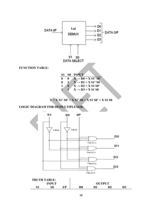
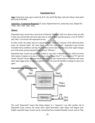
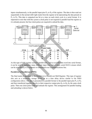
![53
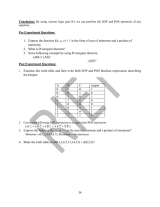
The problems with S-R flip flops using NOR and NAND gate is the invalid state. This problem
can be overcome by using a bistable SR flip-flop that can change outputs when certain invalid
states are met, regardless of the condition of either the Set or the Reset inputs. For this, a clocked
S-R flip flop is designed by adding two AND gates to a basic NOR Gate flip flop. The circuit
diagram and truth table is shown below.
A clock pulse [CP] is given to the inputs of the AND Gate. When the value of the clock pulse is
’0′, the outputs of both the AND Gates remain ’0′. As soon as a pulse is given the value of CP
turns ’1′. This makes the values at S and R to pass through the NOR Gate flip flop. But when the
values of both S and R values turn ’1′, the HIGH value of CP causes both of them to turn to ’0′
for a short moment. As soon as the pulse is removed, the flip flop state becomes intermediate.
Thus either of the two states may be caused, and it depends on whether the set or reset input of
the flip-flop remains a ’1′ longer than the transition to ’0′ at the end of the pulse. Thus the invalid
states can be eliminated.
D Flip Flop
D flip flop is actually a slight modification of the above explained clocked SR flip-flop. From the
figure you can see that the D input is connected to the S input and the complement of the D input
is connected to the R input. The D input is passed on to the flip flop when the value of CP is ’1′.
When CP is HIGH, the flip flop moves to the SET state. If it is ’0′, the flip flop switches to the
CLEAR state.
D Flip Flop without clock
The circuit diagram of D latch with NAND gates:](https://image.slidesharecdn.com/2thyearivsemdelabmanual-200423142000/85/2th-year-iv-sem-de-lab-manual-53-320.jpg)
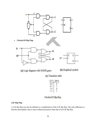
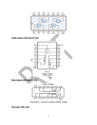
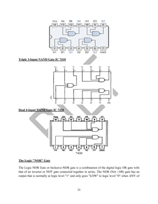
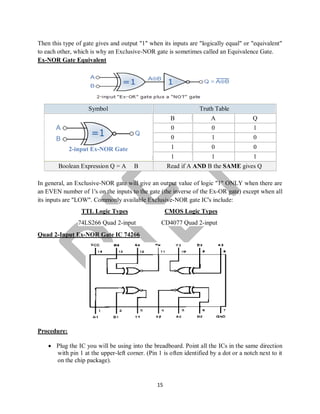
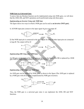
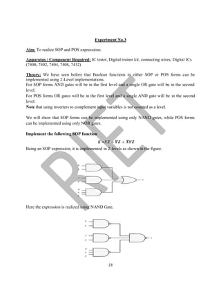
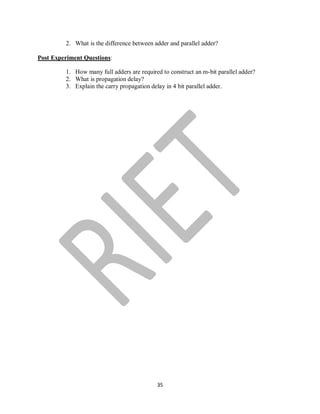
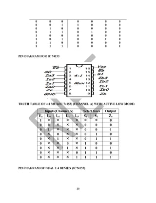
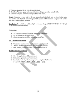
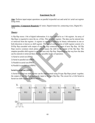
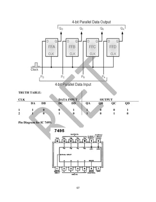
![55
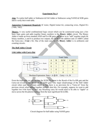
The behavior of inputs J and K is same as the S and R inputs of the S-R flip flop. The letter J
stands for SET and the letter K stands for CLEAR.
JK Flip Flop without clock
When both the inputs J and K have a HIGH state, the flip-flop switches to the complement state.
So, for a value of Q = 1, it switches to Q=0 and for a value of Q = 0, it switches to Q=1.
The circuit diagram and truth-table of a J-K flip flop is shown below.
The circuit includes two 3-input AND gates. The output Q of the flip flop is returned back as a
feedback to the input of the AND along with other inputs like K and clock pulse [CP]. So, if the
value of CP is ’1′, the flip flop gets a CLEAR signal and with the condition that the value of Q
was earlier 1. Similarly output Q’ of the flip flop is given as a feedback to the input of the AND
along with other inputs like J and clock pulse [CP]. So the output becomes SET when the value
of CP is 1 only if the value of Q’ was earlier 1.](https://image.slidesharecdn.com/2thyearivsemdelabmanual-200423142000/85/2th-year-iv-sem-de-lab-manual-55-320.jpg)

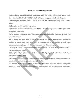
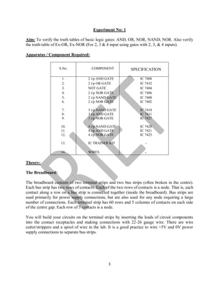
This document provides information about a digital electronics lab manual. It outlines 10 experiments to be performed, including verifying the truth tables of basic logic gates like AND, OR, NAND, and NOR gates. It also describes experiments with half adders, full adders, multiplexers, decoders, flip-flops, and counters. The document provides background information on breadboards and building circuits. It explains the functionality of logic gates like AND, OR, NOT, NAND and NOR gates.