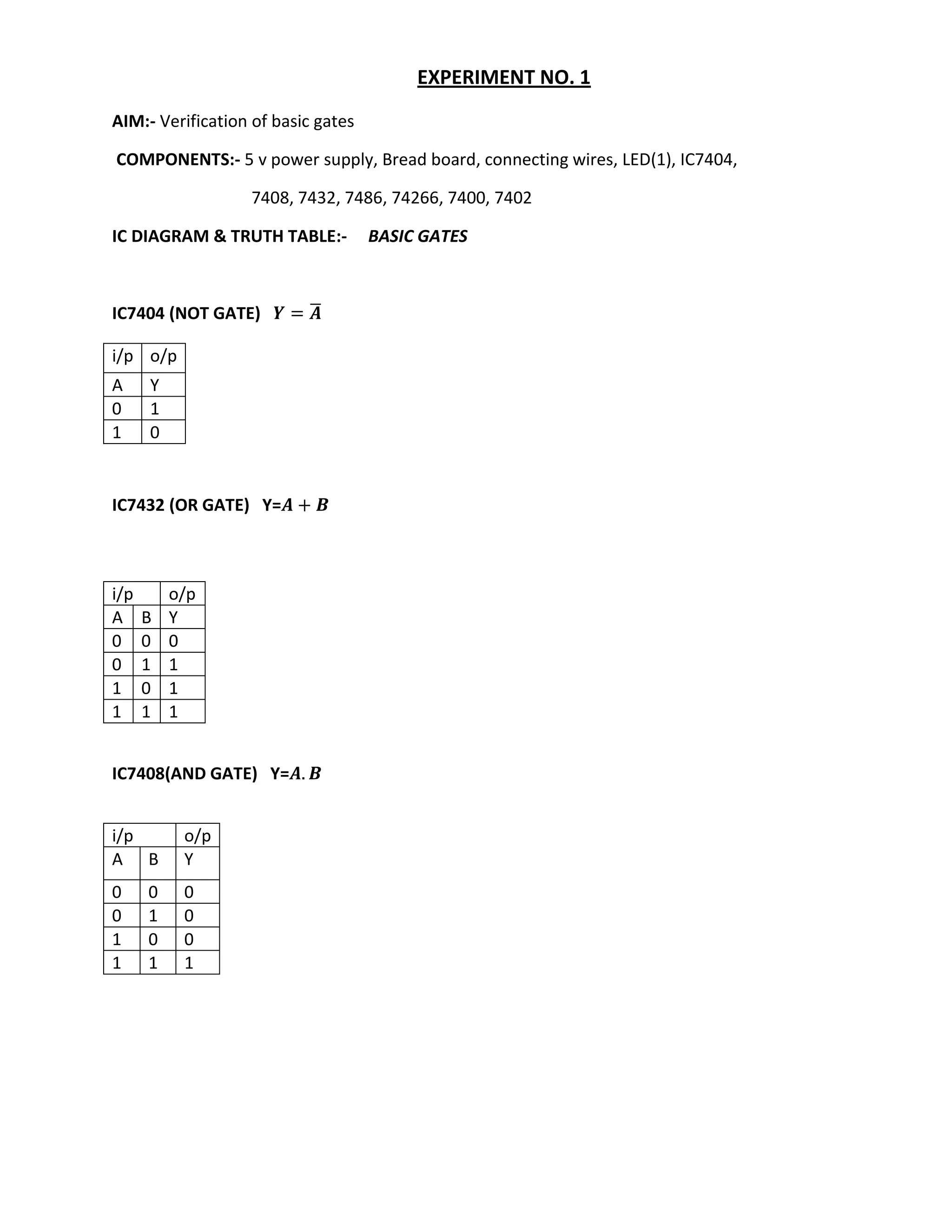
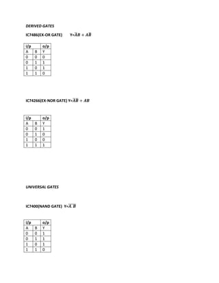
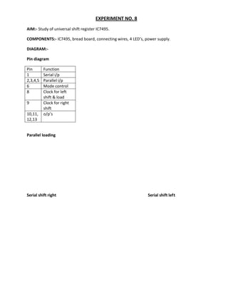
EXPERIMENT NO. 1
AIM:- Verification of basic gates

COMPONENTS:- 5 v power supply, Bread board, connecting wires, LED(1), IC7404,

                  7408, 7432, 7486, 74266, 7400, 7402

IC DIAGRAM & TRUTH TABLE:-          BASIC GATES


IC7404 (NOT GATE)

i/p o/p
A     Y
0     1
1     0


IC7432 (OR GATE) Y=


i/p       o/p
A     B   Y
0     0   0
0     1   1
1     0   1
1     1   1


IC7408(AND GATE) Y=


i/p        o/p
A B        Y
0     0    0
0     1    0
1     0    0
1     1    1
DERIVED GATES

IC7486(EX-OR GATE)     Y=

i/p       o/p
A     B   Y
0     0   0
0     1   1
1     0   1
1     1   0


IC74266(EX-NOR GATE) Y=


i/p       o/p
A     B   Y
0     0   1
0     1   0
1     0   0
1     1   1


UNIVERSAL GATES


IC7400(NAND GATE) Y=


i/p       o/p
A     B   Y
0     0   1
0     1   1
1     0   1
1     1   0
IC7402(NOR GATE) Y=

i/p        o/p
A     B    Y
0     0    1
0     1    0
1     0    0
1     1    0


THEORY:- In digital system there are only few basic operations performed, irrespective of the
complexity of the system . These operations may be required to be performed number of times in a
large digital system like digital computer or digital control systems, etc. The basic operations are AND,
OR, NOT, NAND, NOR, EX-OR, EX-NOR. The circuits which perform these operations are called as
GATEs. These GATEs are basic building blocks for any digital circuit.


PROCEDURE:-1) Connect the IC on the bread board.

                 2) Connect pin no. 7 to ground and pin no. 14 to vcc (5v supply).

                 3) Connect the LED to the o/p pin of a gate.

                 4) give the i/p to the i/p pins of the same gate

                 5) Verify the o/p with respect to the i/p.


RESULT:-


CONCLUSION:-


PRECAUTIONS:- 1) Power supply should not exceeds than 5v.

                    2) Connections should be tight.

                    3) Components should be tested before performing the practical.
EXPERIMENT NO. 2
AIM:- Study of full adder , full substractor and BCD adder

COMPONENTS:- IC 7486, IC7408, IC 7432, IC7404, IC 7410, IC7400, IC7483(2), LED(6), Register(6)470Ω,

                  Bread board, power supply, connecting wires.

DIAGRAM & TRUTH TABLE:-

Full Adder

A   B   Cin   S    Co
0   0   0     0    0
0   0   1     1    0
0   1   0     1    0
0   1   1     0    1
1   0   0     1    0
1   0   1     0    1
1   1   0     0    1
1   1   1     1    1


Full Substractor

A   B   Cin   D    B
0   0   0     0    0
0   0   1     1    1
0   1   0     1    1
0   1   1     0    1
1   0   0     1    0
1   0   1     0    0
1   1   0     0    0
1   1   1     1    1
BCD Adder


THEORY:-


PROCADURE:-1) Mount the ICs on the bread board.

             2) Do the connections for Full adder, substractor, BCD adder.

             3) Apply 5v supply to pin 14 of each IC and connect pin 7 of each IC to ground.

             4) Check the o/p on LED’s and verify the truth table for each ckt.

RESULT:-

CONCLUSION:-

PRECAUTIONS:- 1) Power supply should not exceeds than 5v.

                2) Connections should be tight.

                3) Components should be tested before performing the practical.
EXPERIMENT NO. 3
AIM:- Implementation of Parity checker using gates.

COMPONENTS:- IC7486, LED, register, bread board, connecting wires power supply.

DIAGRAM & TRUTH TABLE:-

input              o/p
P B2    B1   B0    PEO
0 0     0    0     1
0 0     0    1     0
0 0     1    0     0
0 0     1    1     1
0 1     0    0     0
0 1     0    1     1
0 1     1    0     1
0 1     1    1     0
1 0     0    0     0
1 0     0    1     1
1 0     1    0     1
1 0     1    1     0
1 1     0    0     1
1 1     0    1     0
1 1     1    0     0
1 1     1    1     1


THEORY:-

PROCEDURE:- 1) Do the connections as per the ckt. Diagram.

                  2) Give asset of i/p to the ckt.

                  3) Check the error o/p.

                  4) Verify the truth table for ODD parity.

RESULT:-

CONCLUSION:-

PRECAUTIONS:- 1) Power supply should not exceeds than 5v.

                    2) Connections should be tight.

                    3) Components should be tested before performing the practical.
EXPERIMENT NO. 4
AIM:- Implementation of Boolean expression using MUX IC 74153.

               Y=

COMPONENTS:- IC74153, LED, 470Ω register,IC7432, bread board , connecting wires, etc.

DIAGRAM & TRUTH TABLE:-

input        o/p
S3 S2   S1   Y
0 0     0    1
0 0     1    0
0 1     0    1
0 1     1    0
1 0     0    1
1 0     1    0
1 1     0    1
1 1     1    0


THEORY:-

PROCEDURE:- 1) Mount the IC on the bread board.

               2) Do the connections as given in the ckt. Diagram.

               3) Connect pin no. 8 of IC74153 to ground and pin no. 16 to Vcc.

               4) Connect pin no. 7 of IC 7432& IC7404 to ground and pin no. 14 to Vcc.

               5) Give the i/p and verify the o/p .

RESULT:-

CONCLUSION:-

 PRECAUTIONS:- 1) Power supply should not exceeds than 5v.

                   2) Connections should be tight.

                   3) Components should be tested before performing the practical.
EXPERIMENT NO. 5
AIM:- Implement the following function using 4:16 line decoder.

           F 1=                F 1=

COMPONENTS:- IC 74154, 2LED , 2 register 470Ω, 2 IC7432, 2 IC7404, bread board connecting wires.

DIAGRAM:-

input             o/p
A B C        D    F1    F2
0 0 0        0    1     0
0 0 0        1    1     0
0 0 1        0    1     0
0 0 1        1    1     0
0 1 0        0    0     0
0 1 0        1    0     0
0 1 1        0    0     0
0 1 1        1    0     0
1 0 0        0    0     0
1 0 0        1    0     0
1 0 1        0    0     0
1 0 1        1    0     0
1 1 0        0    0     1
1 1 0        1    0     1
1 1 1        0    0     1
1 1 1        1    0     1
THEORY:-

PROCEDURE:- 1) Mount the IC on the bread board. Do the connections as given in the ckt. Diagram

                  2) Connect pin no. 12 of IC74154 to ground and pin no. 24 to Vcc.

                  3) Connect pin no. 7 of IC 7432 & IC7404 to ground and pin no. 14 to Vcc.

                  4) Give the i/p and verify the o/p .

RESULT:-

CONCLUSION:-

PRECAUTIONS:- 1) Power supply should not exceeds than 5v.

                    2) Connections should be tight.

                    3) Components should be tested before performing the practical.
EXPERIMENT NO. 6
AIM:- Conversion of Flip-flop.

COMPONENTS:- 2(IC7400) ,(IC7410),bread board,2 registers, connecting wires,2 LED’s,power supply.

DIAGRAM :-

D FF from SR FF


INPUTS OUTPUTS             COMMENT

E   D      QN+1     QN+1
0   X      QN       QN        NC
1   0      0        1        RESET
1   1      1        0         SET


JK FF from T FF


INPUTS OUTPUTS             COMMENT

E   T      QN+1     QN+1
0   X      QN       QN        NC
1   0      QN       QN        NC
1   1      QN       QN      TOGGLE


THEORY:-

PROCEDURE:-1) Connect the circuit as given in the diagram.

                  2) Apply the inputs and clock input to the circuit.

                  3) Connect the LED to the o/p pin of a gate.

              5) Verify the o/p on LEDs and verify the truth table given.


RESULT:-
EXPERIMENT NO. 7
AIM:- Design decade counter using IC7490.

COMPONENTS:- IC7490, bread board, connecting wires , LED’s 4, power supply.

DIAGRAM & TRUTH TABLE:-

CLK   OA   OB   OC   OD
0     0    0    0    0
1     0    0    0    1
2     0    0    1    0
3     0    0    1    1
4     0    1    0    0
5     0    1    0    1
6     0    1    1    0
7     0    1    1    1
8     1    0    0    0
9     1    0    0    1
10    1    0    1    0
11    1    0    1    1


THEORY:-


PROCEDURE:- 1) Mount the IC 7490 on the bread board.

                2) Do the connections as given in the diagram.

                3) Check the sequence generated by counter & verify the truth table.

RESULT:-


CONCLUSION:-


PRECAUTIONS:- 1) Power supply should not exceeds than 5v.

                  2) Connections should be tight.

                  3) Components should be tested before performing the practical.
EXPERIMENT NO. 8
AIM:- Study of universal shift register IC7495.

COMPONENTS:- IC7495, bread board, connecting wires, 4 LED’s, power supply.

DIAGRAM:-

Pin diagram

Pin       Function
1         Serial i/p
2,3,4,5   Parallel i/p
6         Mode control
8         Clock for left
          shift & load
9         Clock for right
          shift
10,11,    o/p’s
12,13


Parallel loading


Serial shift right                                            Serial shift left
THEORY:-


PROCEDURE:- 1) Connect the IC 7495 on the bread board.

             2) Give clock from function generator.

             3) Do the connections for the register in different modes one by one and check the

                 o/p on LED’s.


RESULT:-


CONCLUSION:-


PRECAUTIONS:- 1) Power supply should not exceeds than 5v.

                2) Connections should be tight.

                3) Components should be tested before performing the practical.

CONCLUSION:-


PRECAUTIONS:- 1) Power supply should not exceeds than 5v.

                2) Connections should be tight.

                3) Components should be tested before performing the practical.
ATHARVA COLLEGE OF ENGG.

                          DEPARTMENT OF ELECTRONICS ENGG.


                        SUB:- DIGITAL SYSTEM DESIGN

                            LIST OF EXPERIMENT

1) Verification of basic gates

2) Study of full adder , full substractor and BCD adder

3) Implementation of Parity checker using gates.

4) Implementation of Boolean expression using MUX IC 74153.

                  Y=

5) Implement the following function using 4:16 line decoder.

            F1=

6) Convert SR FF into JK, D and T FF

7) Design decade counter using IC7490.

8) Study of universal shift register IC7495.


                                            Mr.zafar khan

                                            (Subject in charge DSD-1)
Experimentdsd[1]

Experimentdsd[1]

  • 1.
    EXPERIMENT NO. 1 AIM:-Verification of basic gates COMPONENTS:- 5 v power supply, Bread board, connecting wires, LED(1), IC7404, 7408, 7432, 7486, 74266, 7400, 7402 IC DIAGRAM & TRUTH TABLE:- BASIC GATES IC7404 (NOT GATE) i/p o/p A Y 0 1 1 0 IC7432 (OR GATE) Y= i/p o/p A B Y 0 0 0 0 1 1 1 0 1 1 1 1 IC7408(AND GATE) Y= i/p o/p A B Y 0 0 0 0 1 0 1 0 0 1 1 1
  • 2.
    DERIVED GATES IC7486(EX-OR GATE) Y= i/p o/p A B Y 0 0 0 0 1 1 1 0 1 1 1 0 IC74266(EX-NOR GATE) Y= i/p o/p A B Y 0 0 1 0 1 0 1 0 0 1 1 1 UNIVERSAL GATES IC7400(NAND GATE) Y= i/p o/p A B Y 0 0 1 0 1 1 1 0 1 1 1 0
  • 3.
    IC7402(NOR GATE) Y= i/p o/p A B Y 0 0 1 0 1 0 1 0 0 1 1 0 THEORY:- In digital system there are only few basic operations performed, irrespective of the complexity of the system . These operations may be required to be performed number of times in a large digital system like digital computer or digital control systems, etc. The basic operations are AND, OR, NOT, NAND, NOR, EX-OR, EX-NOR. The circuits which perform these operations are called as GATEs. These GATEs are basic building blocks for any digital circuit. PROCEDURE:-1) Connect the IC on the bread board. 2) Connect pin no. 7 to ground and pin no. 14 to vcc (5v supply). 3) Connect the LED to the o/p pin of a gate. 4) give the i/p to the i/p pins of the same gate 5) Verify the o/p with respect to the i/p. RESULT:- CONCLUSION:- PRECAUTIONS:- 1) Power supply should not exceeds than 5v. 2) Connections should be tight. 3) Components should be tested before performing the practical.
  • 4.
    EXPERIMENT NO. 2 AIM:-Study of full adder , full substractor and BCD adder COMPONENTS:- IC 7486, IC7408, IC 7432, IC7404, IC 7410, IC7400, IC7483(2), LED(6), Register(6)470Ω, Bread board, power supply, connecting wires. DIAGRAM & TRUTH TABLE:- Full Adder A B Cin S Co 0 0 0 0 0 0 0 1 1 0 0 1 0 1 0 0 1 1 0 1 1 0 0 1 0 1 0 1 0 1 1 1 0 0 1 1 1 1 1 1 Full Substractor A B Cin D B 0 0 0 0 0 0 0 1 1 1 0 1 0 1 1 0 1 1 0 1 1 0 0 1 0 1 0 1 0 0 1 1 0 0 0 1 1 1 1 1
  • 5.
    BCD Adder THEORY:- PROCADURE:-1) Mountthe ICs on the bread board. 2) Do the connections for Full adder, substractor, BCD adder. 3) Apply 5v supply to pin 14 of each IC and connect pin 7 of each IC to ground. 4) Check the o/p on LED’s and verify the truth table for each ckt. RESULT:- CONCLUSION:- PRECAUTIONS:- 1) Power supply should not exceeds than 5v. 2) Connections should be tight. 3) Components should be tested before performing the practical.
  • 6.
    EXPERIMENT NO. 3 AIM:-Implementation of Parity checker using gates. COMPONENTS:- IC7486, LED, register, bread board, connecting wires power supply. DIAGRAM & TRUTH TABLE:- input o/p P B2 B1 B0 PEO 0 0 0 0 1 0 0 0 1 0 0 0 1 0 0 0 0 1 1 1 0 1 0 0 0 0 1 0 1 1 0 1 1 0 1 0 1 1 1 0 1 0 0 0 0 1 0 0 1 1 1 0 1 0 1 1 0 1 1 0 1 1 0 0 1 1 1 0 1 0 1 1 1 0 0 1 1 1 1 1 THEORY:- PROCEDURE:- 1) Do the connections as per the ckt. Diagram. 2) Give asset of i/p to the ckt. 3) Check the error o/p. 4) Verify the truth table for ODD parity. RESULT:- CONCLUSION:- PRECAUTIONS:- 1) Power supply should not exceeds than 5v. 2) Connections should be tight. 3) Components should be tested before performing the practical.
  • 7.
    EXPERIMENT NO. 4 AIM:-Implementation of Boolean expression using MUX IC 74153. Y= COMPONENTS:- IC74153, LED, 470Ω register,IC7432, bread board , connecting wires, etc. DIAGRAM & TRUTH TABLE:- input o/p S3 S2 S1 Y 0 0 0 1 0 0 1 0 0 1 0 1 0 1 1 0 1 0 0 1 1 0 1 0 1 1 0 1 1 1 1 0 THEORY:- PROCEDURE:- 1) Mount the IC on the bread board. 2) Do the connections as given in the ckt. Diagram. 3) Connect pin no. 8 of IC74153 to ground and pin no. 16 to Vcc. 4) Connect pin no. 7 of IC 7432& IC7404 to ground and pin no. 14 to Vcc. 5) Give the i/p and verify the o/p . RESULT:- CONCLUSION:- PRECAUTIONS:- 1) Power supply should not exceeds than 5v. 2) Connections should be tight. 3) Components should be tested before performing the practical.
  • 8.
    EXPERIMENT NO. 5 AIM:-Implement the following function using 4:16 line decoder. F 1= F 1= COMPONENTS:- IC 74154, 2LED , 2 register 470Ω, 2 IC7432, 2 IC7404, bread board connecting wires. DIAGRAM:- input o/p A B C D F1 F2 0 0 0 0 1 0 0 0 0 1 1 0 0 0 1 0 1 0 0 0 1 1 1 0 0 1 0 0 0 0 0 1 0 1 0 0 0 1 1 0 0 0 0 1 1 1 0 0 1 0 0 0 0 0 1 0 0 1 0 0 1 0 1 0 0 0 1 0 1 1 0 0 1 1 0 0 0 1 1 1 0 1 0 1 1 1 1 0 0 1 1 1 1 1 0 1 THEORY:- PROCEDURE:- 1) Mount the IC on the bread board. Do the connections as given in the ckt. Diagram 2) Connect pin no. 12 of IC74154 to ground and pin no. 24 to Vcc. 3) Connect pin no. 7 of IC 7432 & IC7404 to ground and pin no. 14 to Vcc. 4) Give the i/p and verify the o/p . RESULT:- CONCLUSION:- PRECAUTIONS:- 1) Power supply should not exceeds than 5v. 2) Connections should be tight. 3) Components should be tested before performing the practical.
  • 9.
    EXPERIMENT NO. 6 AIM:-Conversion of Flip-flop. COMPONENTS:- 2(IC7400) ,(IC7410),bread board,2 registers, connecting wires,2 LED’s,power supply. DIAGRAM :- D FF from SR FF INPUTS OUTPUTS COMMENT E D QN+1 QN+1 0 X QN QN NC 1 0 0 1 RESET 1 1 1 0 SET JK FF from T FF INPUTS OUTPUTS COMMENT E T QN+1 QN+1 0 X QN QN NC 1 0 QN QN NC 1 1 QN QN TOGGLE THEORY:- PROCEDURE:-1) Connect the circuit as given in the diagram. 2) Apply the inputs and clock input to the circuit. 3) Connect the LED to the o/p pin of a gate. 5) Verify the o/p on LEDs and verify the truth table given. RESULT:-
  • 10.
    EXPERIMENT NO. 7 AIM:-Design decade counter using IC7490. COMPONENTS:- IC7490, bread board, connecting wires , LED’s 4, power supply. DIAGRAM & TRUTH TABLE:- CLK OA OB OC OD 0 0 0 0 0 1 0 0 0 1 2 0 0 1 0 3 0 0 1 1 4 0 1 0 0 5 0 1 0 1 6 0 1 1 0 7 0 1 1 1 8 1 0 0 0 9 1 0 0 1 10 1 0 1 0 11 1 0 1 1 THEORY:- PROCEDURE:- 1) Mount the IC 7490 on the bread board. 2) Do the connections as given in the diagram. 3) Check the sequence generated by counter & verify the truth table. RESULT:- CONCLUSION:- PRECAUTIONS:- 1) Power supply should not exceeds than 5v. 2) Connections should be tight. 3) Components should be tested before performing the practical.
  • 11.
    EXPERIMENT NO. 8 AIM:-Study of universal shift register IC7495. COMPONENTS:- IC7495, bread board, connecting wires, 4 LED’s, power supply. DIAGRAM:- Pin diagram Pin Function 1 Serial i/p 2,3,4,5 Parallel i/p 6 Mode control 8 Clock for left shift & load 9 Clock for right shift 10,11, o/p’s 12,13 Parallel loading Serial shift right Serial shift left
  • 12.
    THEORY:- PROCEDURE:- 1) Connectthe IC 7495 on the bread board. 2) Give clock from function generator. 3) Do the connections for the register in different modes one by one and check the o/p on LED’s. RESULT:- CONCLUSION:- PRECAUTIONS:- 1) Power supply should not exceeds than 5v. 2) Connections should be tight. 3) Components should be tested before performing the practical. CONCLUSION:- PRECAUTIONS:- 1) Power supply should not exceeds than 5v. 2) Connections should be tight. 3) Components should be tested before performing the practical.
  • 13.
    ATHARVA COLLEGE OFENGG. DEPARTMENT OF ELECTRONICS ENGG. SUB:- DIGITAL SYSTEM DESIGN LIST OF EXPERIMENT 1) Verification of basic gates 2) Study of full adder , full substractor and BCD adder 3) Implementation of Parity checker using gates. 4) Implementation of Boolean expression using MUX IC 74153. Y= 5) Implement the following function using 4:16 line decoder. F1= 6) Convert SR FF into JK, D and T FF 7) Design decade counter using IC7490. 8) Study of universal shift register IC7495. Mr.zafar khan (Subject in charge DSD-1)