Downloaded 244 times
![Transmitter Output Power
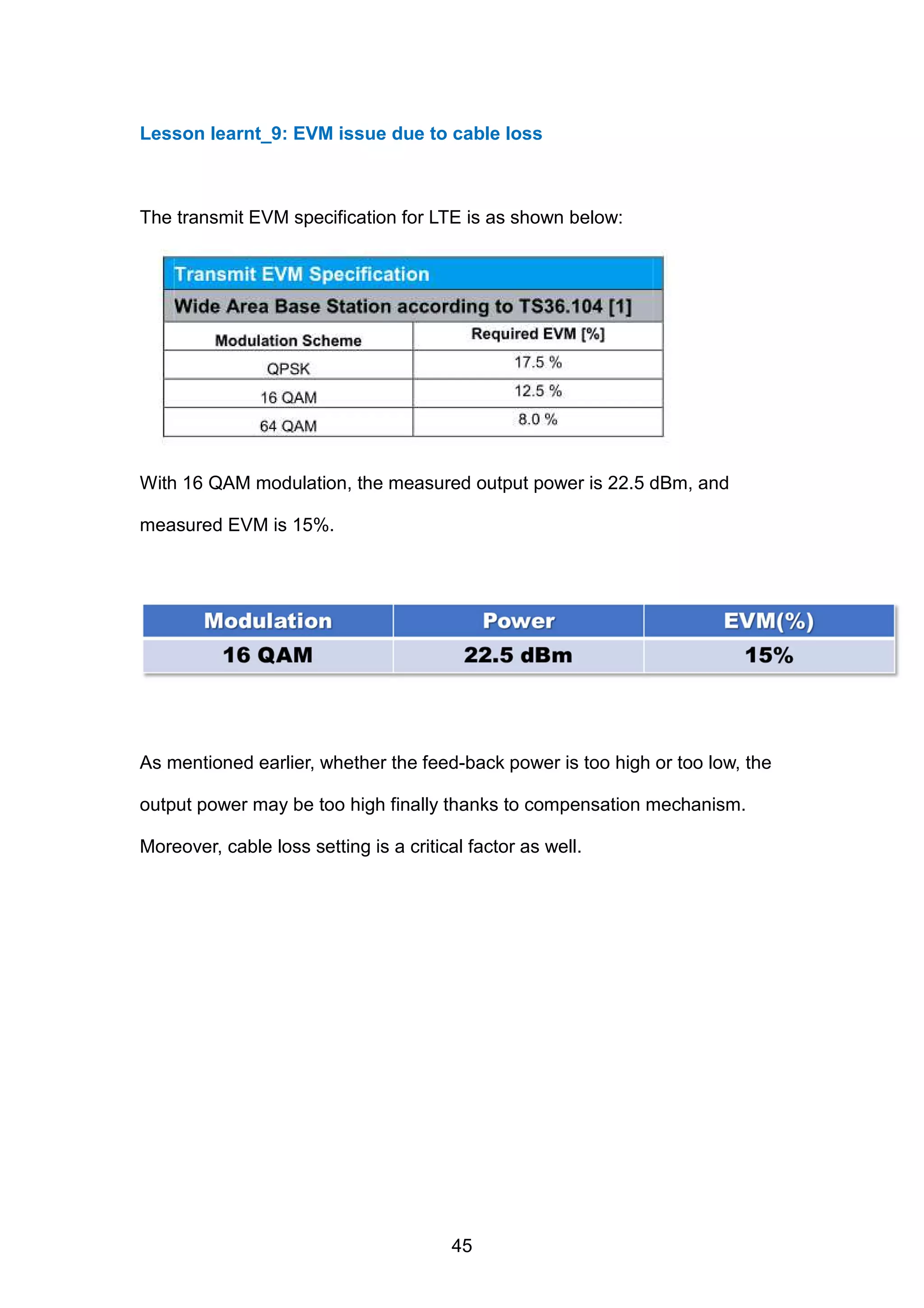
The LTE specified maximum output power:23 dBm with a tolerance of ± 2
dB [1,6].
Nevertheless, the WCDMA specified 24 dBm with a tolerance of +1/−3 dB [1].
The overall LTE key parameters are shown below [2]:
1](https://image.slidesharecdn.com/performancerequirementandlessonslearntoflteterminaltransmitterpart-190106204811/75/Performance-Requirement-and-Lessons-Learnt-of-LTE-Terminal_Transmitter-Part-1-2048.jpg)
![LTE makes use of QPSK, 16QAM, and 64QAM for uplink transmission, but
WCDMA makes use of BPSK for uplink transmission. The overall bits per
symbol table for these modulation types is summarized as below [3]:
BPSK makes use of two symbols, which is two to the first power. So the bits
per symbol is one; QPSK makes use of four symbols, which is two squared.
So the bits per symbol is two; 64QAM makes use of sixty-four symbols, which
is two to the sixth power. So the bits per symbol is six, and so on [4].
2](https://image.slidesharecdn.com/performancerequirementandlessonslearntoflteterminaltransmitterpart-190106204811/75/Performance-Requirement-and-Lessons-Learnt-of-LTE-Terminal_Transmitter-Part-2-2048.jpg)
![Higher order modulation achieves higher data rate, but at the expense of
higher PAR (Peak -to-Average-Ratio), which requires more back-off to retain
linearity [1,5].
3](https://image.slidesharecdn.com/performancerequirementandlessonslearntoflteterminaltransmitterpart-190106204811/75/Performance-Requirement-and-Lessons-Learnt-of-LTE-Terminal_Transmitter-Part-3-2048.jpg)
![SC-FDMA is used for LTE uplink transmission to reduce PAR [5].
Nevertheless, LTE still has higher PAR in uplink modulation than WCDMA. [1]
Thus, that’s why maximum output power of LTE is 23 dBm, but 24 dBm of
WCDMA.
Furthermore, MPR (Maximum Power Reduction) has been introduced in LTE
to take into account the higher PAR of 16QAM modulation and RB (Resource
Block) allocation [1,6]. That’s why the output power is lower under full RBs.
5](https://image.slidesharecdn.com/performancerequirementandlessonslearntoflteterminaltransmitterpart-190106204811/75/Performance-Requirement-and-Lessons-Learnt-of-LTE-Terminal_Transmitter-Part-5-2048.jpg)
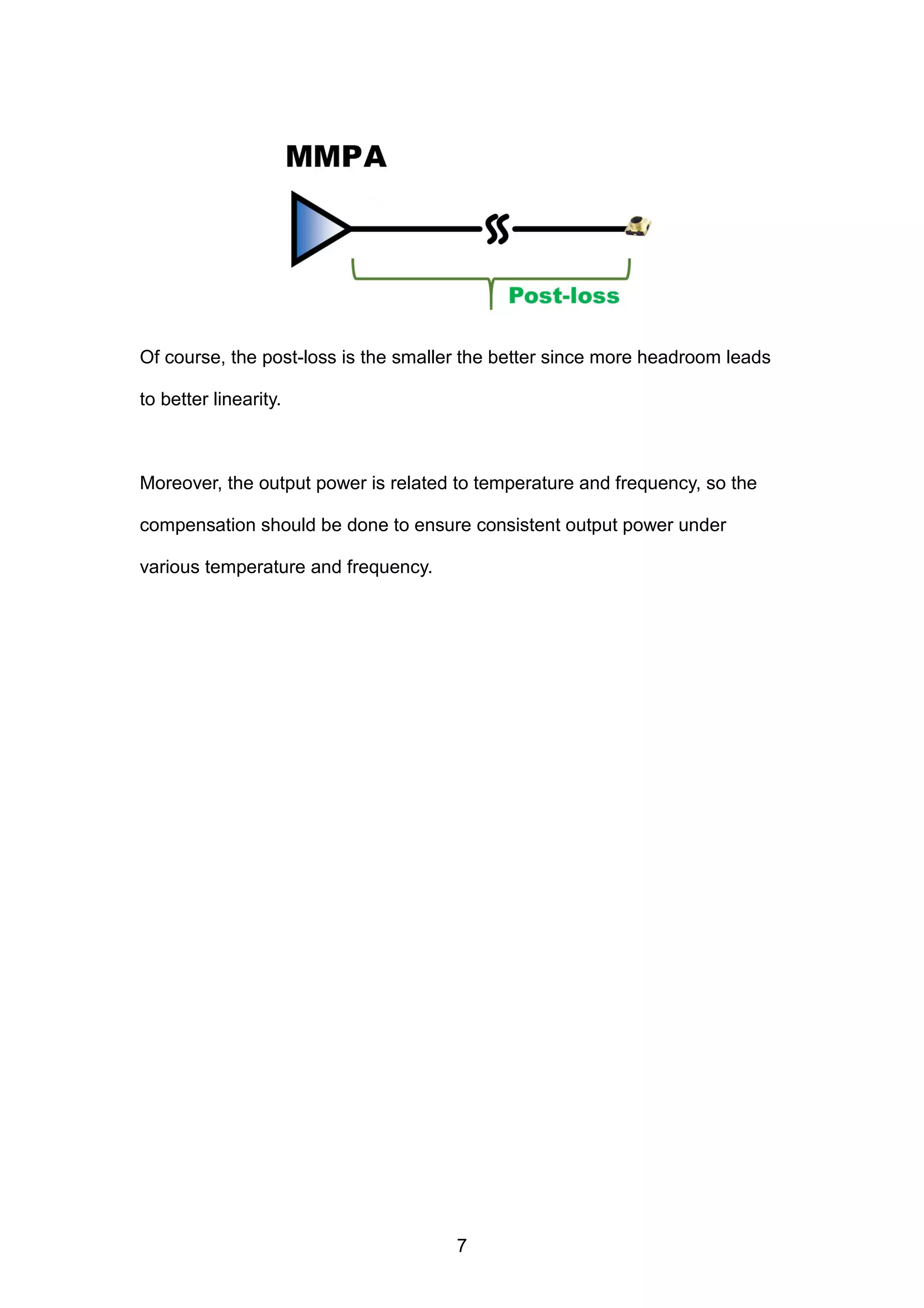
![LTE power control ranges from -40 dBm to 23 dBm. [1]
Take SKYWORKS SKY77645-11 for example, its maximum power in LTE B7
is 28.5 dBm, which indicates the MMPA post-loss should be less than 5.5 dB.
6](https://image.slidesharecdn.com/performancerequirementandlessonslearntoflteterminaltransmitterpart-190106204811/75/Performance-Requirement-and-Lessons-Learnt-of-LTE-Terminal_Transmitter-Part-6-2048.jpg)
![As for power control, Qualcomm makes use of FBRX (Feedback Receiver)
method:
As shown above, the output power is usually coupled back to transceiver by
means of the coupler integrated in ASM (Antenna Switch Module). Take
SKYWORKS SKY77912-11 for example [9]
Thus, the overall process is closed loop, thereby adjusting output power by
the feedback power to retain accuracy.
9](https://image.slidesharecdn.com/performancerequirementandlessonslearntoflteterminaltransmitterpart-190106204811/75/Performance-Requirement-and-Lessons-Learnt-of-LTE-Terminal_Transmitter-Part-9-2048.jpg)
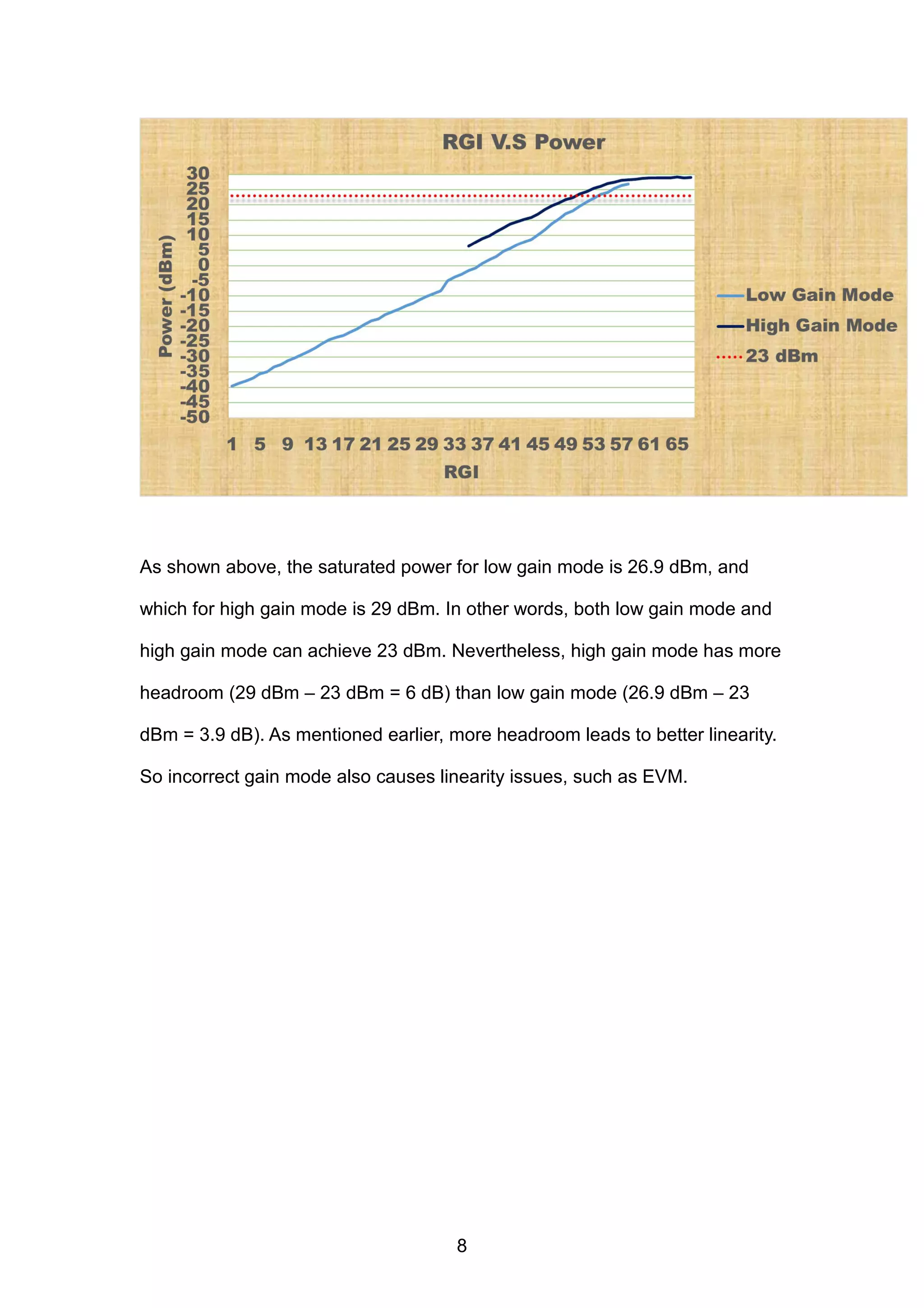
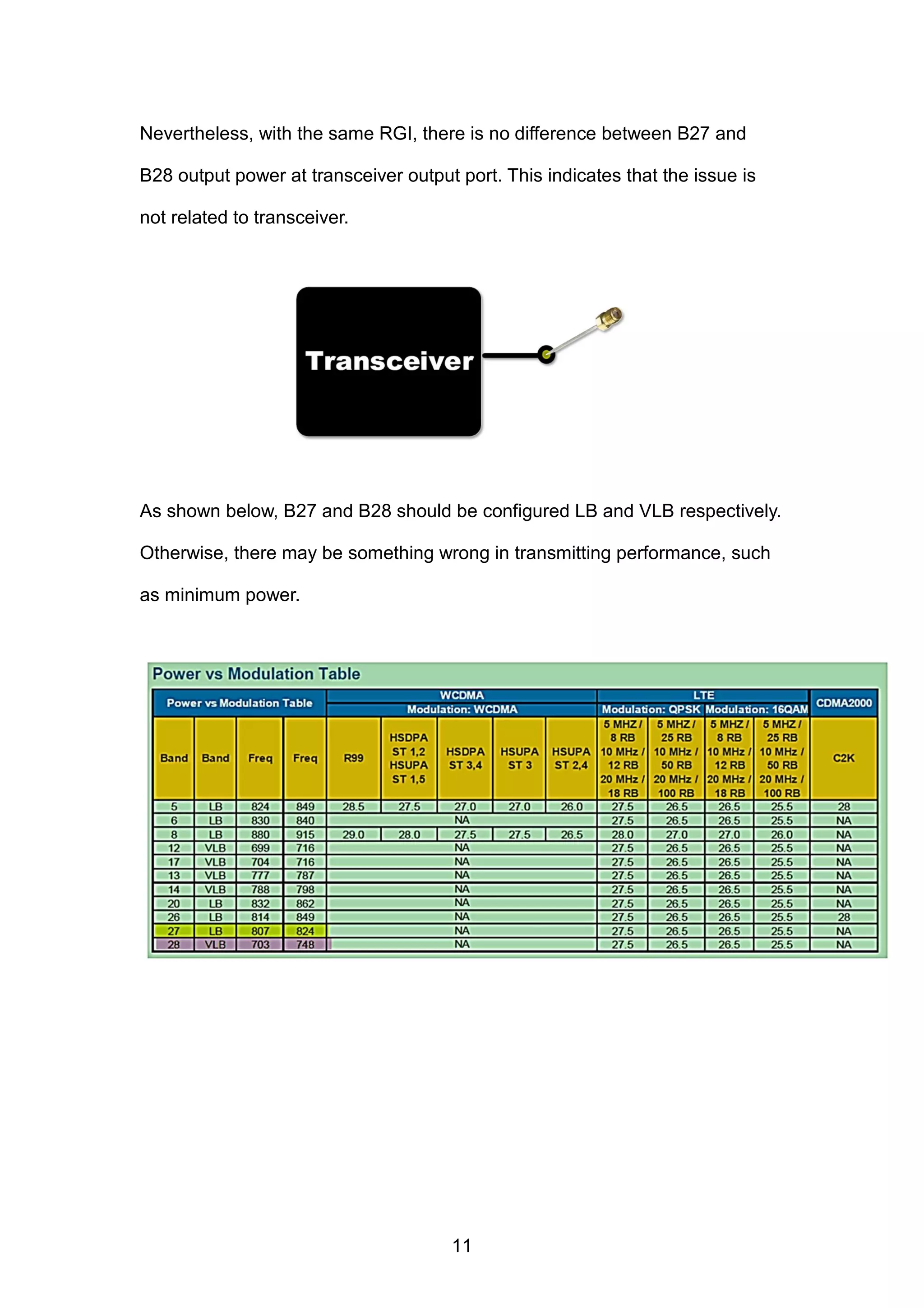
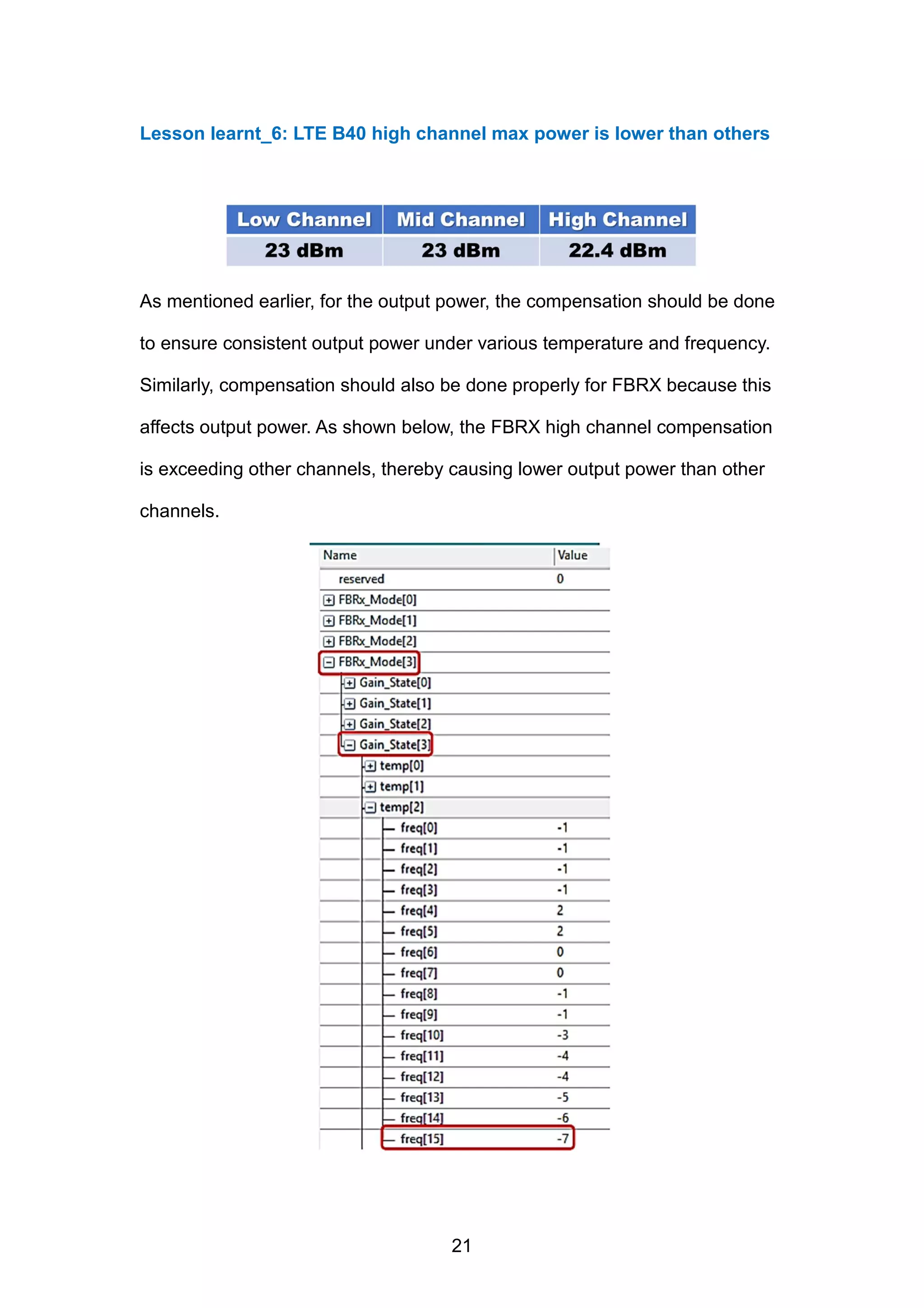
![Lesson learnt_1: B28 Minimum power issue
While doing minimum power measurement, B27 can achieve the power level
less than -30 dBm, but B28 can NOT [10]. Additionally, as shown below,
B27/B28 share the identical transmitting path. In other words, the issue is not
due to hardware issue since B27 is normal. While doing calibration, with the
identical RGI (RF Gain Index), there is approximately 10 dB gap between B27
and B28, as shown below [10]:
10](https://image.slidesharecdn.com/performancerequirementandlessonslearntoflteterminaltransmitterpart-190106204811/75/Performance-Requirement-and-Lessons-Learnt-of-LTE-Terminal_Transmitter-Part-10-2048.jpg)
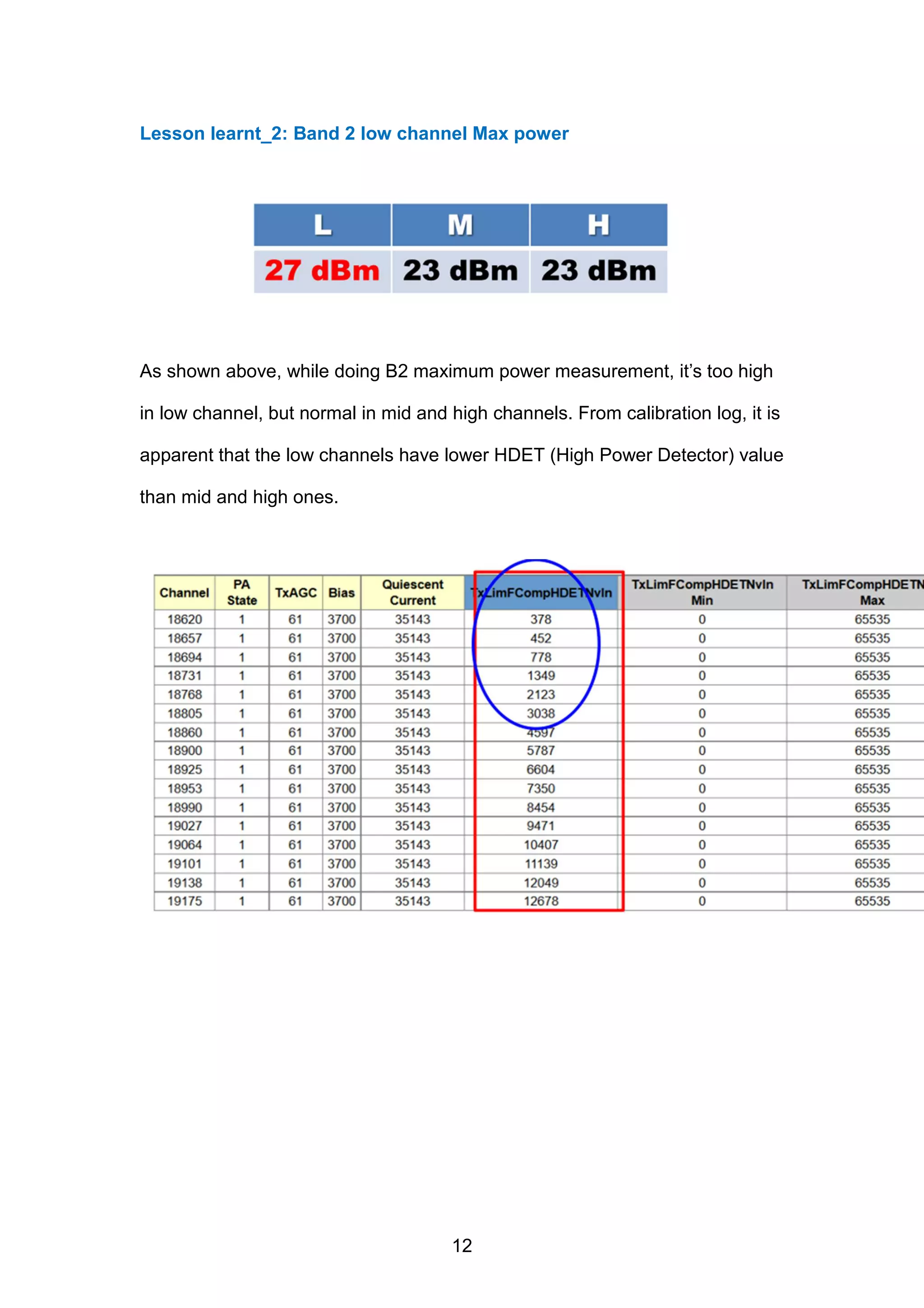
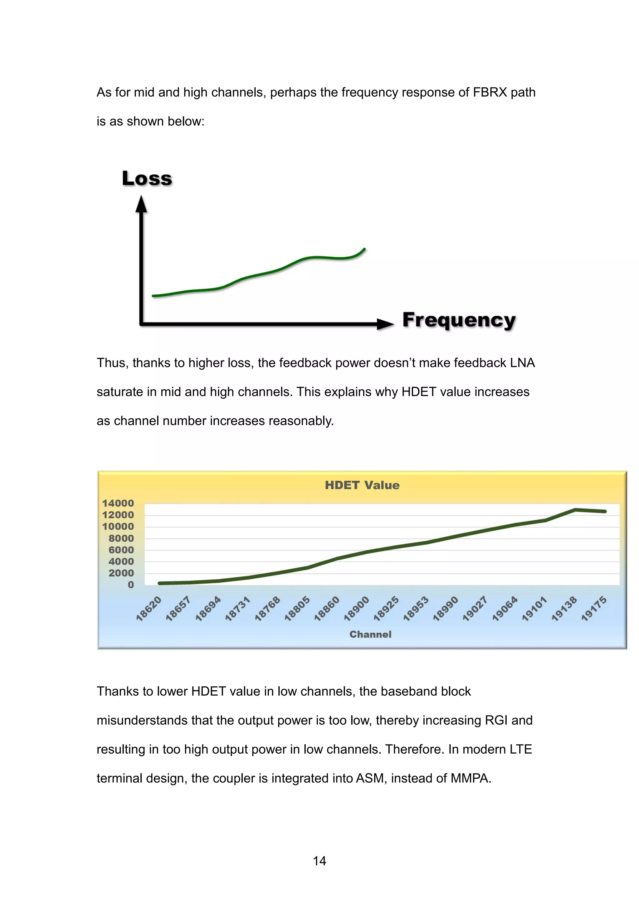
![As shown above, the measured maximum power at connector should be 23
dBm. We assume the loss of duplexer is approximately 3 dB, so the output
power at MMPA is 26 dBm. Because the coupler is integrated into MMPA and
the coupling factor is 23 dB, the feedback power is 3 dBm, which is higher
than the handling capacity of feedback LNA. As shown below, with a strong
input signal, the gain of LNA reduces [11]. That’s why the low channels have
lower HDET value than mid and high ones.
13](https://image.slidesharecdn.com/performancerequirementandlessonslearntoflteterminaltransmitterpart-190106204811/75/Performance-Requirement-and-Lessons-Learnt-of-LTE-Terminal_Transmitter-Part-13-2048.jpg)
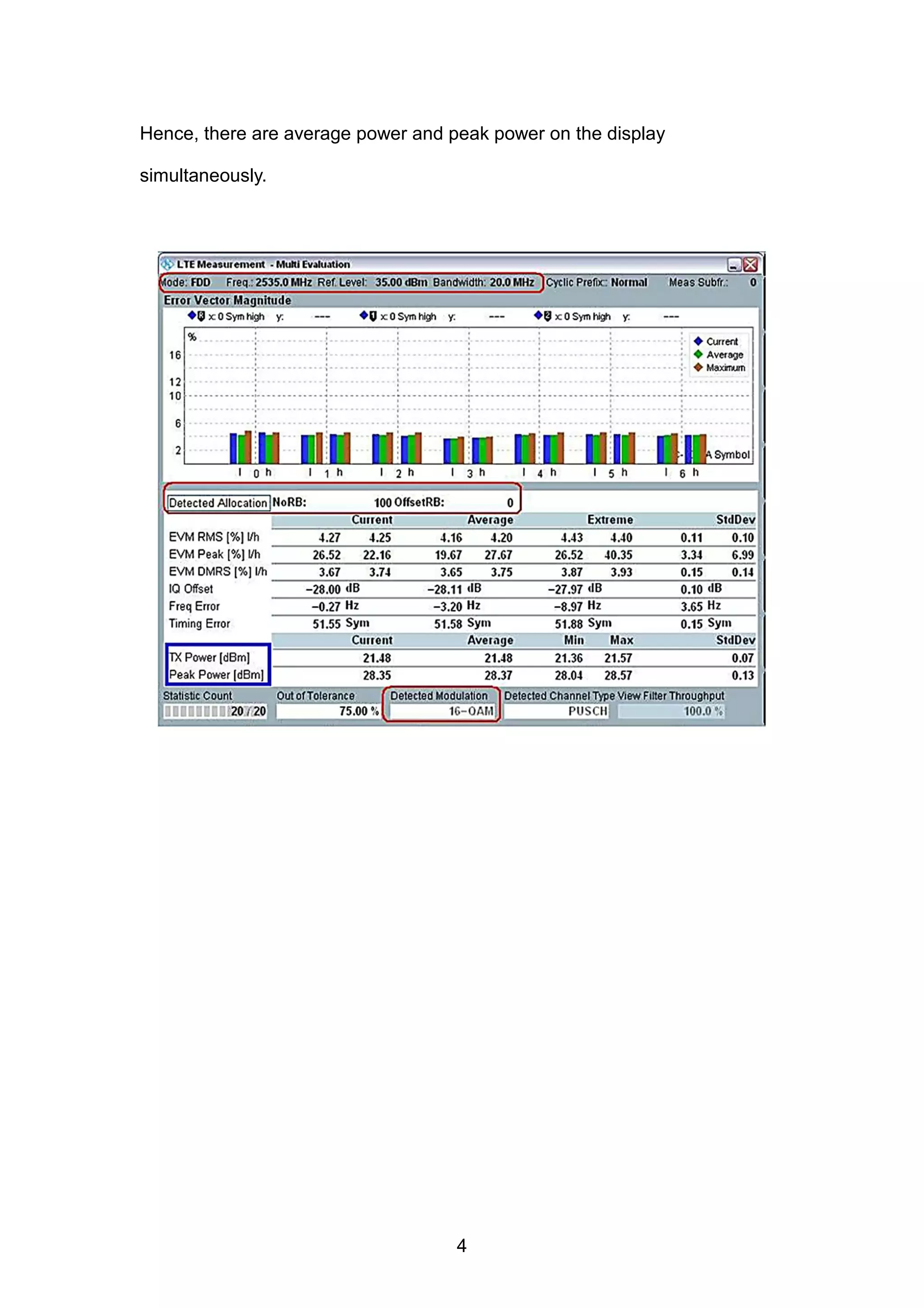
![EVM
As shown above, there are numerous test items for signal quality [6].
22](https://image.slidesharecdn.com/performancerequirementandlessonslearntoflteterminaltransmitterpart-190106204811/75/Performance-Requirement-and-Lessons-Learnt-of-LTE-Terminal_Transmitter-Part-22-2048.jpg)
![EVM (Error Vector Magnitude) is as depicted below [6]:
EVM is a vector in the I-Q plane between the ideal constellation point and the
practical point received by the receiver. In other words, it is the difference
between actual received symbols and ideal symbols. EVM is low if the actual
received symbols are very close to ideal symbols, and vice versa.
In time domain, the timing error in waveform is called “jitter”, which generates
phase error in the modulation constellation, thereby contributing to EVM [1].
23](https://image.slidesharecdn.com/performancerequirementandlessonslearntoflteterminaltransmitterpart-190106204811/75/Performance-Requirement-and-Lessons-Learnt-of-LTE-Terminal_Transmitter-Part-23-2048.jpg)
![Let’s look at the effect of LO phase noise from another point of view.
According to this relationship [12], it is apparent that the EVM is inversely
proportional to SNR. As shown below, a LO with high phase noise leads to the
reduction in RF signal SNR, thereby aggravating EVM performance.
24](https://image.slidesharecdn.com/performancerequirementandlessonslearntoflteterminaltransmitterpart-190106204811/75/Performance-Requirement-and-Lessons-Learnt-of-LTE-Terminal_Transmitter-Part-24-2048.jpg)
![As shown above, take Qualcomm WTR4905 for example, the crystal
generates a 19.2 MHz sine waveform to produce a 19.2 MHz square-wave
XO signal from PMIC to transceiver [13]. Thus, a crystal with high phase noise
contributes to the phase noise of LO. Nevertheless, cellular technology
usually shares one identical crystal with GPS technology. If GPS performance
is acceptable (i.e., CNR = 38 ~ 40 dB), it indicates that the crystal is innocent
since GPS performance is more sensitive to crystal performance thanks to its
extremely weak received signal.
25](https://image.slidesharecdn.com/performancerequirementandlessonslearntoflteterminaltransmitterpart-190106204811/75/Performance-Requirement-and-Lessons-Learnt-of-LTE-Terminal_Transmitter-Part-25-2048.jpg)
![The sine waveform and square-wave signals can corrupt each other; sufficient
isolation is highly recommended [13]. The layout shown below is a bad
example since the isolation is not enough.
Furthermore, keep-out areas on PCB top layer is necessary for transceiver
since these areas is related to VCO, which is sensitive to parasitic effect.
Otherwise, the parasitic effect may aggravate VCO phase noise [13, 30].
26](https://image.slidesharecdn.com/performancerequirementandlessonslearntoflteterminaltransmitterpart-190106204811/75/Performance-Requirement-and-Lessons-Learnt-of-LTE-Terminal_Transmitter-Part-26-2048.jpg)
![LTE makes use of OFDM (Orthogonal Frequency Division Multiplexing)
modulation [5], which is sensitive to phase error and/or frequency offset [14].
As shown below, in direct-conversion transmitter architecture, perhaps an
appreciable fraction of the PA output couples to the LO trough substrate, and
PCB traces etc. [16].
27](https://image.slidesharecdn.com/performancerequirementandlessonslearntoflteterminaltransmitterpart-190106204811/75/Performance-Requirement-and-Lessons-Learnt-of-LTE-Terminal_Transmitter-Part-27-2048.jpg)
![With the presence of injection pulling, the LO output waveform is as shown
below [16]:
As mentioned earlier, the timing error in waveform generates phase error in
the modulation constellation, thereby contributing to EVM, and OFDM
modulation is sensitive to phase error. Thus, for a LTE system, especially
direct-conversion transceiver architecture (since RF frequency almost equals
to LO frequency), oscillator pulling should be avoided.
28](https://image.slidesharecdn.com/performancerequirementandlessonslearntoflteterminaltransmitterpart-190106204811/75/Performance-Requirement-and-Lessons-Learnt-of-LTE-Terminal_Transmitter-Part-28-2048.jpg)
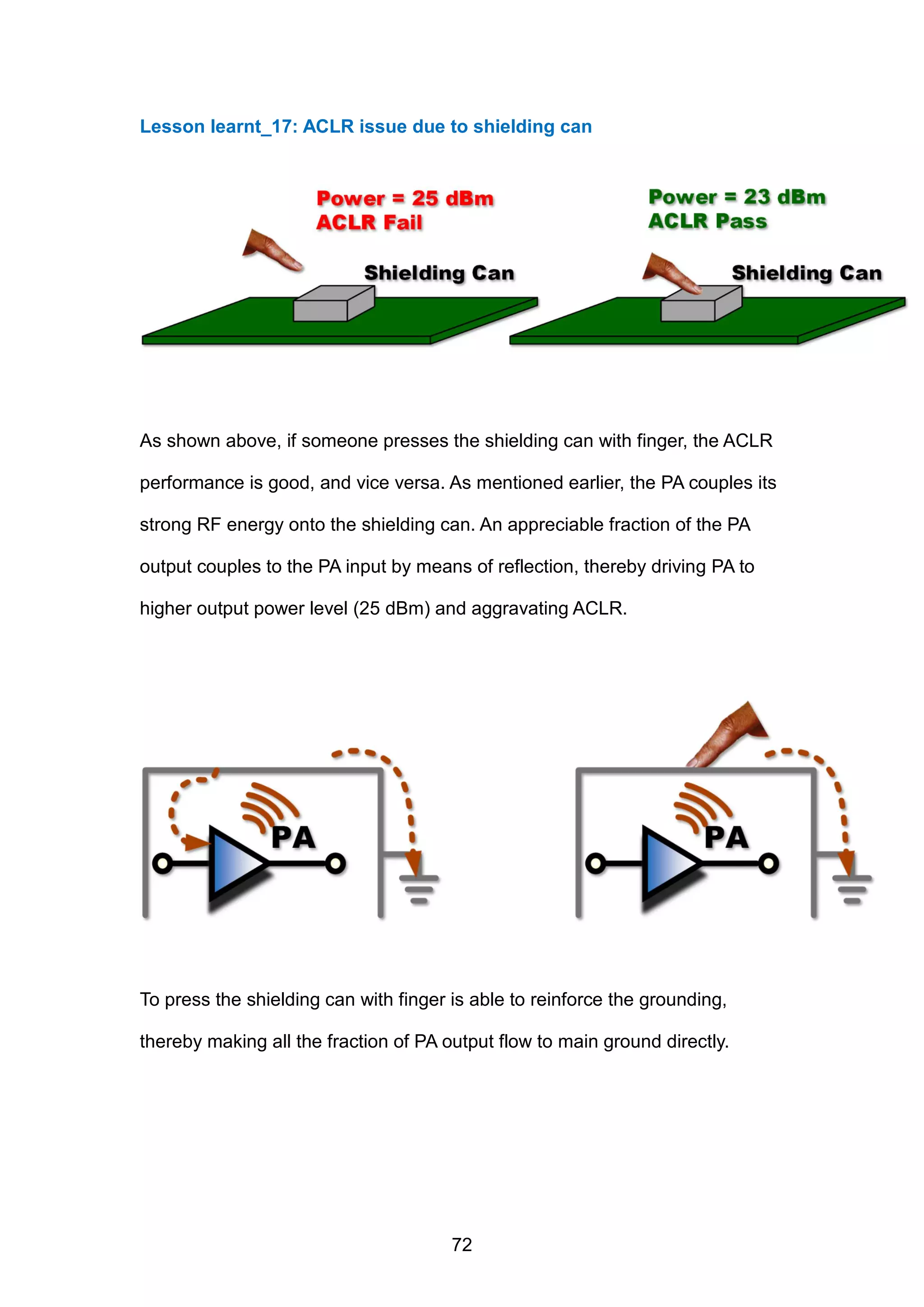
![Lesson learnt_7: EVM issue due to shielding can
As shown above, if someone presses the shielding can with finger, the EVM
performance is good, and vice versa. As shown below, PA and transceiver
blocks are placed in the identical shielding space. The PA couples its strong
RF energy onto the shielding can. An appreciable fraction of the PA output
couples to the VCO trough shielding can by means of reflection, thereby
making VCO pulling happen and aggravating EVM performance [13,18].
29](https://image.slidesharecdn.com/performancerequirementandlessonslearntoflteterminaltransmitterpart-190106204811/75/Performance-Requirement-and-Lessons-Learnt-of-LTE-Terminal_Transmitter-Part-29-2048.jpg)
![Nevertheless, if someone presses the shielding can, this action reinforces the
grounding of the shielding can, thereby eliminating reflection and VCO pulling
[13].
Thus, the PA and transceiver blocks should be placed in separated shielding
areas individually to avoid oscillator pulling [30].
Moreover, for typical designs, as the PA output exceeds 0 dBm, injection
pulling may prove severe [16].
30](https://image.slidesharecdn.com/performancerequirementandlessonslearntoflteterminaltransmitterpart-190106204811/75/Performance-Requirement-and-Lessons-Learnt-of-LTE-Terminal_Transmitter-Part-30-2048.jpg)
![As shown above, take Qualcomm SDR660 for example [19], the output power
from transceiver exceeds 0 dBm. In other words, not only PA output causes
injection pulling, but also transceiver output does. If the impedance between
transceiver and PA is NOT 50 Ohm, the reflection thanks to mismatch may
cause injection pulling [13].
31](https://image.slidesharecdn.com/performancerequirementandlessonslearntoflteterminaltransmitterpart-190106204811/75/Performance-Requirement-and-Lessons-Learnt-of-LTE-Terminal_Transmitter-Part-31-2048.jpg)
![Lesson learnt_8: B41 EVM issue due to RX path
Modern MMPAs adopt fully programmable MIPI (Mobile Industry Processor
Interface) control, which can easily enable more than one RF path
simultaneously [8,28]. B41 is TDD, receiver path should be off while
transmitter is operating. Because improper value is written into PA register,
which makes receiver path enable (marked as red circle) while transmitter is
operating. Thus, a fraction of PA output power leaks to transceiver through
receiver path, thereby causing VCO pulling. Unlike FDD system, TDD system
does NOT have duplexer to suppress TX leakage. Thus, the VCO pulling
proves severe and causes EVM issue.
32](https://image.slidesharecdn.com/performancerequirementandlessonslearntoflteterminaltransmitterpart-190106204811/75/Performance-Requirement-and-Lessons-Learnt-of-LTE-Terminal_Transmitter-Part-32-2048.jpg)
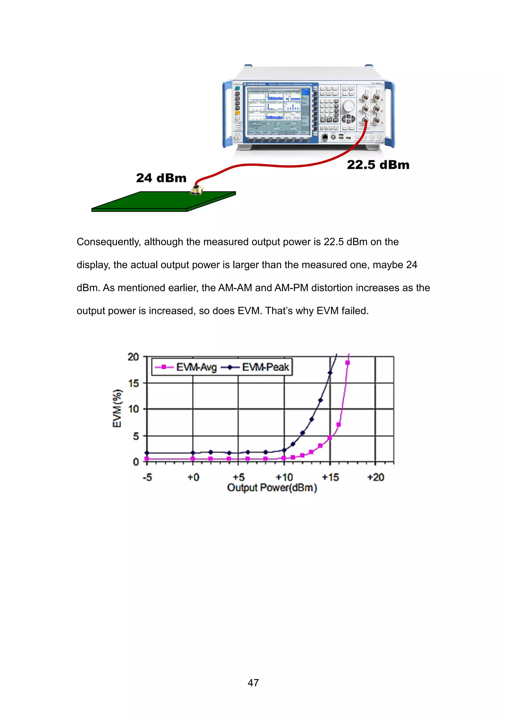
![Additionally, the PA nonlinearity, the AM-AM and AM-PM distortion, causes the
amplitude error and phase error on the output signal and then has a
contribution to EVM [1,20-21].
As shown above, the AM-AM and AM-PM distortion increases as the output
power is increased [1]. Especially, as mentioned earlier, OFDM-based
transmitter is sensitive to phase error [20]. Thus, the saturated output power
should be high enough to have more headroom, thereby causing more back-
off and better linearity [1]. This is especially important for TDD (Time Division
Duplexing) bands such as B38/B40/B41 since PA is pulsed on and off during
usage. This kind of dynamic mode has worse linearity performance than static
mode (i.e., FDD bands) [26].
33](https://image.slidesharecdn.com/performancerequirementandlessonslearntoflteterminaltransmitterpart-190106204811/75/Performance-Requirement-and-Lessons-Learnt-of-LTE-Terminal_Transmitter-Part-33-2048.jpg)
![The modulation scheme and maximum output power per band configurations
for a MMPA is as shown below [1]:
Usually, there are three ways to improve PA linearity. First, do DPD (Digital
Pre-Distortion), which is a method universally adopted and employed in
wireless cellular industry [1,5, 22].
34](https://image.slidesharecdn.com/performancerequirementandlessonslearntoflteterminaltransmitterpart-190106204811/75/Performance-Requirement-and-Lessons-Learnt-of-LTE-Terminal_Transmitter-Part-34-2048.jpg)
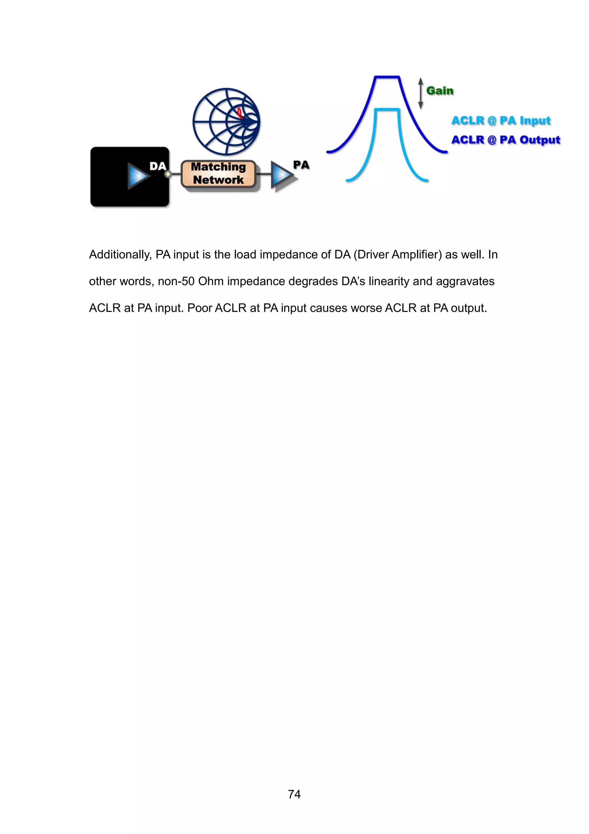
![Second, tune PA output impedance to transform the load impedance (usually
50 Ohm) into the desired one [1].
35](https://image.slidesharecdn.com/performancerequirementandlessonslearntoflteterminaltransmitterpart-190106204811/75/Performance-Requirement-and-Lessons-Learnt-of-LTE-Terminal_Transmitter-Part-35-2048.jpg)
![As shown above, the blue contour represents efficiency (%) and red contour
represents saturated power [23]. It is apparently that there is a trade-off
between efficiency and linearity. Thus, you need to optimize saturated power
at the expense of efficiency.
36](https://image.slidesharecdn.com/performancerequirementandlessonslearntoflteterminaltransmitterpart-190106204811/75/Performance-Requirement-and-Lessons-Learnt-of-LTE-Terminal_Transmitter-Part-36-2048.jpg)
![Third, tune the PA voltage supply [1]. ET (Envelope-tracking) is a technique
for improving the energy efficiency of PA. The traditional DC-DC converter
supplying (usually from PMIC directly) is replaced by a highly agile ET power
supply modulating the power supply of the PA. It means that the PA is always
operating in a highly efficient compressed state [24].
As mentioned earlier, there is a trade-off between linearity and efficiency.
Thus, ET improves efficiency at the expense of linearity. Conversely, you can
also optimize linearity at the expense of efficiency. That’s why you can tune
the PA voltage supply. Practically, you can tune ICQ (Quiescent Current) point.
37](https://image.slidesharecdn.com/performancerequirementandlessonslearntoflteterminaltransmitterpart-190106204811/75/Performance-Requirement-and-Lessons-Learnt-of-LTE-Terminal_Transmitter-Part-37-2048.jpg)
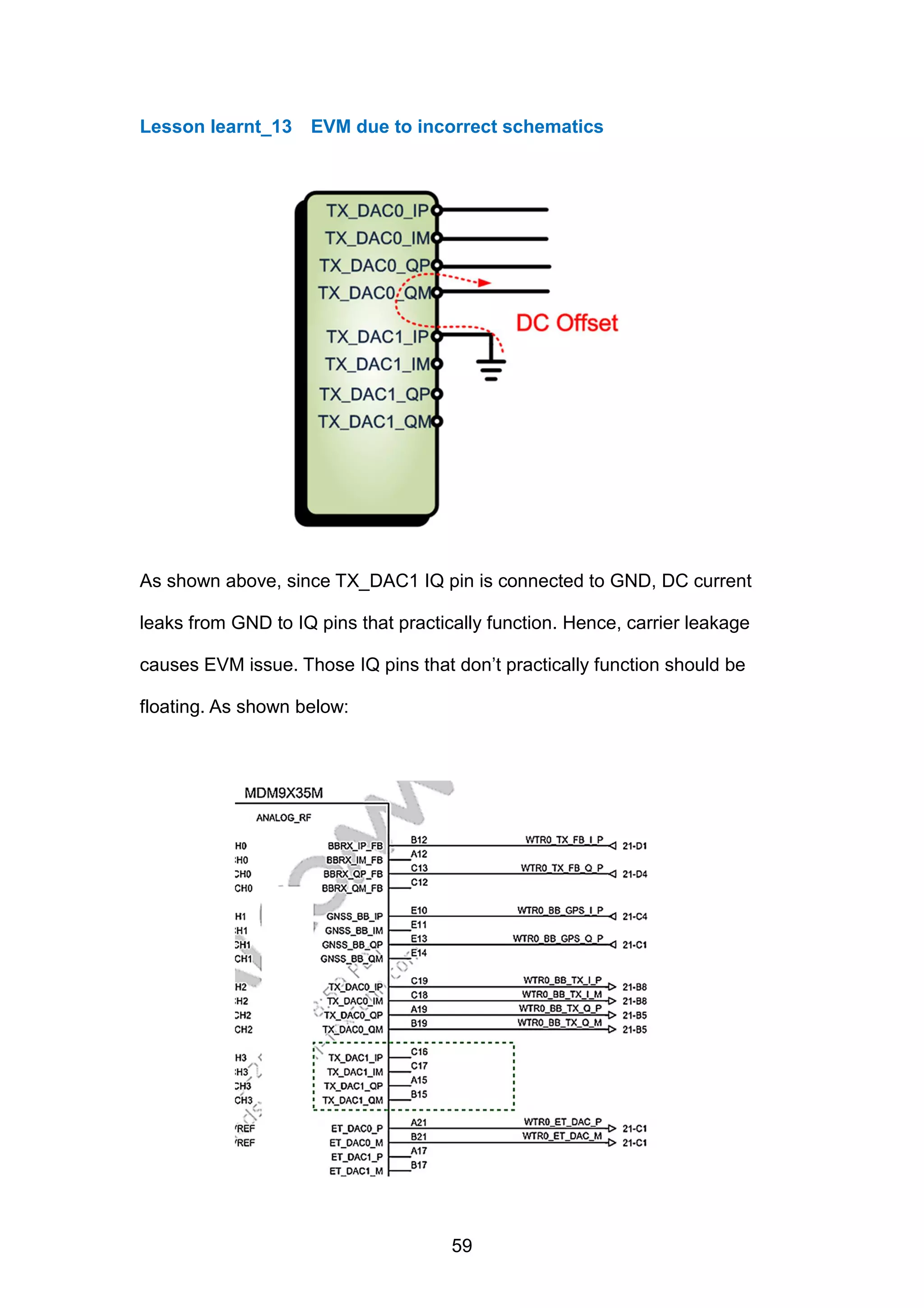
![Quadrature imperfections in the up-mixing can cause IQ imbalance, which
distorts constellation symbol location and aggravates EVM performance
[13,17,25].
Excessive DC component in I/Q branches cause high level of carrier leakage
(IQ origin offset), which also distorts constellation symbol location and
aggravates EVM performance [13].
38](https://image.slidesharecdn.com/performancerequirementandlessonslearntoflteterminaltransmitterpart-190106204811/75/Performance-Requirement-and-Lessons-Learnt-of-LTE-Terminal_Transmitter-Part-38-2048.jpg)
![As shown above, “1” is just RF transmitting signal, “2” is carrier leakage, and
“3” is called “image” thanks to IQ imbalance [6].
39](https://image.slidesharecdn.com/performancerequirementandlessonslearntoflteterminaltransmitterpart-190106204811/75/Performance-Requirement-and-Lessons-Learnt-of-LTE-Terminal_Transmitter-Part-39-2048.jpg)
![Consequently, calibration is necessary for improving IQ imbalance and carrier
leakage [13].
40](https://image.slidesharecdn.com/performancerequirementandlessonslearntoflteterminaltransmitterpart-190106204811/75/Performance-Requirement-and-Lessons-Learnt-of-LTE-Terminal_Transmitter-Part-40-2048.jpg)
![As mentioned earlier, the XO signal from PMIC to transceiver is rich in
harmonics (i.e., 19.2 MHz*N, N is integer). Thus, IQ traces should be away
from XO signal. Otherwise, those channels, whose frequencies correspond to
19.2 MHz*N, may have EVM issue. Please reserve LC filter in IQ traces, as
shown below [13]:
41](https://image.slidesharecdn.com/performancerequirementandlessonslearntoflteterminaltransmitterpart-190106204811/75/Performance-Requirement-and-Lessons-Learnt-of-LTE-Terminal_Transmitter-Part-41-2048.jpg)
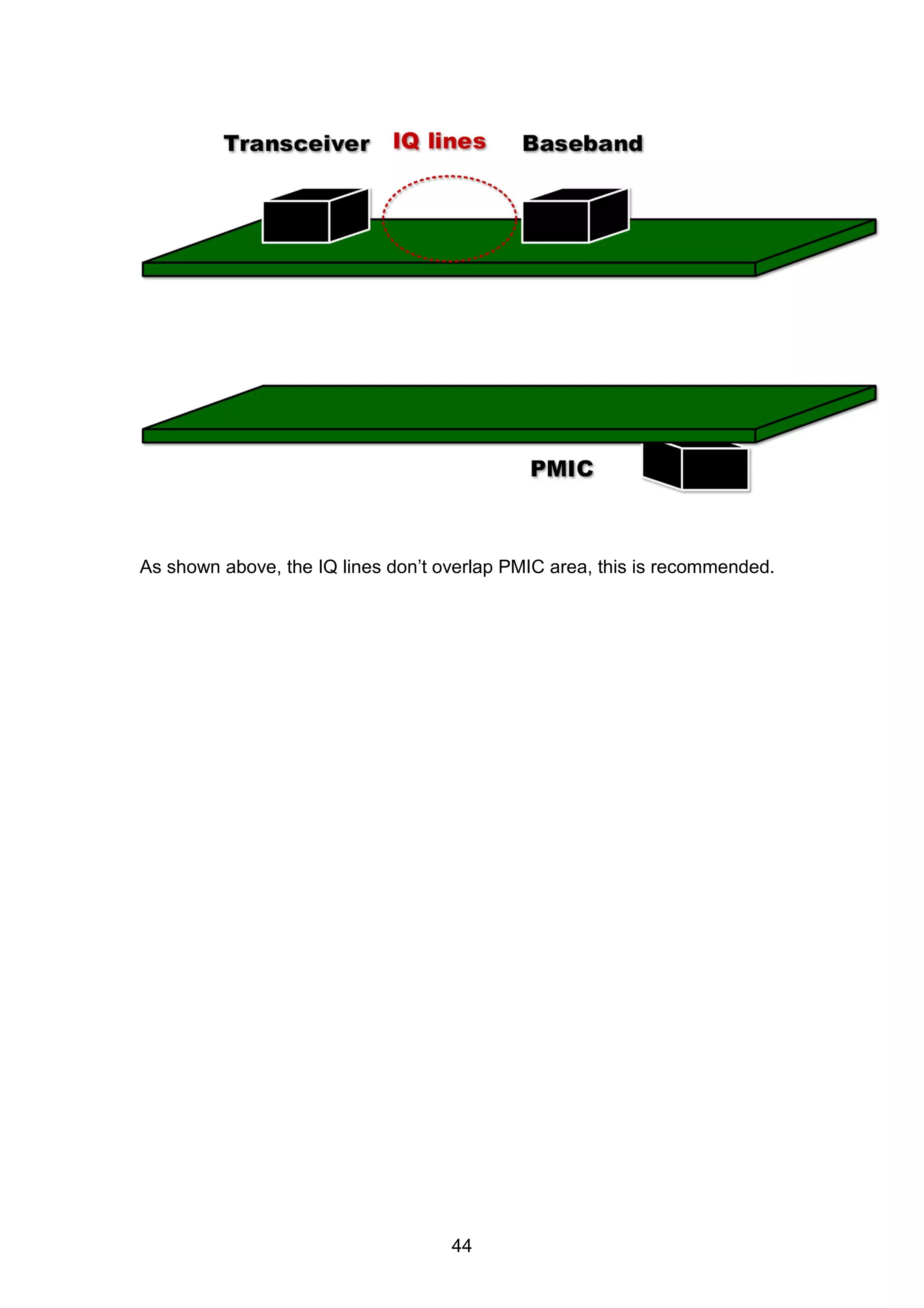
![Besides, avoid routing IQ lines near or directly under PMIC SMPS (Switching
Mode Power Supply) PCB areas since the strong switching noise can couple
magnetically and electrically to IQ lines even though in the presence of GND
plane separation. As shown below, the case where the IQ traces are
separated from PMIC switching node by multiple ground layers, but it is not
recommended [30].
43](https://image.slidesharecdn.com/performancerequirementandlessonslearntoflteterminaltransmitterpart-190106204811/75/Performance-Requirement-and-Lessons-Learnt-of-LTE-Terminal_Transmitter-Part-43-2048.jpg)
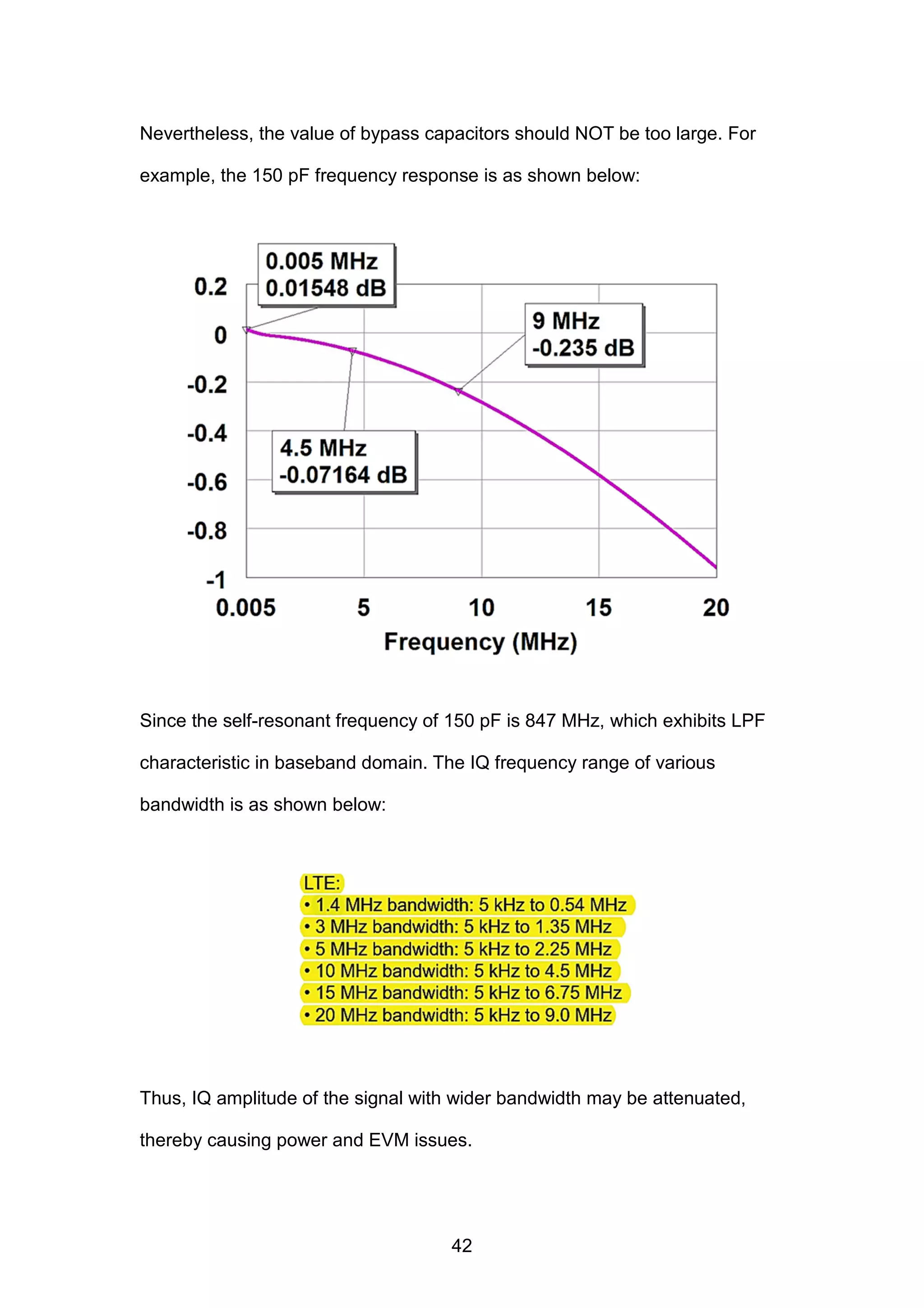
![Filter contributes to EVM as well. As mentioned earlier, DPD is a method to
improve linearity. Nevertheless, during DPD, the pre-distorted waveform will
be truncated if the filter bandwidth is not wide enough, thereby contributing to
EVM [5].
Besides, the deviations in group delay cause signal distortion [5].
48](https://image.slidesharecdn.com/performancerequirementandlessonslearntoflteterminaltransmitterpart-190106204811/75/Performance-Requirement-and-Lessons-Learnt-of-LTE-Terminal_Transmitter-Part-48-2048.jpg)
![Usually, large group delay variation appears near the transition region in
frequency response, leading to distorted waveform [5].
Thus, with large deviations in group delay, the channels near the transition
region suffer from EVM issue more easily. The total EVM of an LTE signal is
as calculated below [5]:
EVMi is the EVM measured across the individual RB. N is the total number of
RBs in the LTE signal. EVMi can be as calculated below:
∆α is the effective magnitude ripple across the individual RB of the filter’s
passband; ∆ø is the effective phase ripple across the individual RB of the
filter’s passband [5].
49](https://image.slidesharecdn.com/performancerequirementandlessonslearntoflteterminaltransmitterpart-190106204811/75/Performance-Requirement-and-Lessons-Learnt-of-LTE-Terminal_Transmitter-Part-49-2048.jpg)
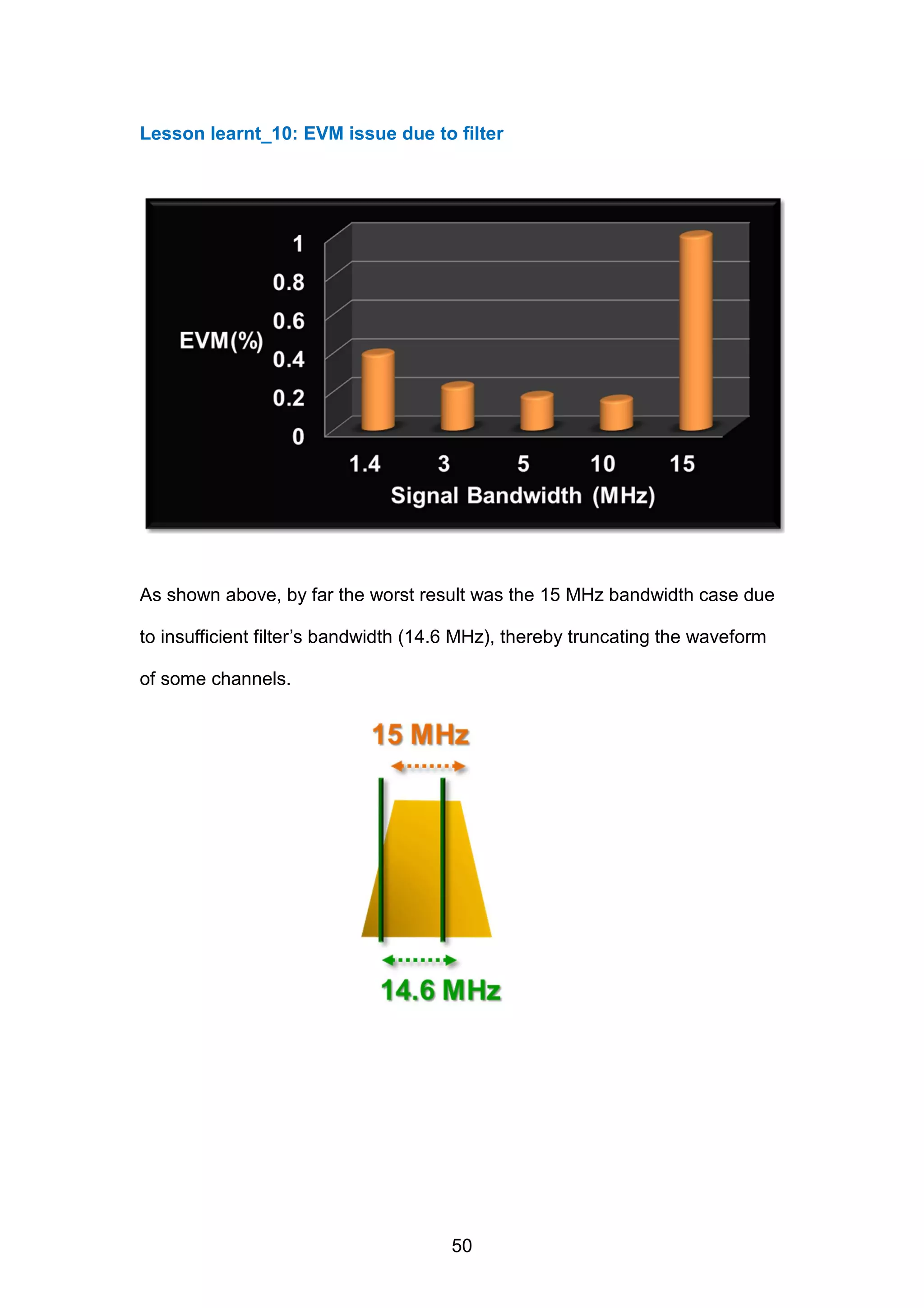
![Furthermore, except 15 MHz, it is apparently that narrower bandwidth results
in worse EVM. It is related to proportion. For instance, with 1.4 MHz signal
bandwidth, if three RBs are contaminated by large group delay ripple near
transition region (e.g. low/high channel), it means that 50% RBs (3/6 = 50%)
have poor EVM, thereby aggravating the overall EVM.
Conversely, with 10 MHz signal bandwidth, even though 5 RBs are
contaminated by large group delay ripple near transition region, it means that
merely 10% RBs (5/50 = 10%) have poor EVM, which is not severe enough to
the overall EVM [5].
Thus, what matters most is that how much the proportion is, not how much
the contaminated RB number is.
51](https://image.slidesharecdn.com/performancerequirementandlessonslearntoflteterminaltransmitterpart-190106204811/75/Performance-Requirement-and-Lessons-Learnt-of-LTE-Terminal_Transmitter-Part-51-2048.jpg)
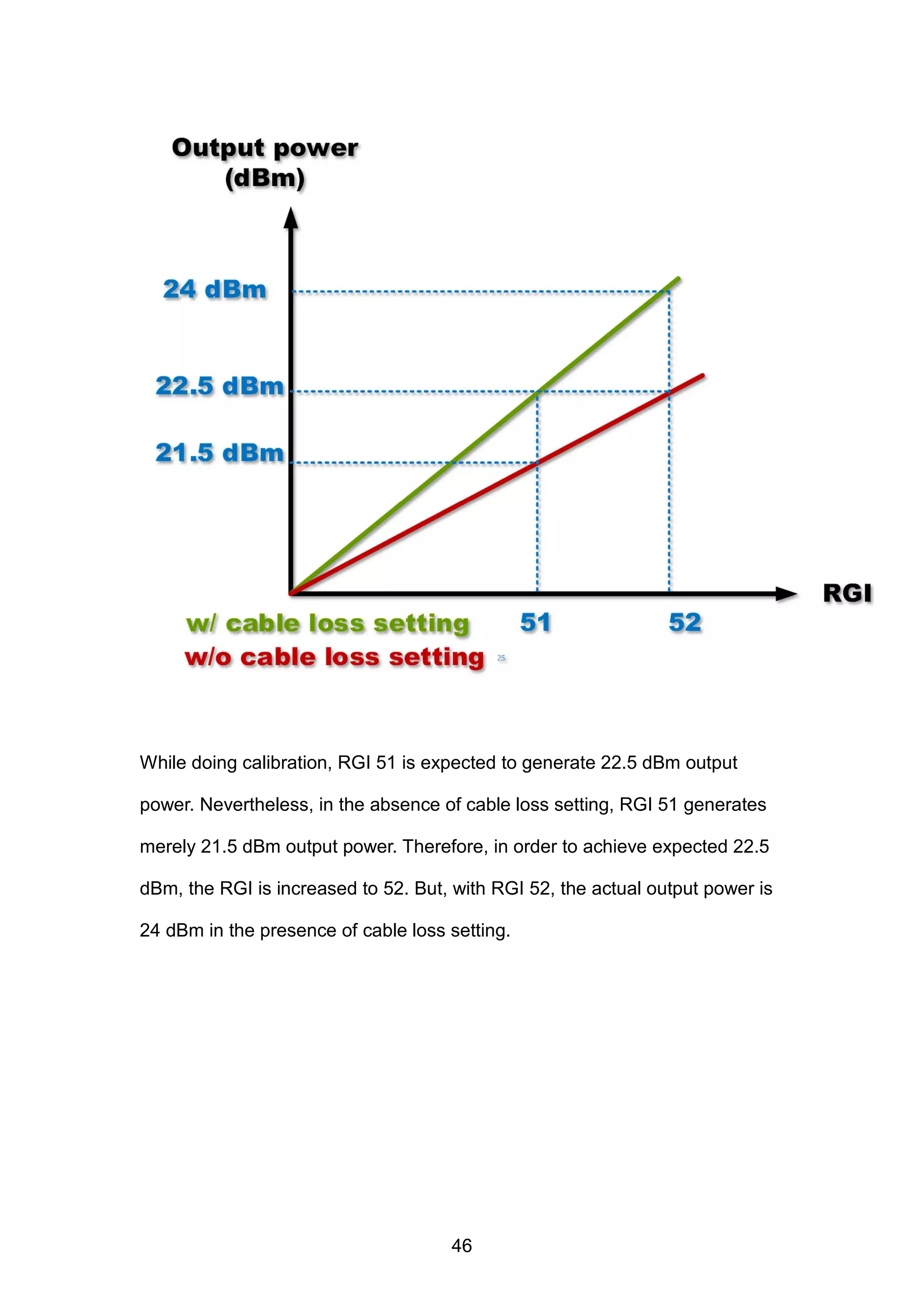
![In addition to group delay ripple and bandwidth, temperature stability is a
crucial factor contributing to EVM as well. As shown below, the frequency
response may drift towards the left side in high temperature.
Thus, during calibration, perhaps the growing heat in PCB makes the
frequency response drift towards the left side, thereby reinforcing the loss in
high channel and the output power is not as expected. At this time, as
mentioned earlier, the RGI is increased to compensate for the loss so as to
achieve expected power. This causes too high output power in high channel
under normal temperature, thereby aggravating EVM [5].
52](https://image.slidesharecdn.com/performancerequirementandlessonslearntoflteterminaltransmitterpart-190106204811/75/Performance-Requirement-and-Lessons-Learnt-of-LTE-Terminal_Transmitter-Part-52-2048.jpg)
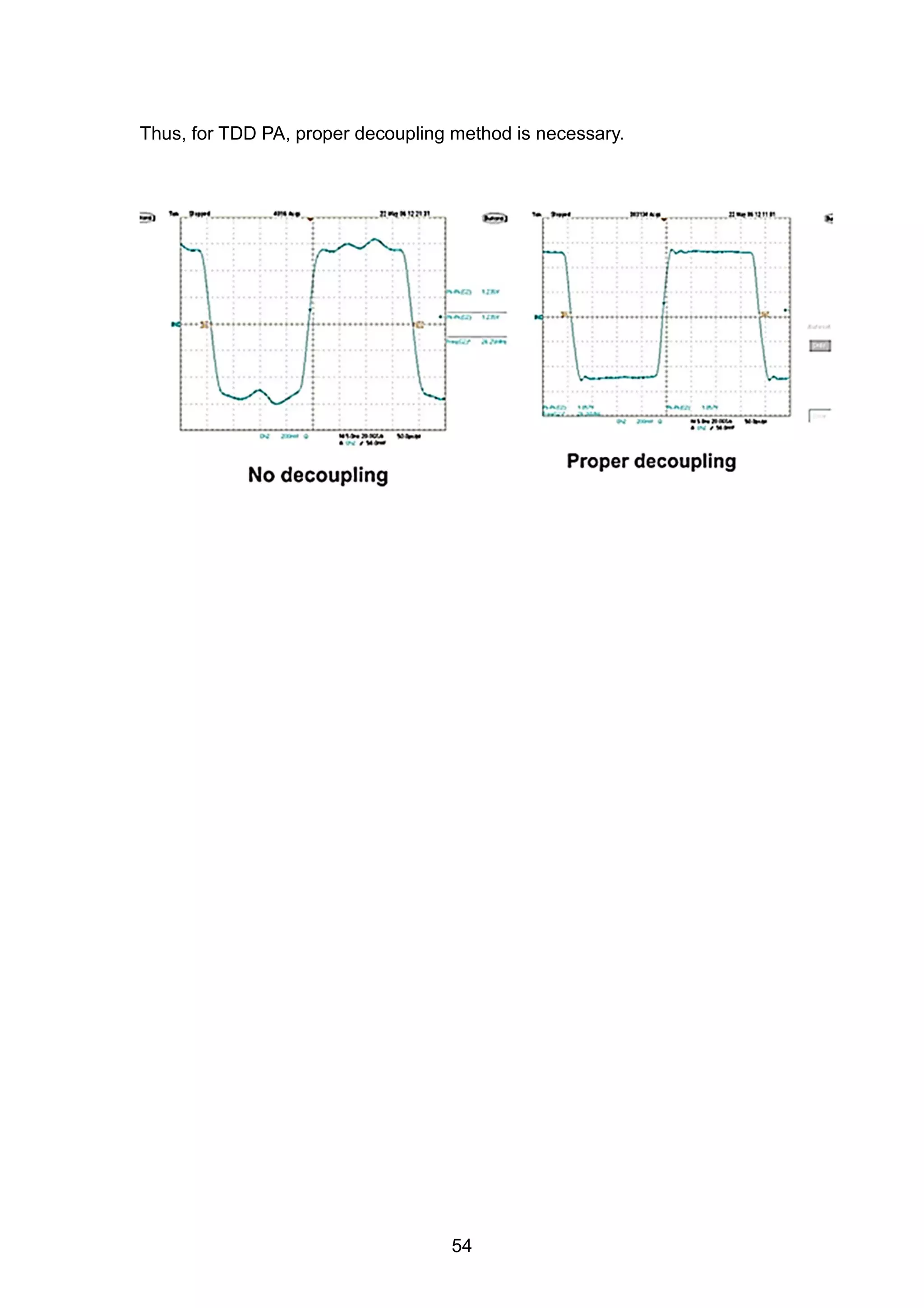
![As mentioned earlier, TDD bands have worse linearity performance than FDD
bands. Additionally, for TDD PA, once PA is on, amplitude must be flat during
entire transmission. Otherwise, any rise or droop contributes to AM/AM
distortion and degrades EVM [26]. So TX related timing (PA_ON, ASM, etc.) is
crucial [31].
Furthermore, thanks to dynamic mode operation, once PA in on, the power
supply generates huge transient current, thereby aggravating voltage ripple
[13].
Any imperfection in power supply (e.g. IR drop, ripple, noise) causes poor
transmitter performance.
53](https://image.slidesharecdn.com/performancerequirementandlessonslearntoflteterminaltransmitterpart-190106204811/75/Performance-Requirement-and-Lessons-Learnt-of-LTE-Terminal_Transmitter-Part-53-2048.jpg)
![As for transceiver, pay attention to not only keep-out areas, but also power
supply. Use star-routing for power supply pins rather than daisy-chain [30].
55](https://image.slidesharecdn.com/performancerequirementandlessonslearntoflteterminaltransmitterpart-190106204811/75/Performance-Requirement-and-Lessons-Learnt-of-LTE-Terminal_Transmitter-Part-55-2048.jpg)
![As shown above, there are five power supply sources from PMIC to
transceiver, four of them (as marked green circle) provide to multiple pins. It is
necessary to make use of star-routing for these pins. Branch at capacitor (as
marked black circle) only [30].
56](https://image.slidesharecdn.com/performancerequirementandlessonslearntoflteterminaltransmitterpart-190106204811/75/Performance-Requirement-and-Lessons-Learnt-of-LTE-Terminal_Transmitter-Part-56-2048.jpg)
![Lesson learnt_11 EVM issue due to LCM
As shown above, EVM fails while LCM is on, but passes while LCM is off. As
shown below, since VPH_PWR branches close to backlight driver IC, thereby
causing the impedance of the coupling path low. Thus, transient current from
backlight driver IC leaks to MMPA easily. That’s why EVM passes while LCM
off due to the absence of transient current [13].
57](https://image.slidesharecdn.com/performancerequirementandlessonslearntoflteterminaltransmitterpart-190106204811/75/Performance-Requirement-and-Lessons-Learnt-of-LTE-Terminal_Transmitter-Part-57-2048.jpg)
![Lesson learnt_12 EVM issue due to WIFI
As shown above, EVM fails while LTE and WIFI operate simultaneously. As
shown below, there is no sufficient isolation between cellular and WIFI XO
traces. As mentioned earlier, XO signal is rich in harmonics, so they interfere
with each other in this case [35].
58](https://image.slidesharecdn.com/performancerequirementandlessonslearntoflteterminaltransmitterpart-190106204811/75/Performance-Requirement-and-Lessons-Learnt-of-LTE-Terminal_Transmitter-Part-58-2048.jpg)
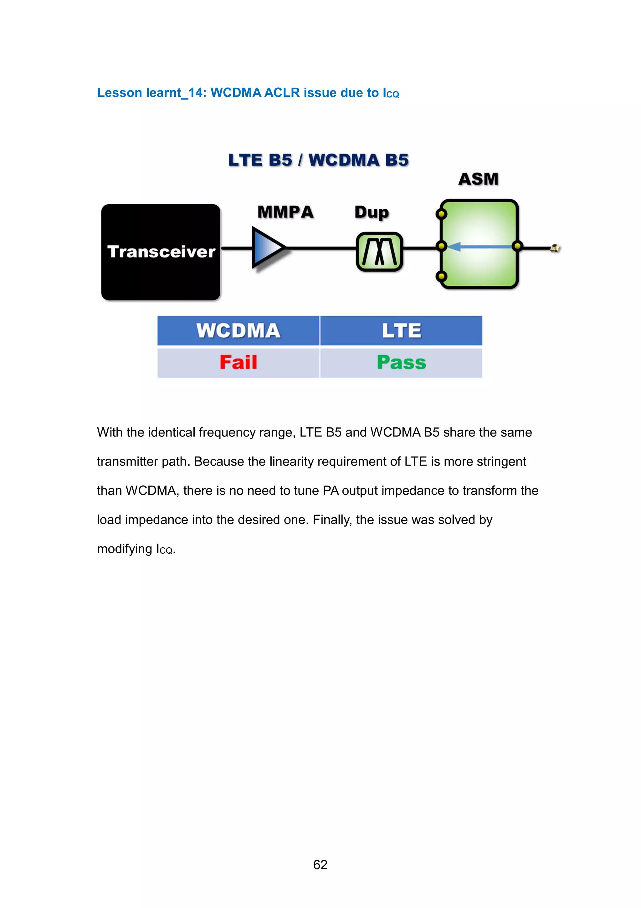
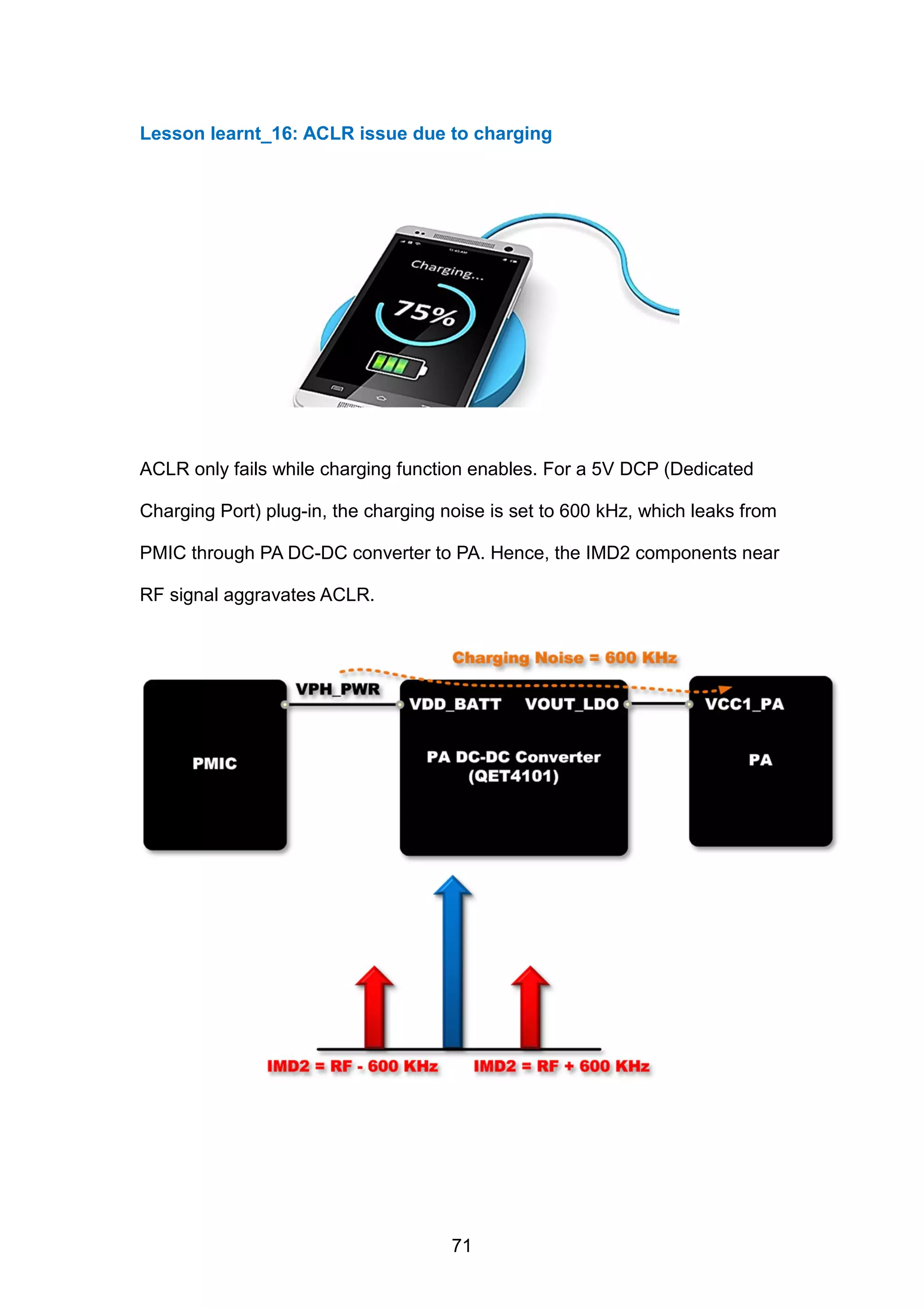
![ACLR
As shown above, the IMD (Intermodulation) contributes to ACLR. Therefore,
the linearity of transmitter chain, especially PA, determines the ACLR
performance [6,27].
60](https://image.slidesharecdn.com/performancerequirementandlessonslearntoflteterminaltransmitterpart-190106204811/75/Performance-Requirement-and-Lessons-Learnt-of-LTE-Terminal_Transmitter-Part-60-2048.jpg)
![As mentioned earlier, SC-FDMA is used for LTE uplink transmission to reduce
PAR [1,5]. Nevertheless, LTE still has higher PAR in uplink modulation than
WCDMA. Thus, even though in the presence of smaller output power (LTE:23
dBm, WCDMA:24 dBm), LTE still has worse ACLR performance due to higher
PAR. In other words, the linearity requirement of LTE is more stringent than
WCDMA.
61](https://image.slidesharecdn.com/performancerequirementandlessonslearntoflteterminaltransmitterpart-190106204811/75/Performance-Requirement-and-Lessons-Learnt-of-LTE-Terminal_Transmitter-Part-61-2048.jpg)
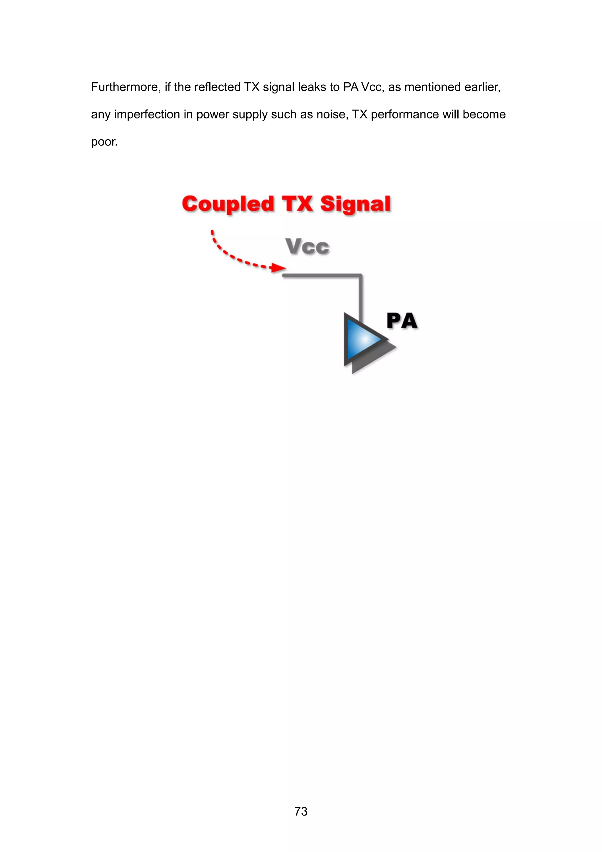
![For ET, it is crucial that Vcc and the RF input signal are aligned in time of the
PA. Otherwise, these will be time delay between RF input signal and Vcc,
thereby aggravating transmitter performance, such as ACLR and EVM [29].
Thus, proper time delay adjustment is necessary.
63](https://image.slidesharecdn.com/performancerequirementandlessonslearntoflteterminaltransmitterpart-190106204811/75/Performance-Requirement-and-Lessons-Learnt-of-LTE-Terminal_Transmitter-Part-63-2048.jpg)
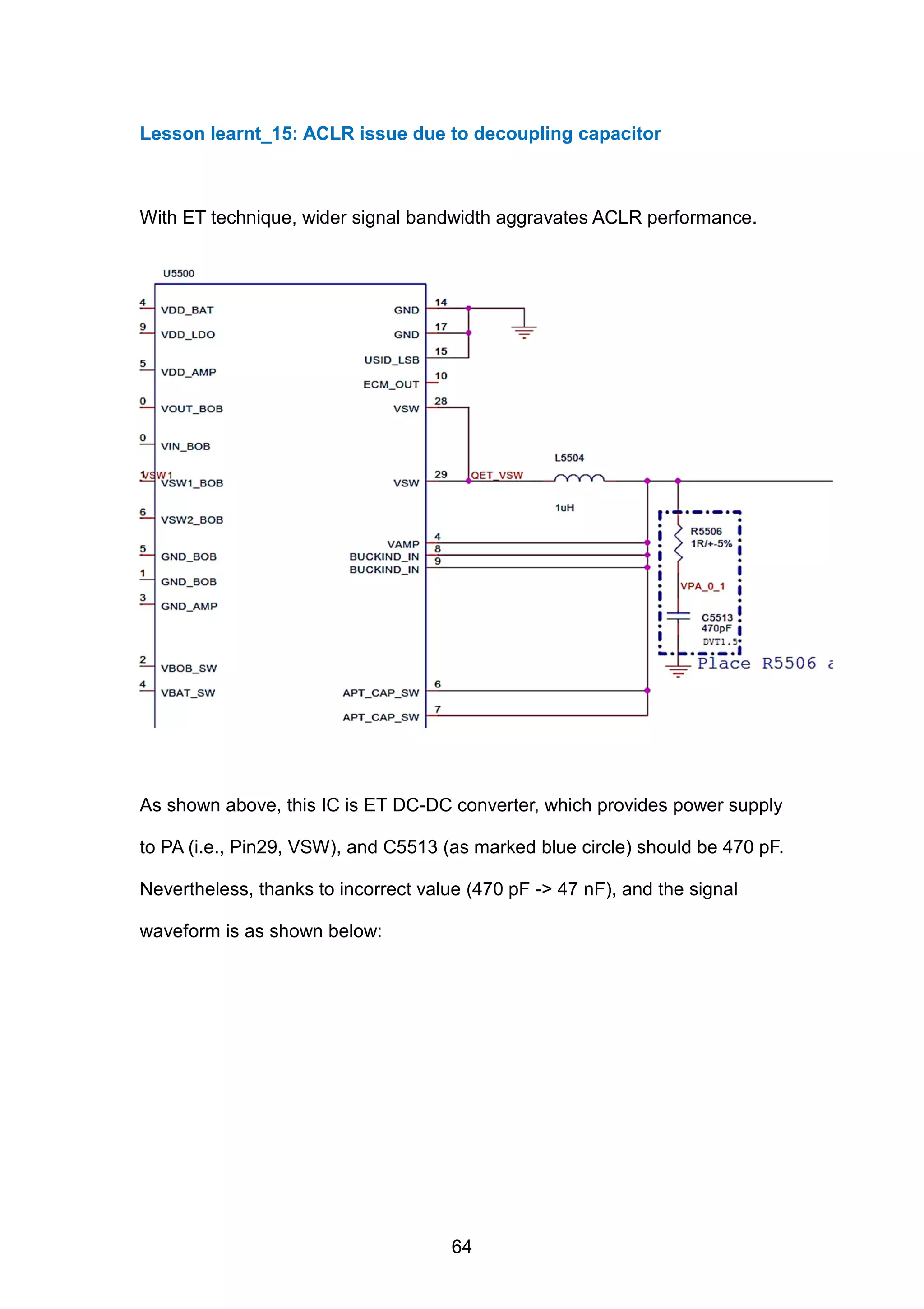
![In 20 MHz bandwidth, the time delay between Vcc (yellow trace) and RF input
signal is obvious thanks to 47 nF shunt capacitor, thereby causing ACLR
issue. As shown below, N is the number of subcarriers, which is related to
PAR and bandwidth. In other words, wider bandwidth has higher PAR [5].
High PAR means that the envelope varies more quickly than low PAR, so the
time delay of 20 MHz bandwidth is more serious than 5 MHz one. Of course,
with an external power supply (i.e., conventional fixed power supply) rather
than ET DC-DC converter, the issue is gone.
65](https://image.slidesharecdn.com/performancerequirementandlessonslearntoflteterminaltransmitterpart-190106204811/75/Performance-Requirement-and-Lessons-Learnt-of-LTE-Terminal_Transmitter-Part-65-2048.jpg)
![Occasionally, the ACLR is asymmetric, which is related to memory effects in
PA. Memory effects are changes in a PA’s nonlinearity resulting from the
previous history of the input signal [32]. Self-heating has already been proven
to be one of the key sources to memory effect in PA. In addition, the memory
effect depends on signal bandwidth as well [33]. Therefore, asymmetric ACLR
phenomena often occurs in maximum output power, especially wider
bandwidth. The solution to this issue is to tune PA load impedance [34].
66](https://image.slidesharecdn.com/performancerequirementandlessonslearntoflteterminaltransmitterpart-190106204811/75/Performance-Requirement-and-Lessons-Learnt-of-LTE-Terminal_Transmitter-Part-66-2048.jpg)
![Tune the impedance from antenna port to duplexer first to shrink the circle,
then tune the impedance from PA and duplexer to determine the circle
location in Smith Chart. Nevertheless, in this case, for connector signal pad,
to regard L9 as GND proves severe mismatch due to merely 14 Ohm [13].
68](https://image.slidesharecdn.com/performancerequirementandlessonslearntoflteterminaltransmitterpart-190106204811/75/Performance-Requirement-and-Lessons-Learnt-of-LTE-Terminal_Transmitter-Part-68-2048.jpg)
![Therefore, in this case, it is very difficult to pull load impedance to 50 Ohm for
the common path [13]. Thus, for PA, ASM. and connector etc., metal under
their signal pads should be cut out to retain 50 Ohm, if necessary. In this
case, L9, L8, and L7 should be cut out to retain 50 Ohm (GND is L6).
69](https://image.slidesharecdn.com/performancerequirementandlessonslearntoflteterminaltransmitterpart-190106204811/75/Performance-Requirement-and-Lessons-Learnt-of-LTE-Terminal_Transmitter-Part-69-2048.jpg)
![Ideally, the baseband signal is mixed with an up-converter (LO) to obtain the
(LO + BB) component at transceiver output. Nevertheless, practically, the LO
often generates square-wave signal which is rich in harmonics. Thus, there
will be (LO ± BB) and (3LO ± BB) at mixer output.
Thus, if not properly filtered before PA, (LO ± BB) components due to PA
nonlinearity appears near RF signal, thereby aggravating ACLR [31].
70](https://image.slidesharecdn.com/performancerequirementandlessonslearntoflteterminaltransmitterpart-190106204811/75/Performance-Requirement-and-Lessons-Learnt-of-LTE-Terminal_Transmitter-Part-70-2048.jpg)
![Reference
[1] LTE for UMTS Evolution to LTE-Advanced second edition
[2] IIP2 Requirements in 4G LTE Handset Receivers
[3] Comparison of 8-QAM, 16-QAM, 32-QAM, 64-QAM 128-QAM, 256-QAM,
etc
[4] Next-Generation Variable-Line-Rate Optical WDM Networks: Issues and
Challenges
[5] EVM Degradation in LTE Systems by RF Filtering
[6] LTE measurements – from RF to application testing, R&S
[7] Conducting Measurements on LTE Transmitters
[8] SKY77645-11 SkyLiTE™ Multimode Multiband Power Amplifier Module,
SKYWORKS
[9] SKY77912-11 Tx-Rx FEM for Quad-Band GSM / GPRS / EDGE w/ 10
Linear TRx Switch Ports, Dual-Band TD-SCDMA, and TDD LTE Band 39,
SKYWORKS
[10] Min power issue based on RF54** design, Qualcomm
[11] CDMA Zero-IF Receiver Consideration
[12] A Method to Assess Analog Front-End Performance in Communication
SoCs, Synopsys
[13] Analysis of GSM ORFS issue
[14] BER Sensitivity of OFDM Systems to Carrier Frequency Offset and
Wiener
Phase Noise, IEEE
[15] A study of injection locking and pulling in oscillators, IEEE
75](https://image.slidesharecdn.com/performancerequirementandlessonslearntoflteterminaltransmitterpart-190106204811/75/Performance-Requirement-and-Lessons-Learnt-of-LTE-Terminal_Transmitter-Part-75-2048.jpg)
![[16] RF Microelectronics 2nd edition, Razavi
[17] Introduction to Modern Receiver
[18] Pulling Mitigation in Wireless Transmitters, IEEE
[19] SDR660 Wafer-level RF Transceiver Device Specification, Qualcomm
[20] Analysis and Compensation of the AM-AM and AM-PM Distortion for
CMOS Cascade Class-E Power Amplifier
[21] Linear GaN MMIC combined power amplifiers for 7-GHz microwave
backhaul
[22] Ultrawideband Digital Predistortion (DPD): The Rewards (Power and
Performance) and Challenges of Implementation in Cable Distribution
Systems,
[23] QFE2340 V3.X APT + DPD Matching Guidelines and Loadpull Contours,
Qualcomm
[24] Modelling envelope-tracking RF PAs for LTE at high dynamic range
[25] Introduction to IQ signal
[26] CHALLENGES IN DESIGNING 5 GHZ 802.11AC WIFI POWER
AMPLIFIERS
[27] CMOS linear high performance push amplifier for WiMAX power amplifier
[28] Introduction to Antenna impedance Tuner and Aperture Switch
[29] Envelope Tracking and Digital Pre-Distortion Test Solution for
Amplifiers application note, R&S
[30] WTR4905/WTR4605 RF Transceiver training slides, Qualcomm
[31] LTE Technology Troubleshooting Guidelines, Qualcomm
[32] MINIMIZING POWER AMPLIFIER MEMORY EFFECTS
[33] Self-heating and Memory Effects in RF Power Amplifiers Explained
Through Electro-Thermal Modeling
76](https://image.slidesharecdn.com/performancerequirementandlessonslearntoflteterminaltransmitterpart-190106204811/75/Performance-Requirement-and-Lessons-Learnt-of-LTE-Terminal_Transmitter-Part-76-2048.jpg)
![[34] MSM8974/MDM9x25 RF Customer Issues, Qualcomm
[35] MSM8926/MSM8x26/ MSM8x10 RF Common Issues, Qualcomm
77](https://image.slidesharecdn.com/performancerequirementandlessonslearntoflteterminaltransmitterpart-190106204811/75/Performance-Requirement-and-Lessons-Learnt-of-LTE-Terminal_Transmitter-Part-77-2048.jpg)

1. The document discusses transmitter output power specifications for LTE and WCDMA, including maximum output power levels and tolerances. 2. It provides lessons learned from issues with output power, EVM, and other signal quality metrics on various device bands. Common causes included improper gain mode selection, impedance mismatches, and oscillator pulling from strong RF signals. 3. Key recommendations include separating PA and transceiver shielding areas, compensating output power for temperature and frequency variations, avoiding routing near noise sources, and using proper gain/loss configurations.
Discusses maximum output power for LTE (23 dBm) and WCDMA (24 dBm) with tolerances.
Compares modulation types used in LTE (QPSK, 16QAM, 64QAM) and WCDMA (BPSK).
Higher order modulation increases data rate but raises Peak-to-Average Ratio, requiring power management.
Discusses SC-FDMA for LTE, maximum power reduction and influences of temperature on output power.
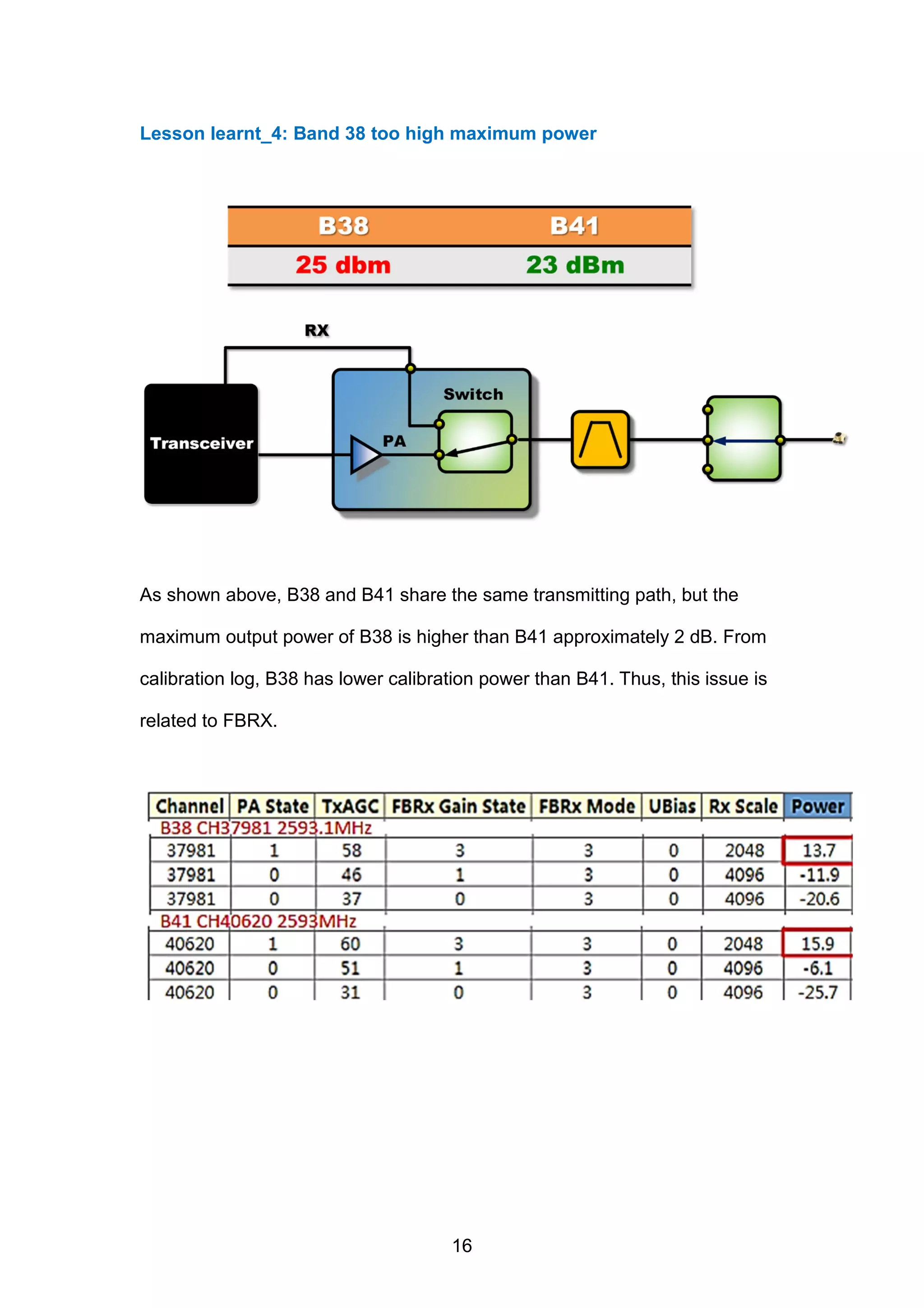
Differentiates performance in low and high gain modes; highlights calibration issues between bands B27 and B28.
Investigates maximum power behavior in Band 2 and its channels, along with feedback path responses.
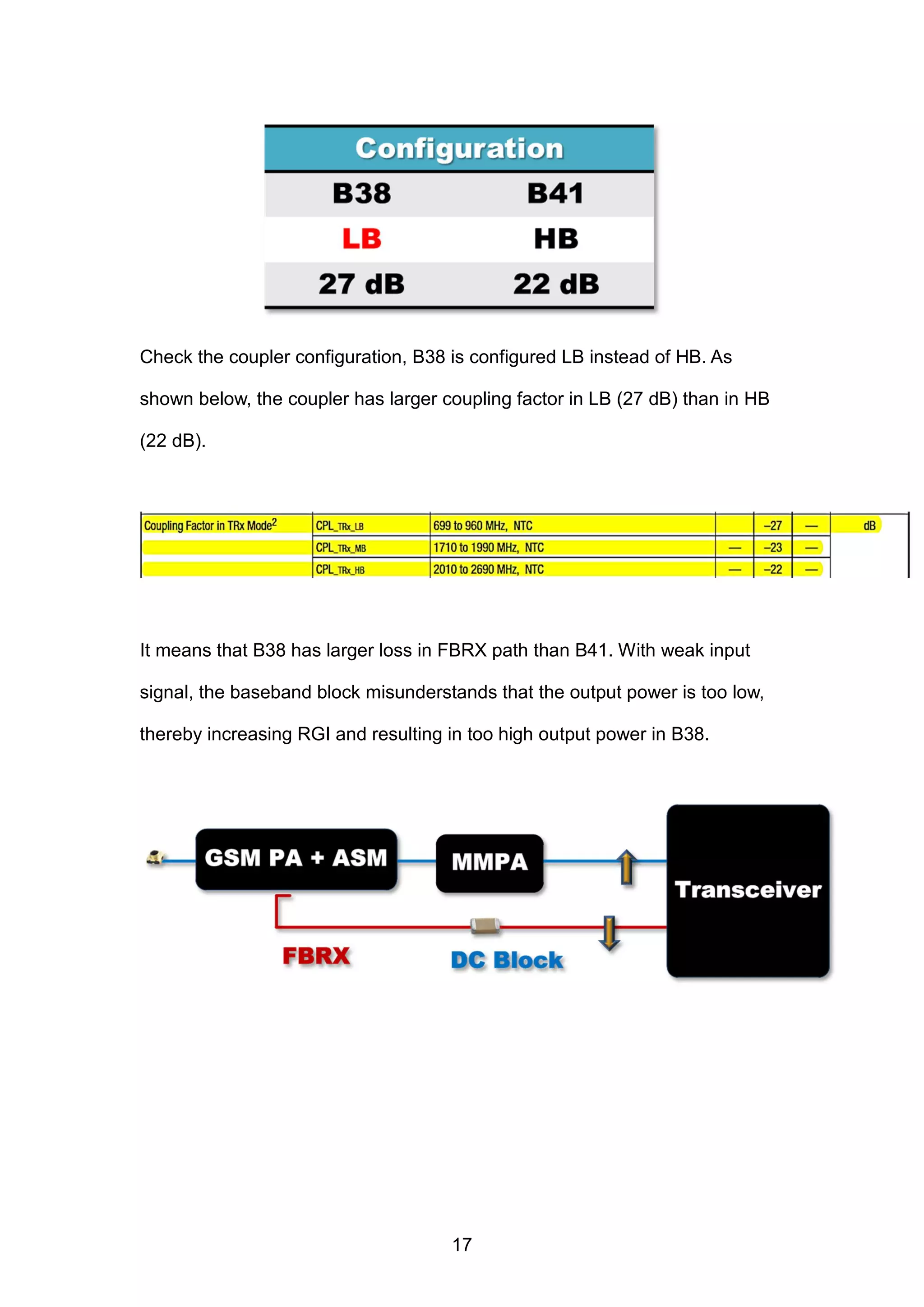
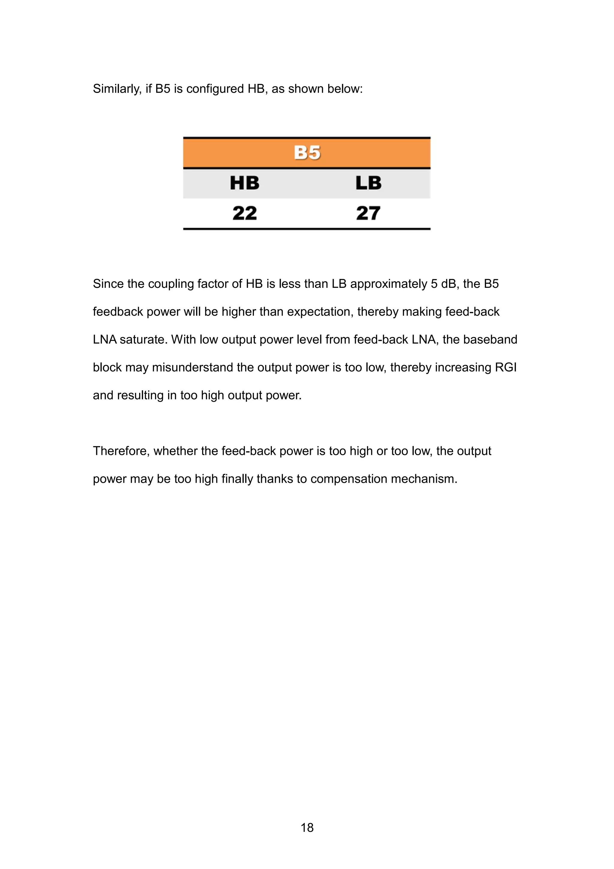
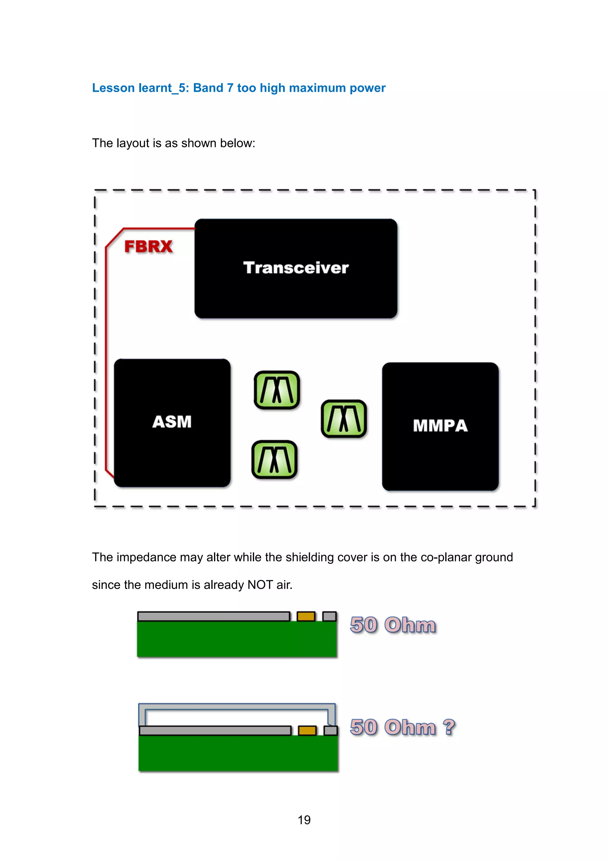
Various lessons learned addressing excessive output power issues due to faulty configurations and feedback channels.
Explains EVM calculation, effects from phase noise in LO, and issues related to shielding and geometry.
Describes risks of component interference and compensations ensuring linearity and minimizing distortion.
Three methods for enhancing PA linearity: DPD, impedance tuning, and voltage supply tuning outlined.
Focuses on calibration necessities for correcting IQ imbalance and related interference issues.
Discusses factors like group delay, temperature stability, and filter bandwidth impacting EVM results.
Explains challenges in PA timing and supply imperfections significantly affecting TDD performance.
Series of lessons learned detailing interference issues from various components affecting EVM and ACLR.
Lists references and sources used for compiling the presentation content.