
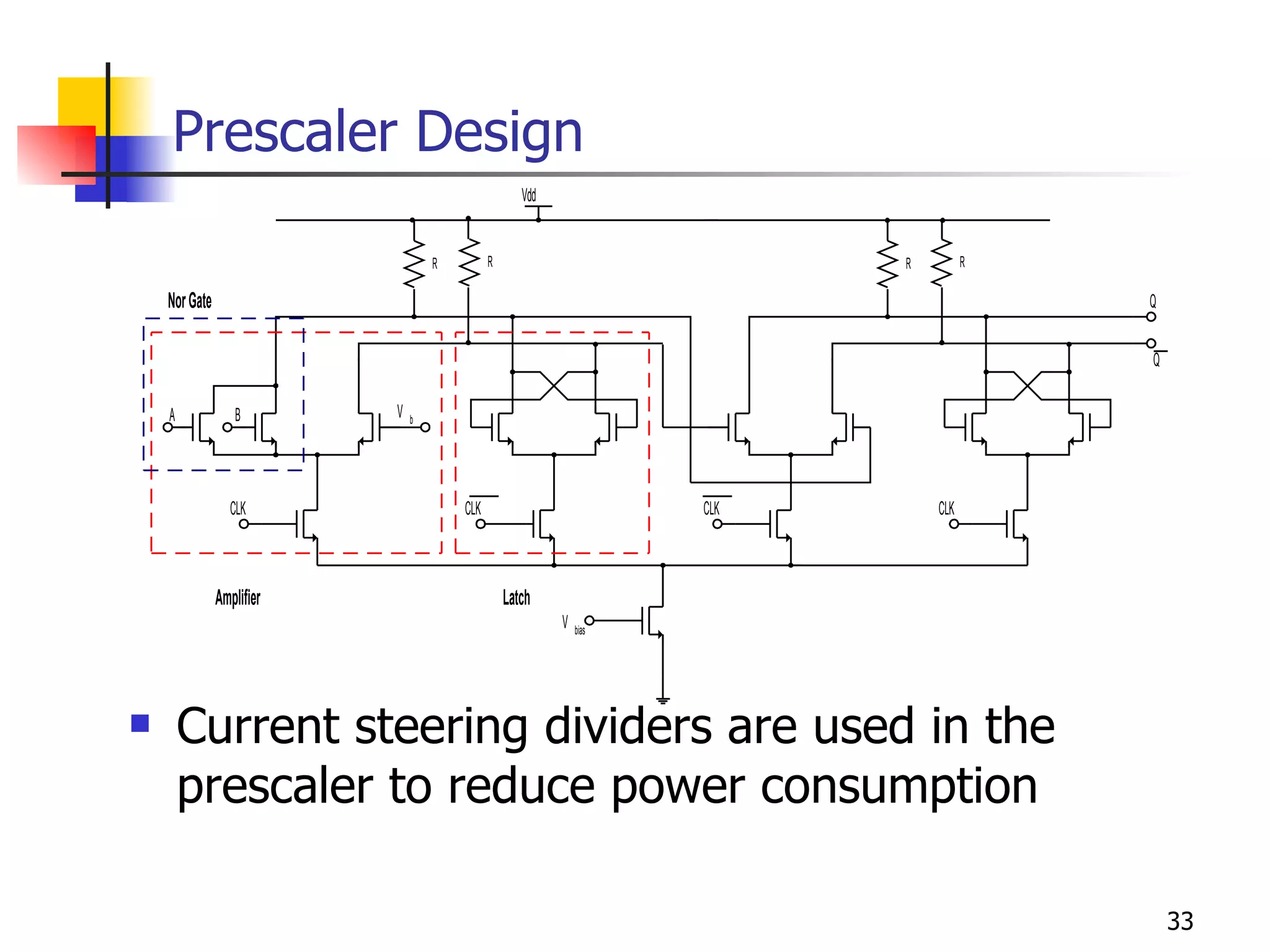
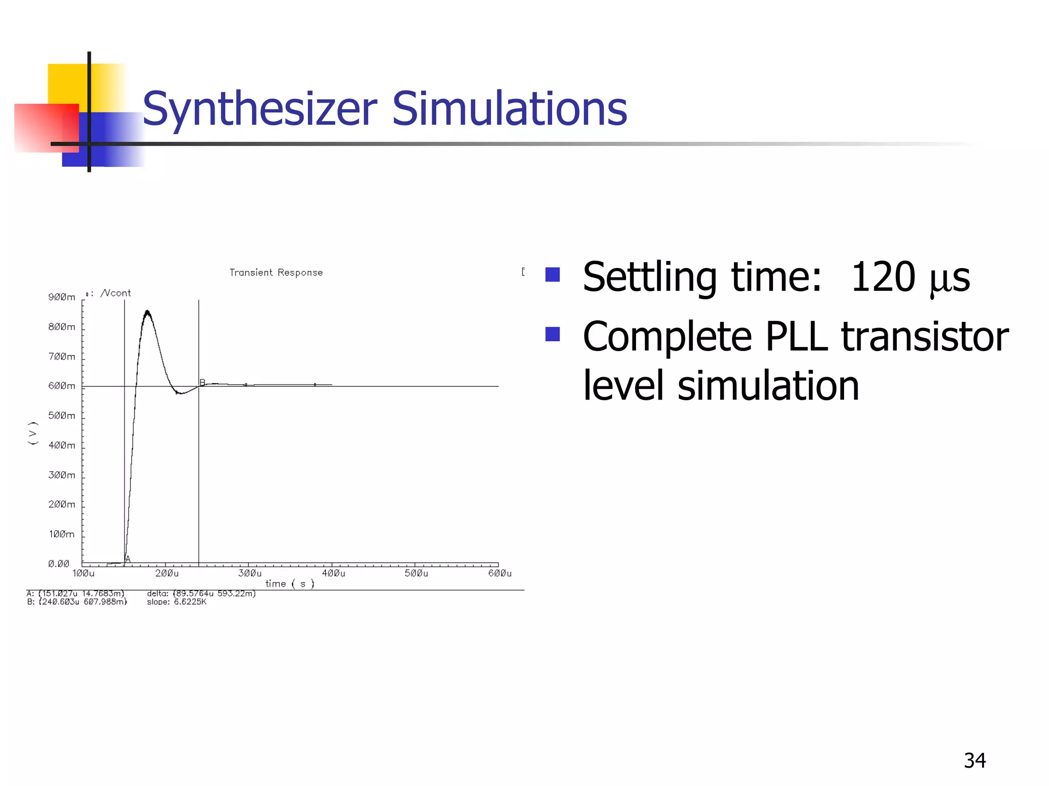
![The Synthesizer Structure An integer N architecture is preferred for the synthesizer to minimize power consumption Current steering logic prescaler Settling time 120 s Phase noise [email_address]](https://image.slidesharecdn.com/rfreceiverdesign-casestudies-110308045151-phpapp01/75/Rf-receiver-design-case-studies-32-2048.jpg)
![Comparison Table 2.5V 1.8V 2.7V Supply voltage 10mm 2 - - - - ADC area (w/ pads) 9mm 2 (w/o ADC) 16mm 2 (transceiver) N/A Rx area (w/ pads) 10dBm 20dBm N/A N/A IIP2 -13dBm -12dBm -8dBm -7dBm IIP3 15.6mA 13.4mA - - - - ADC active current 30mA (w/o ADC) 27.9mA (w/o ADC) 60mA 65mA 46mA Rx active current 0.25m BiCMOS 0.18 m CMOS 0.35 m CMOS Technology -86dBm -91dBm -92dBm (0dB SNR) -80dBm -88dBm -82dbm Sensitivity 6MHz (LPF) 600kHz (LPF) 7.5MHz (LPF) 1MHz (BPF) 7.5MHz (LPF) 1MHz (BPF) Filter bandwidth Included Not included Not included ADC Shared shared separate Baseband amplifier Programmable programmable separate Channel select filter AC coupling Injection at AGC input Programmable loop Offset cancellation DCR DCR DCR Low-IF DCR Low-IF Receiver Architecture Wi-Fi BT WiFi BT WiFi BT This design [2] [1]](https://image.slidesharecdn.com/rfreceiverdesign-casestudies-110308045151-phpapp01/75/Rf-receiver-design-case-studies-86-2048.jpg)
![Refer ences [1] W. Sheng, B. Xia, A.E.Emira, C. Xin, A.Y. Valero-Lopez, S.T. Moon, and E. Sanchez-Sinencio, “ A 3-V, 0.35 um CMOS Bluetooth Receiver IC ,” IEEE J. of Solid-State Circuits , Vol. 38, pp. 30-42, January 2003 [2] B. Xia, C. Xin, W. Sheng, A.Y. Valero-Lopez, and E. Sanchez-Sinencio, “ A GFSK Demodulator for Low-IF Bluetooth Receiver,” IEEE J. Solid-State Circuits , Vol. 38, pp. 1397-1400, August 2003. [3] A.A Emira,.; E.Sánchez-Sinencio, “A pseudo differential complex filter for Bluetooth with frequency tuning” IEEE Circuits and Systems II ,Volume: 50, pp. 742 - 754 Oct. 2003 [4] K. Shu, E. Sanchez-Sinencio, J. Silva-Martinez, S.H.K. Embabi, S.H” A 2.4-GHz monolithic fractional-N frequency synthesizer with robust phase-switching prescaler and loop capacitance multiplier. “ IEEEJ. of Solid-State Circuits , Vol. 38 , pp. 866-874, June 2003. [5] A. Emira, A. Valdes-Garcia, B. Xia, A. Mohieldin, A. Valero-Lopez, S. Moon, C. Xin, and E. Sánchez-Sinencio, “A Dual-Mode 802.11b/Bluetooth Receiver in 0.25mm BiCMOS,” IEEE International Solid-State Circuits Conference (ISSCC)I, pp. 270-271,527, Wireless Consumer Papers, San Francisco, CA, February 2004.](https://image.slidesharecdn.com/rfreceiverdesign-casestudies-110308045151-phpapp01/75/Rf-receiver-design-case-studies-88-2048.jpg)

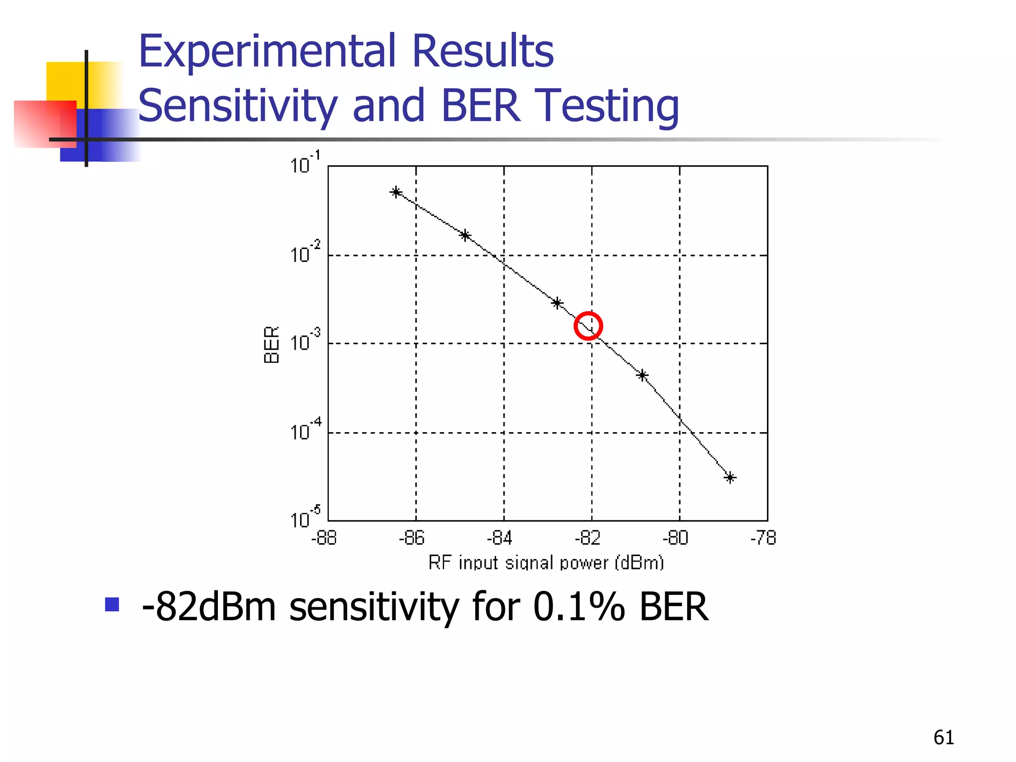
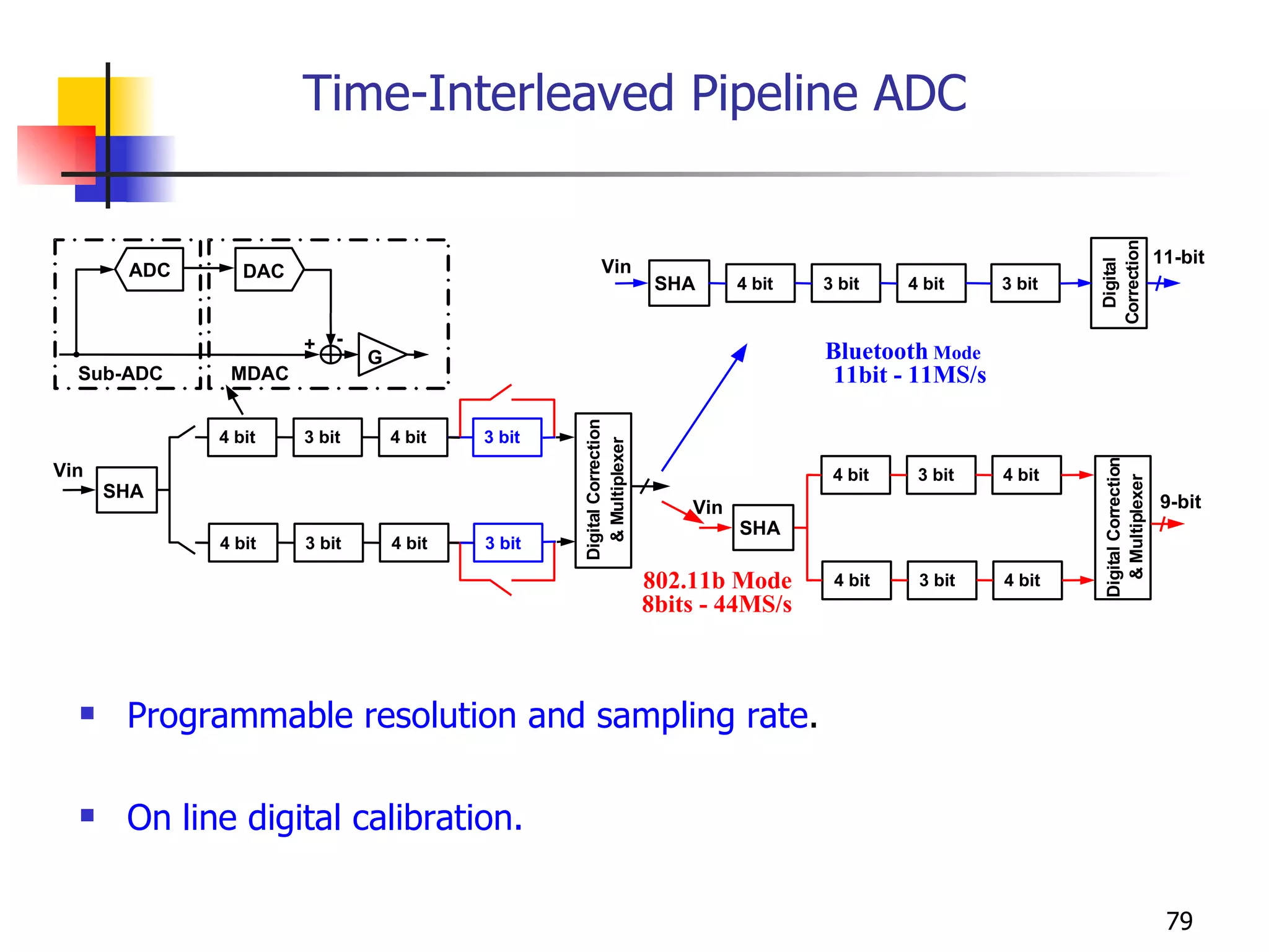
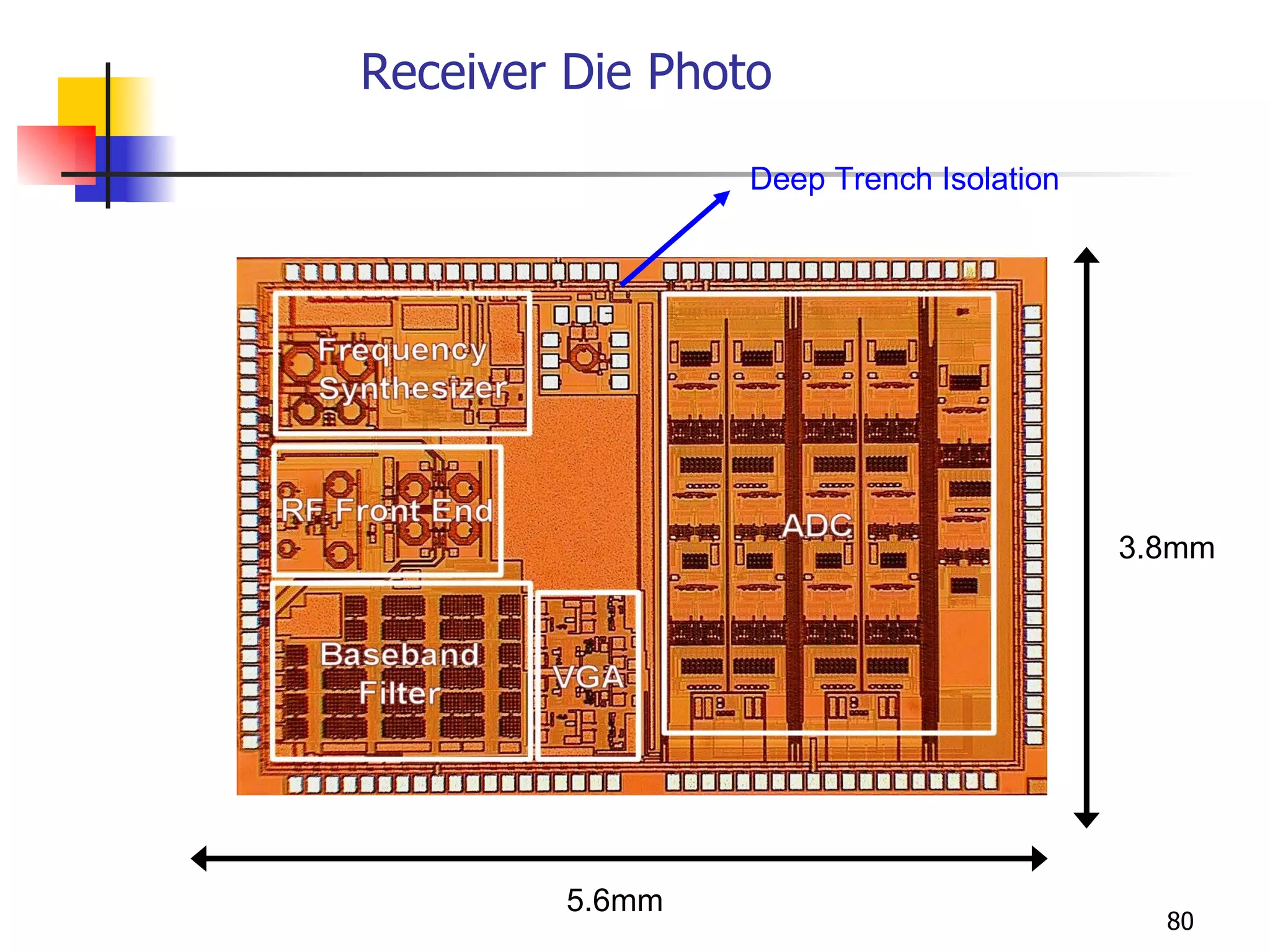
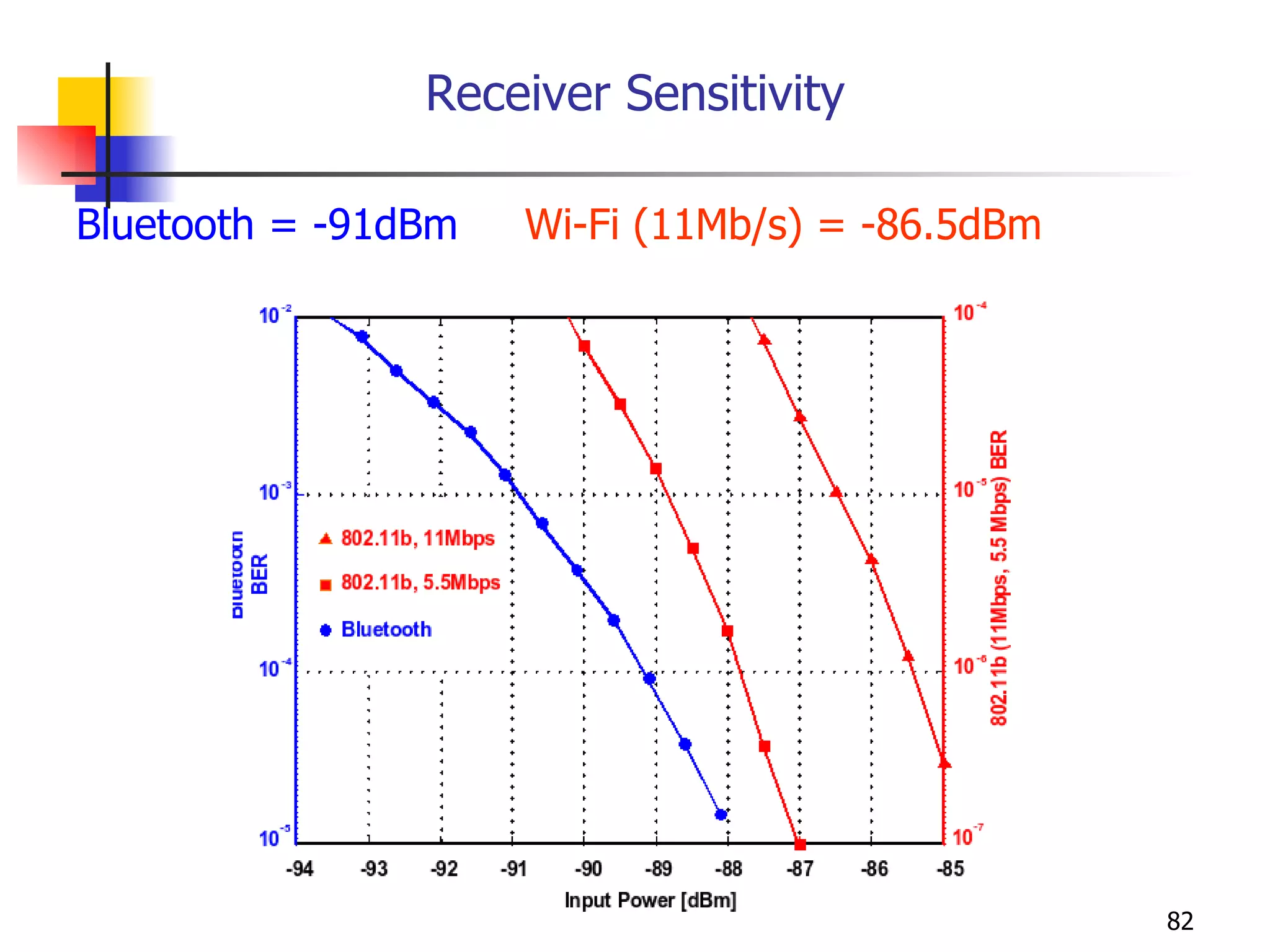
The document describes several receiver designs developed at the Analog and Mixed-Signal Center between 2000-2008, including a Bluetooth receiver, a dual-standard Bluetooth/Wi-Fi receiver ("Chameleon" receiver), and others. It provides details on the system design and individual building blocks for the Bluetooth and Chameleon receivers, such as the low-IF architecture, active complex filter, GFSK demodulator, and time-interleaved pipeline ADC. Experimental results showed the Bluetooth receiver achieved -82dBm sensitivity while the Chameleon receiver achieved -91dBm and -86.5dBm for Bluetooth and Wi-Fi modes respectively.
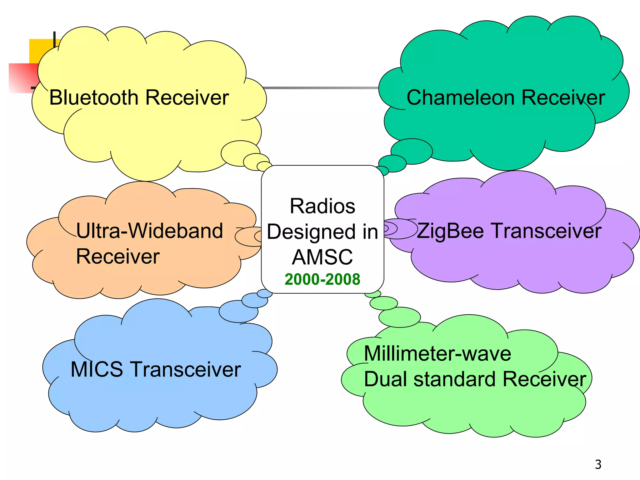
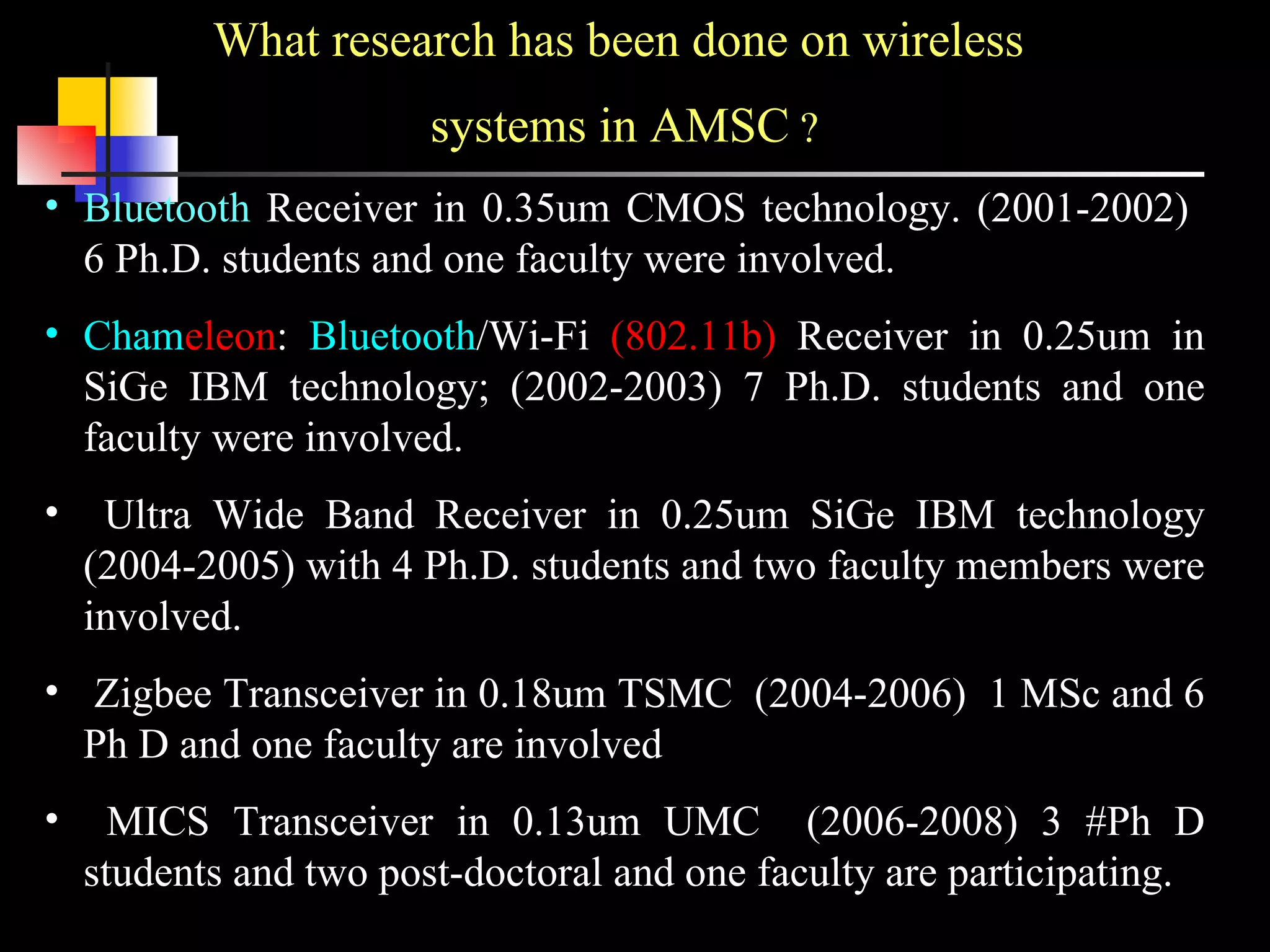
Introduction to receiver design case studies at AMSC, covering Bluetooth, ZigBee, and other technology advancements from 2000-2008.
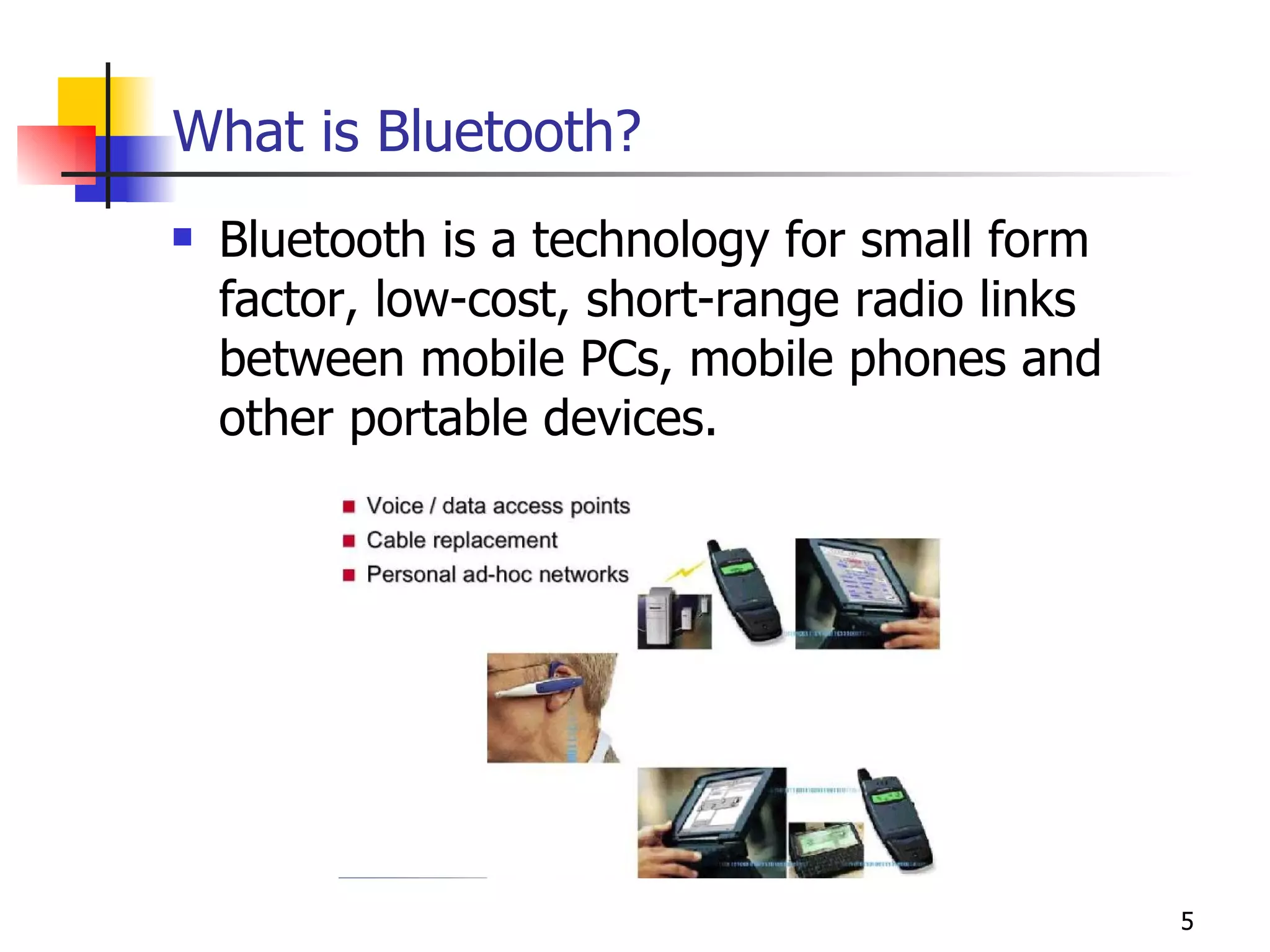
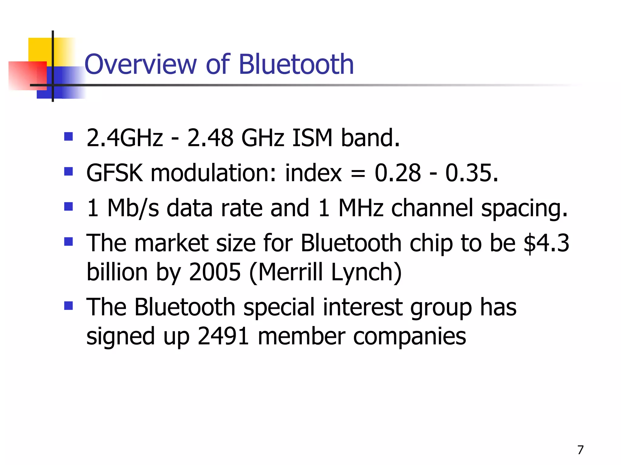
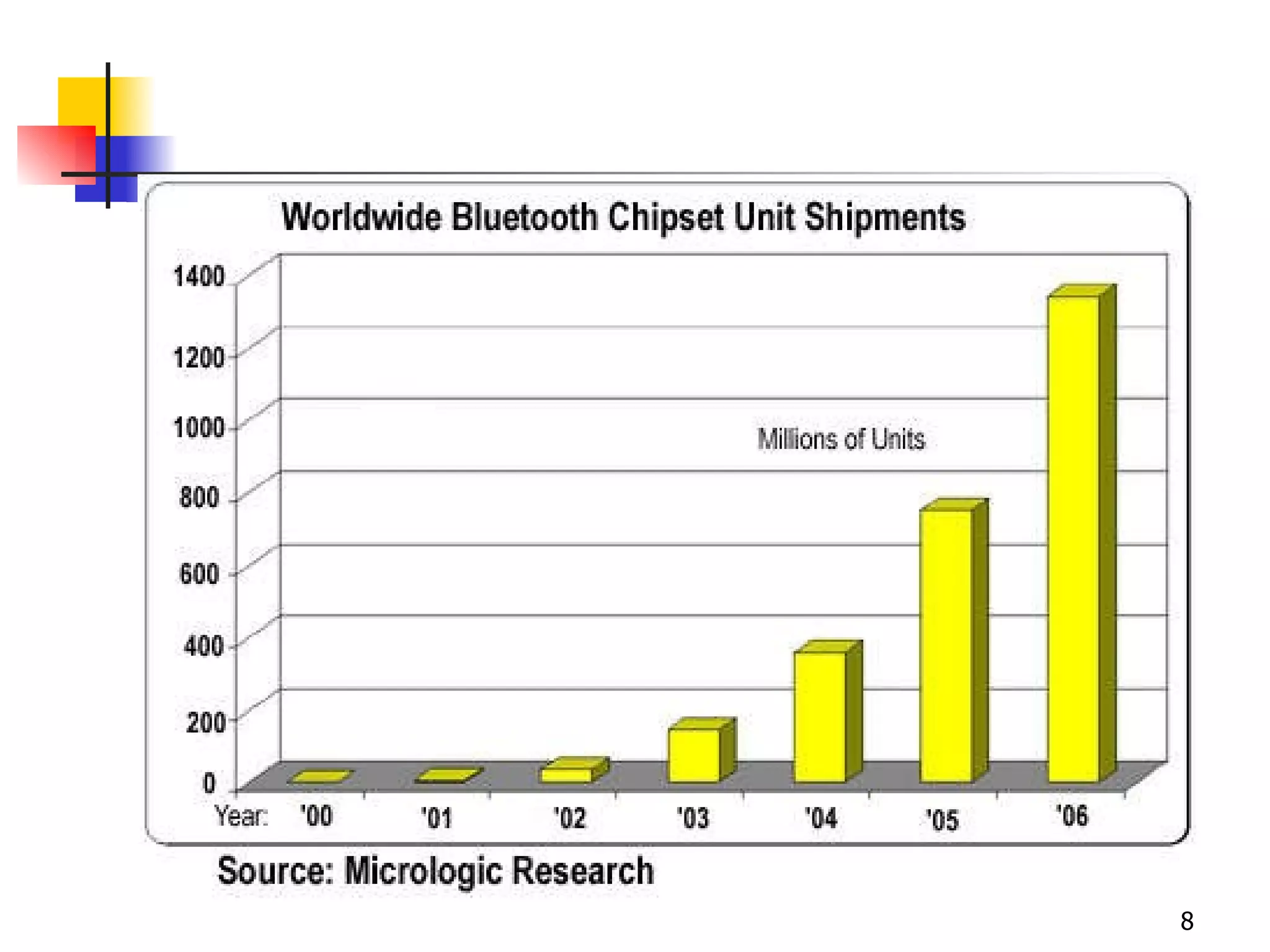
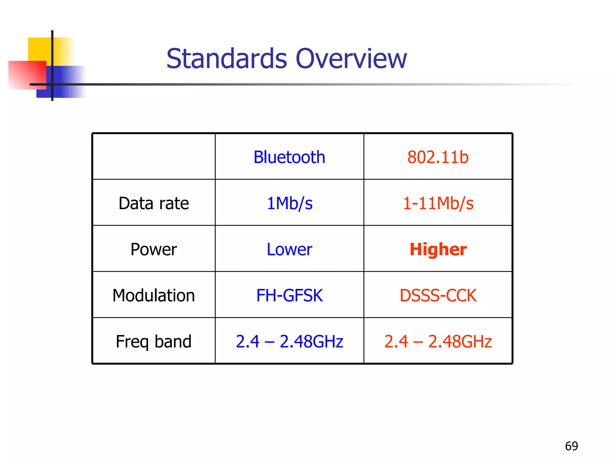
Explanation of Bluetooth technology, its relevant frequency, modulation, data rate, and market size projections by 2005.
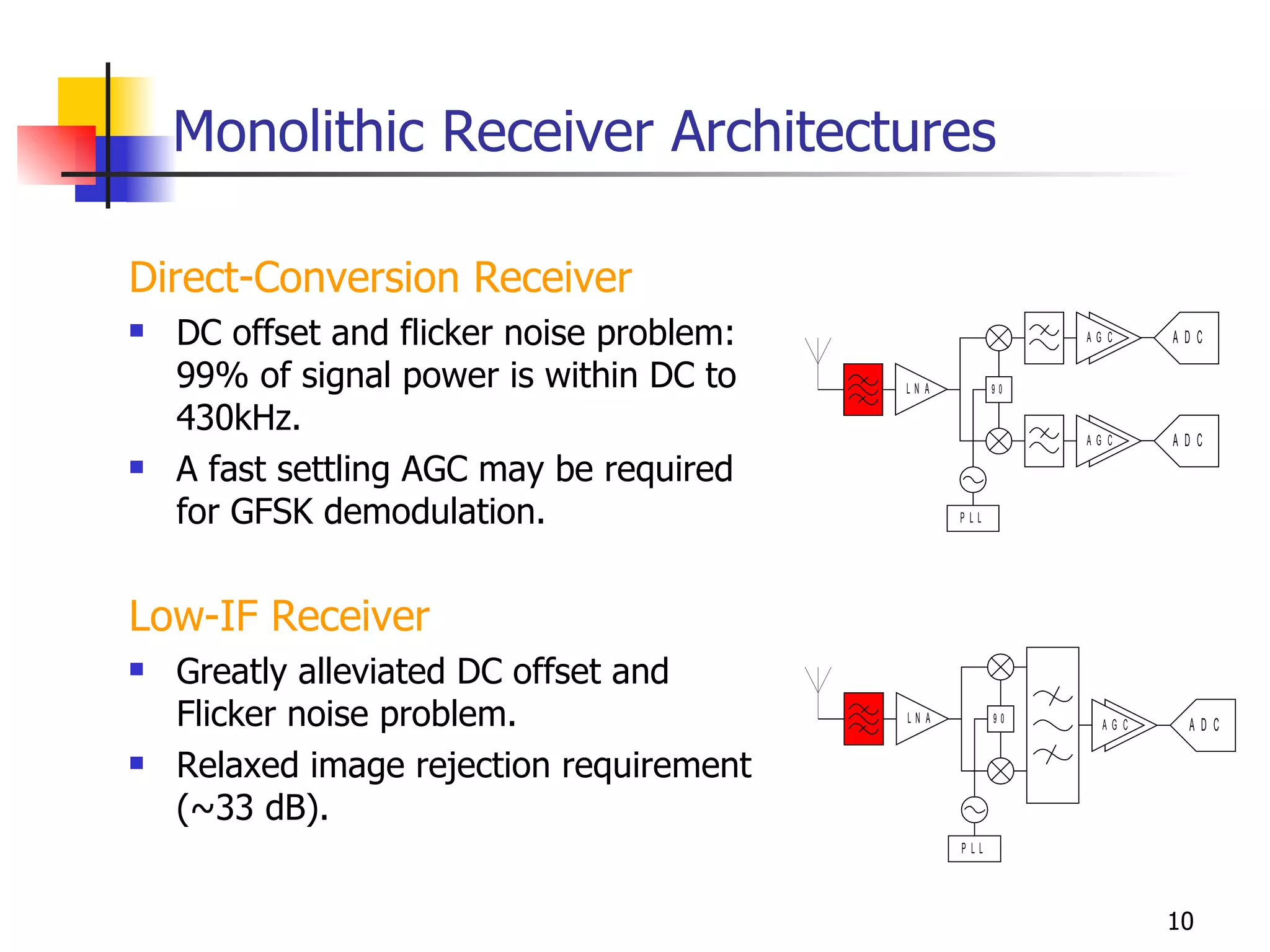
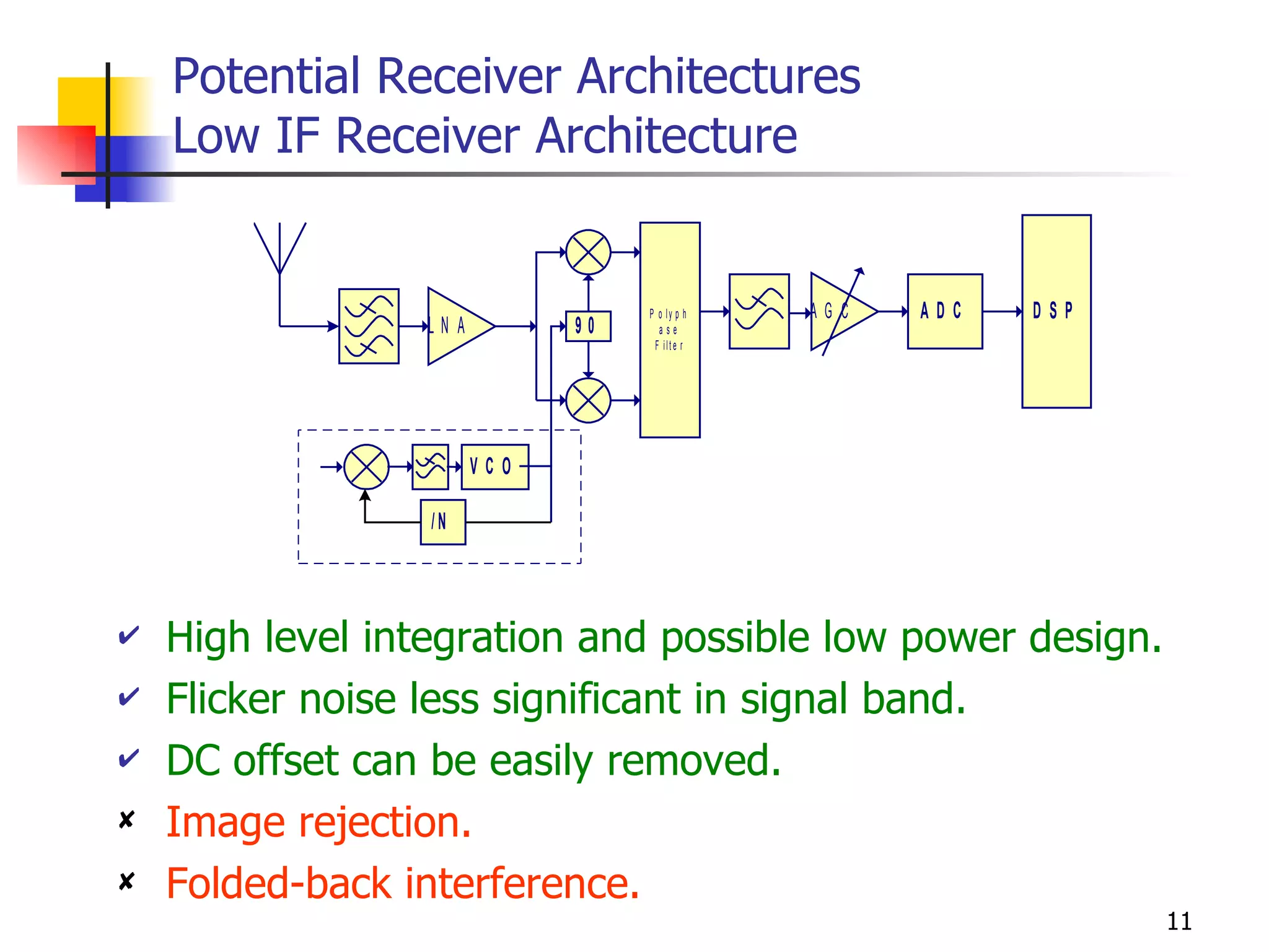
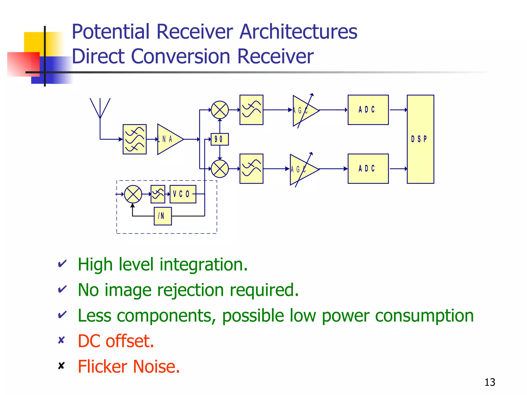
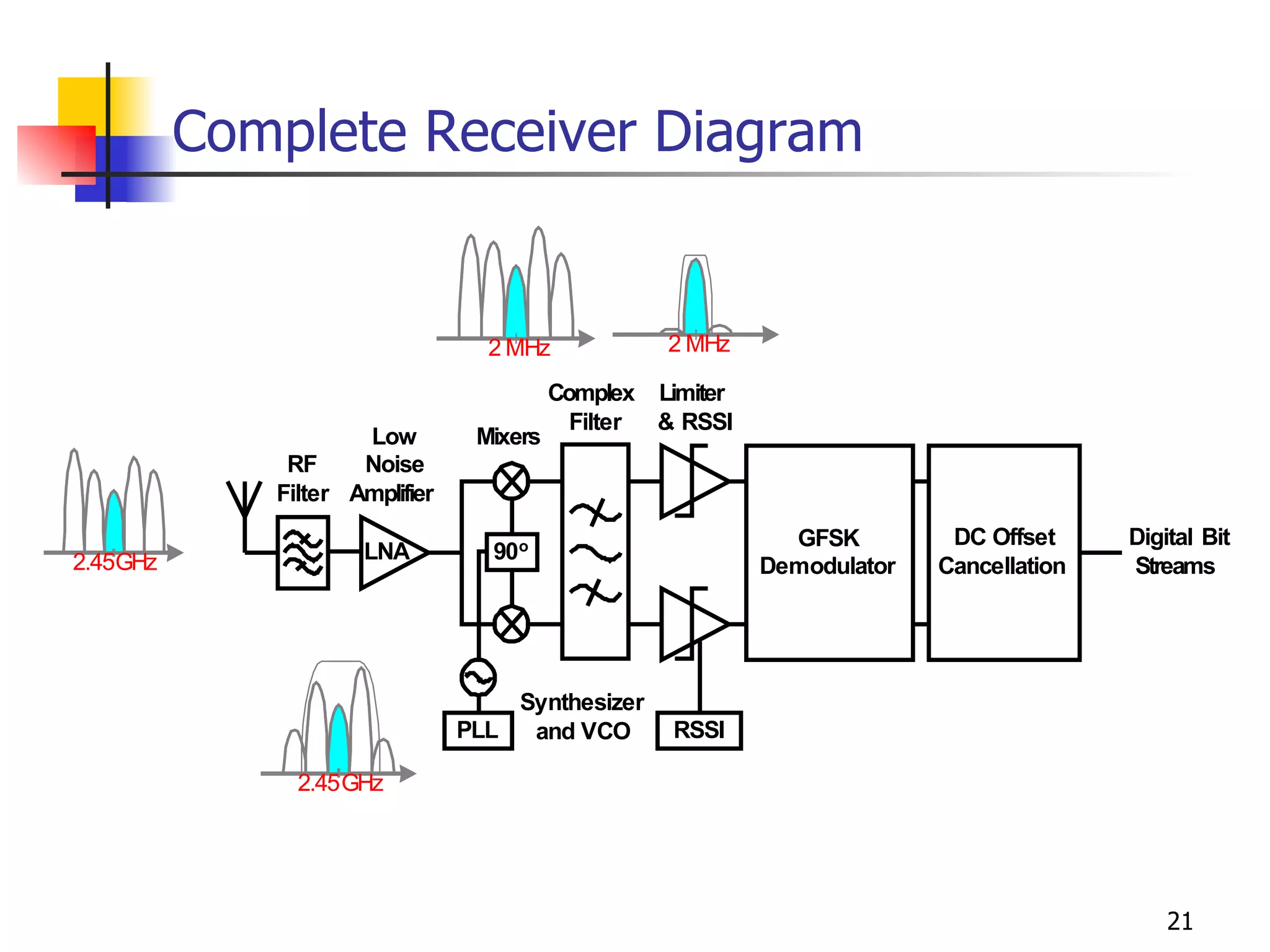
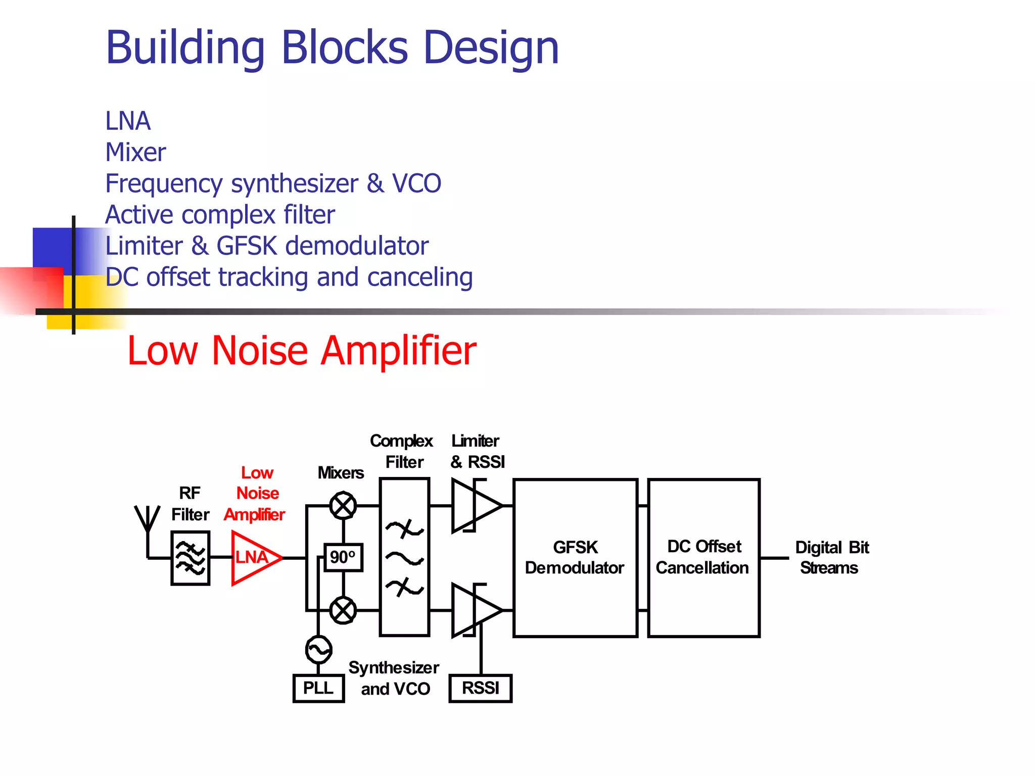
Exploring monolithic architectures, direct conversion, and low-IF receivers, addressing their noise issues and integration benefits.
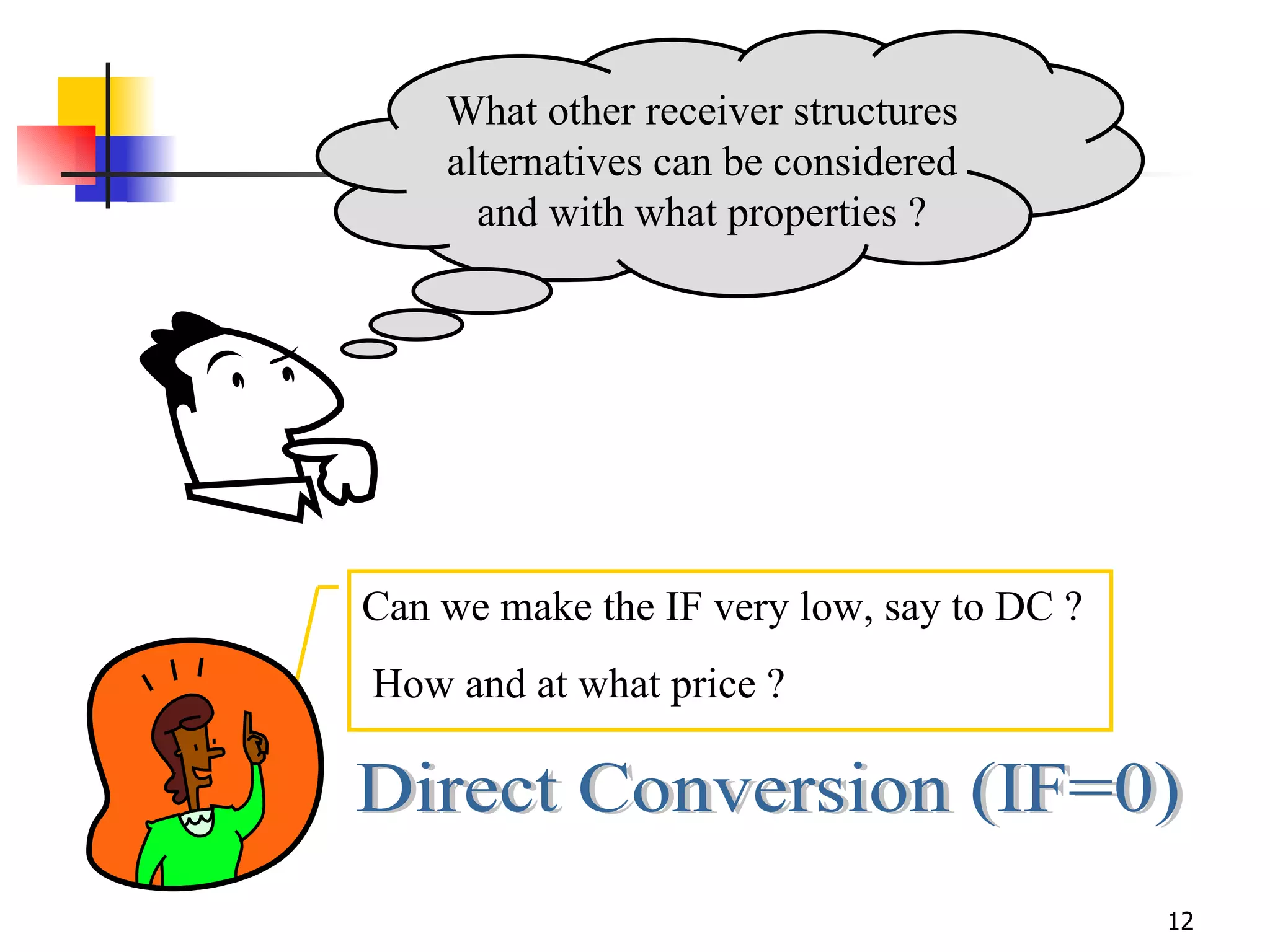
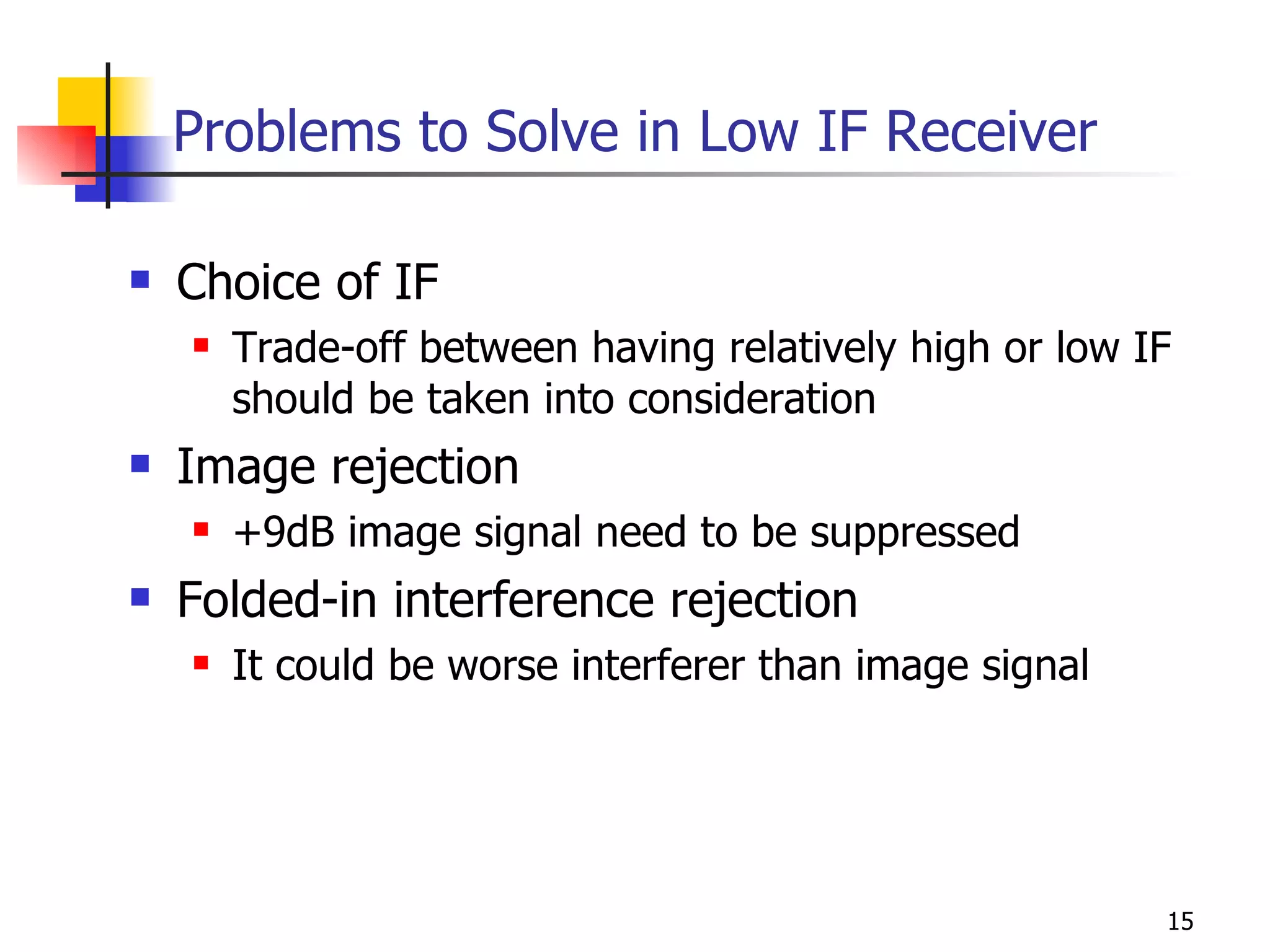
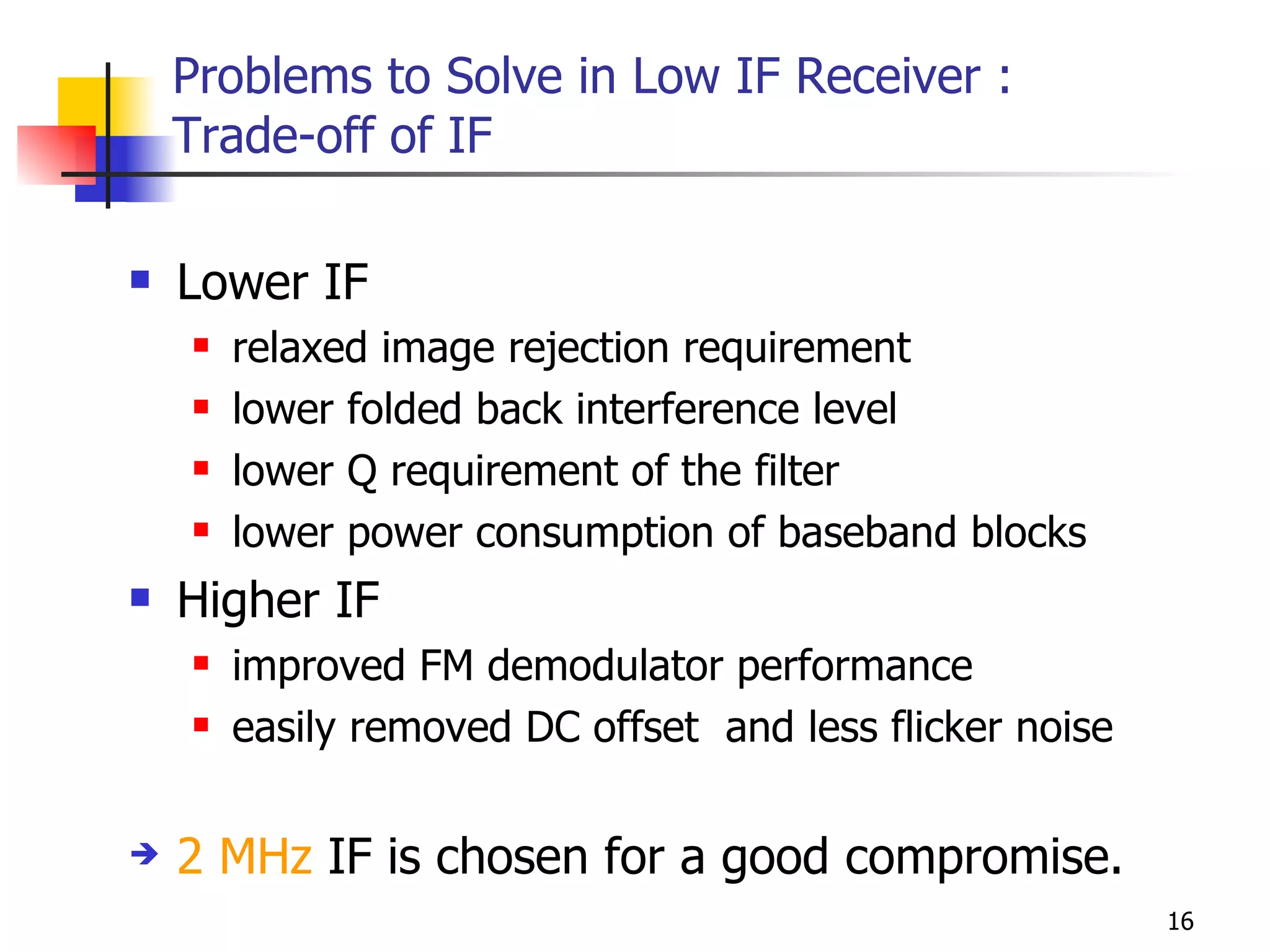
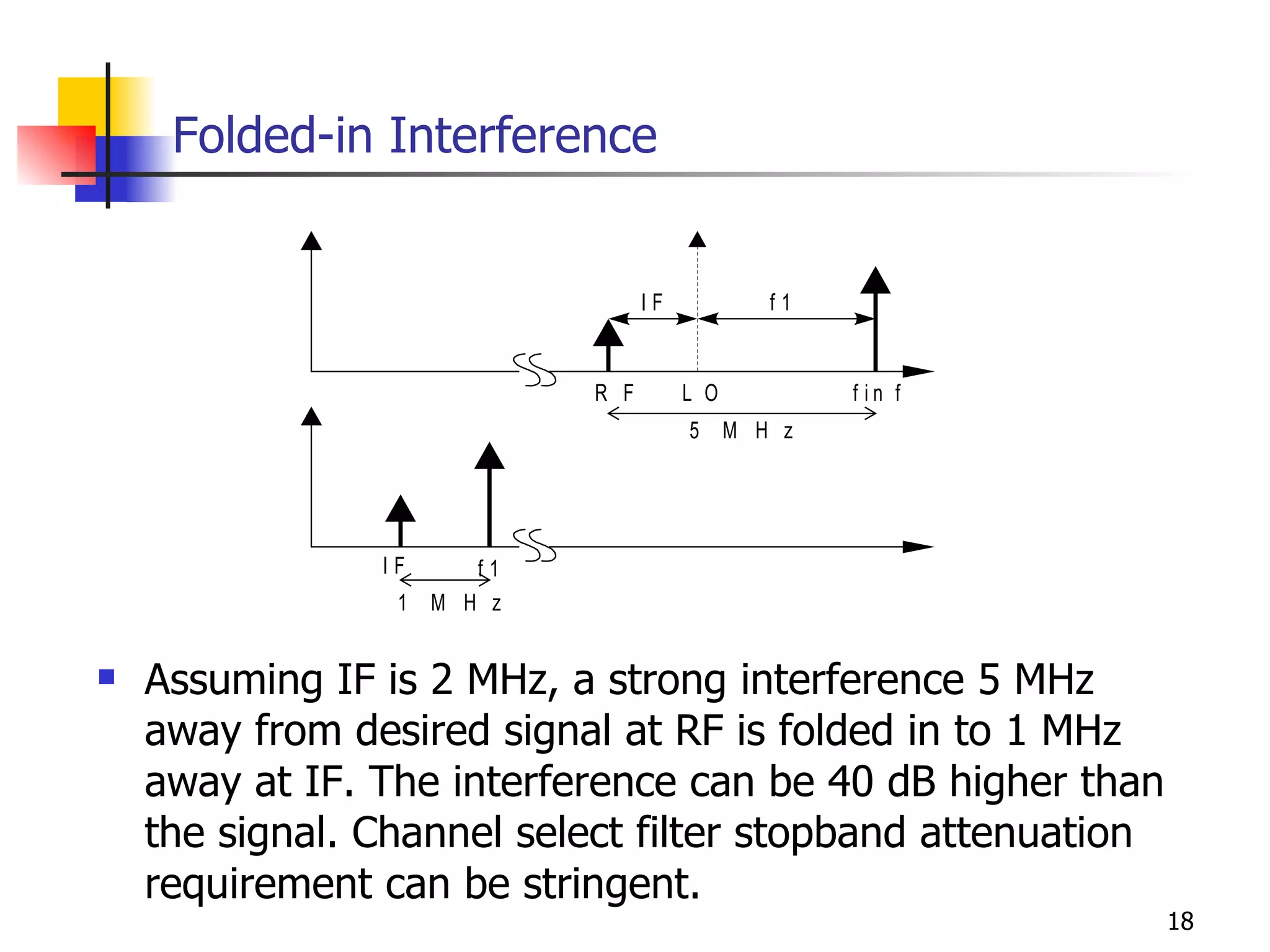
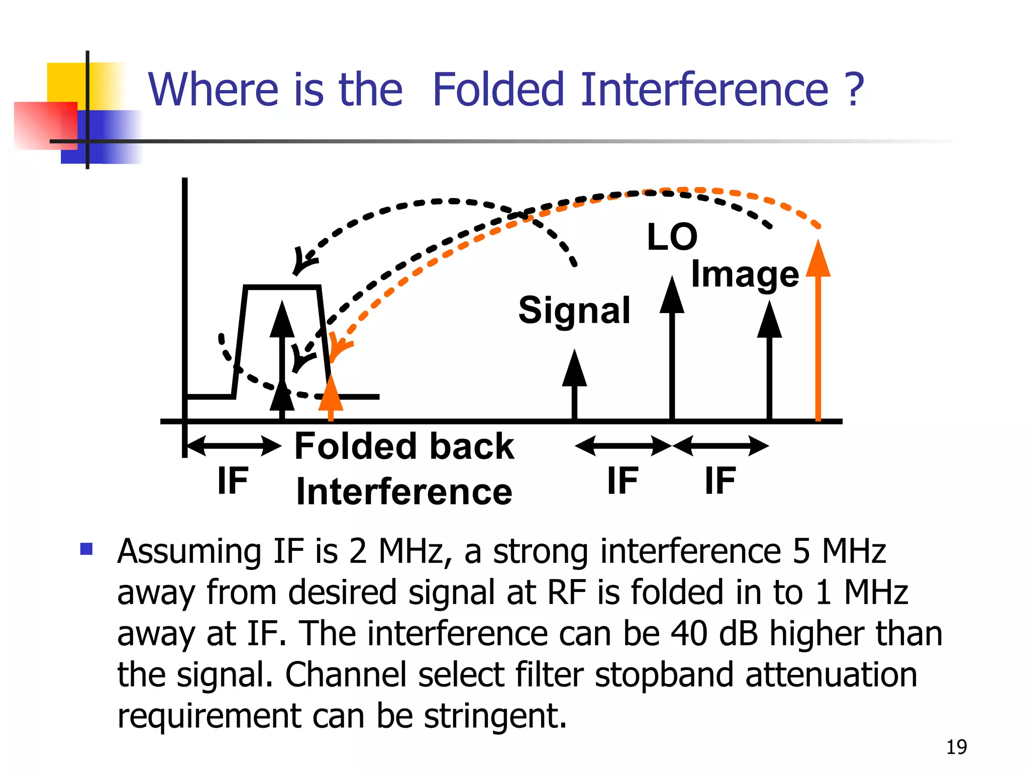
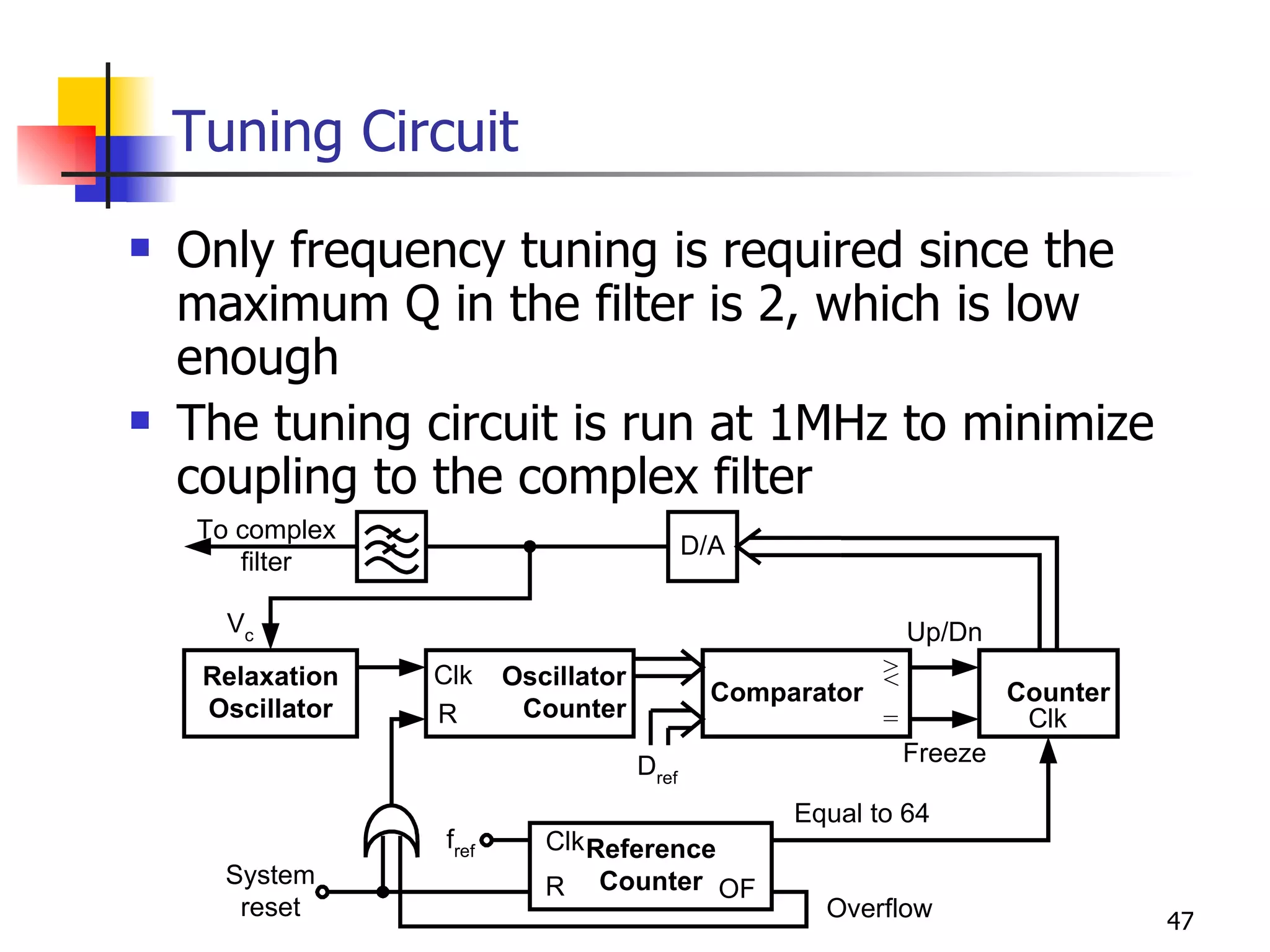
Challenges in choosing IF for low-IF receivers and performance trade-offs, aiming for optimal noise and power requirements.
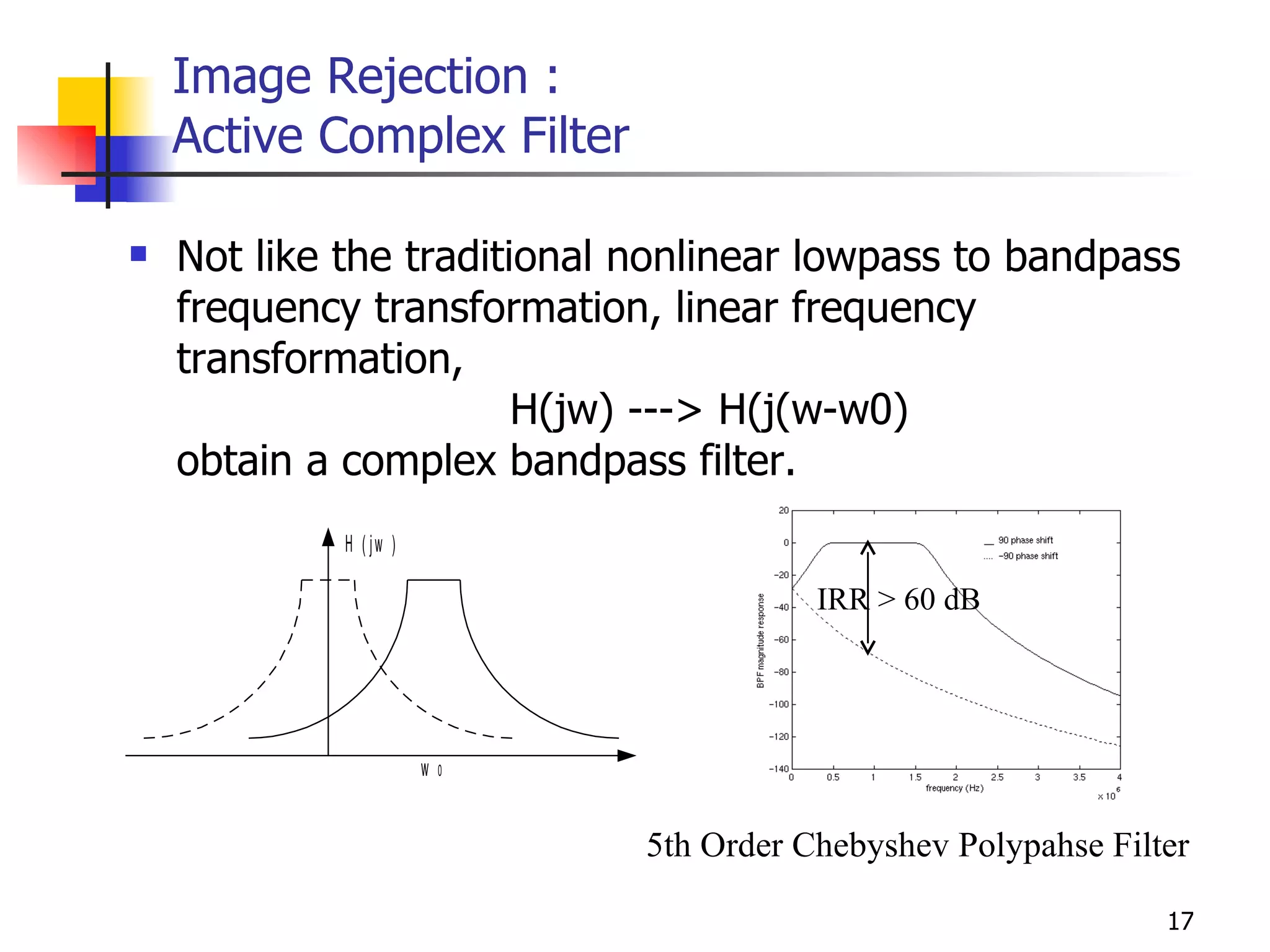
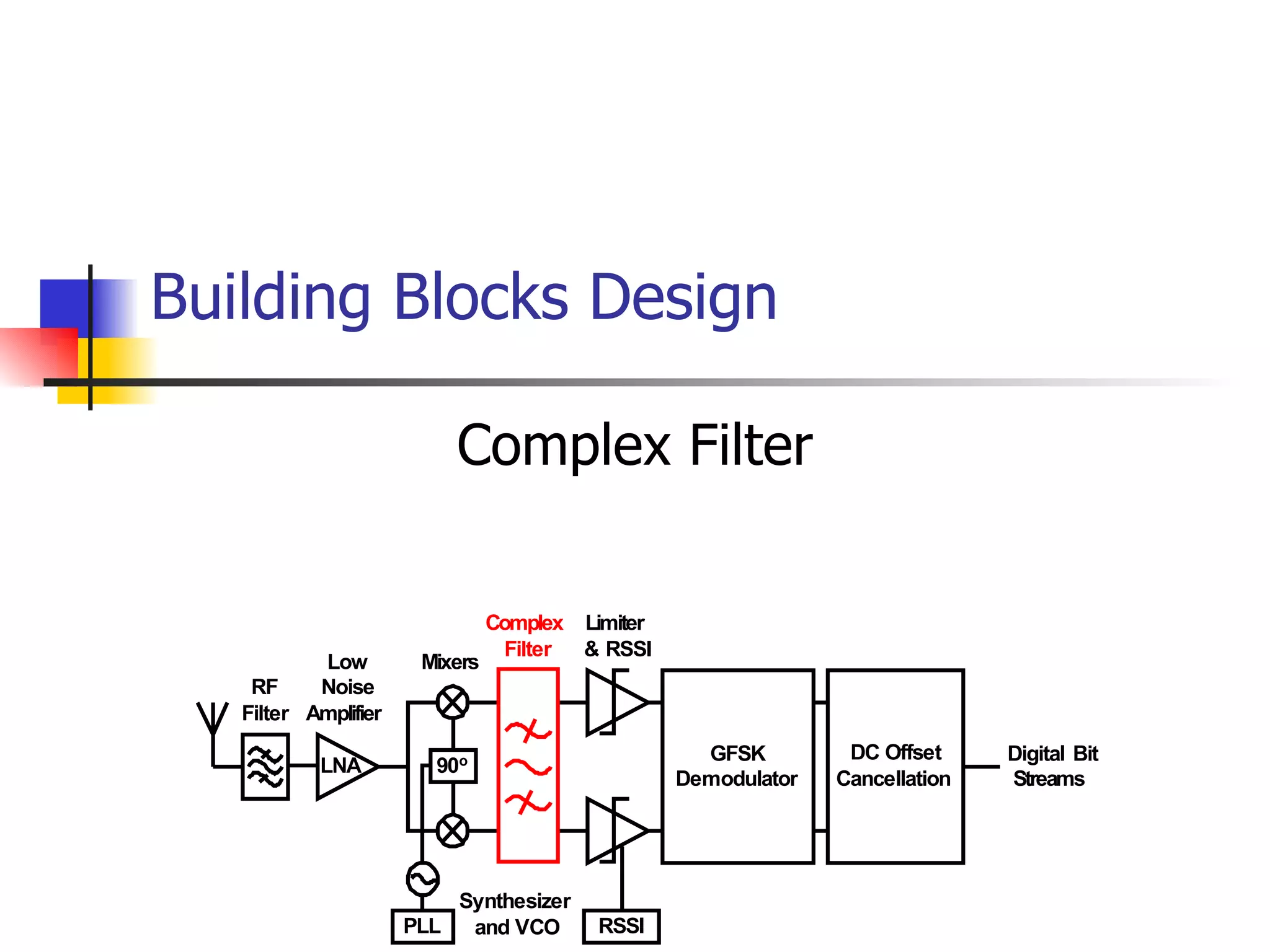
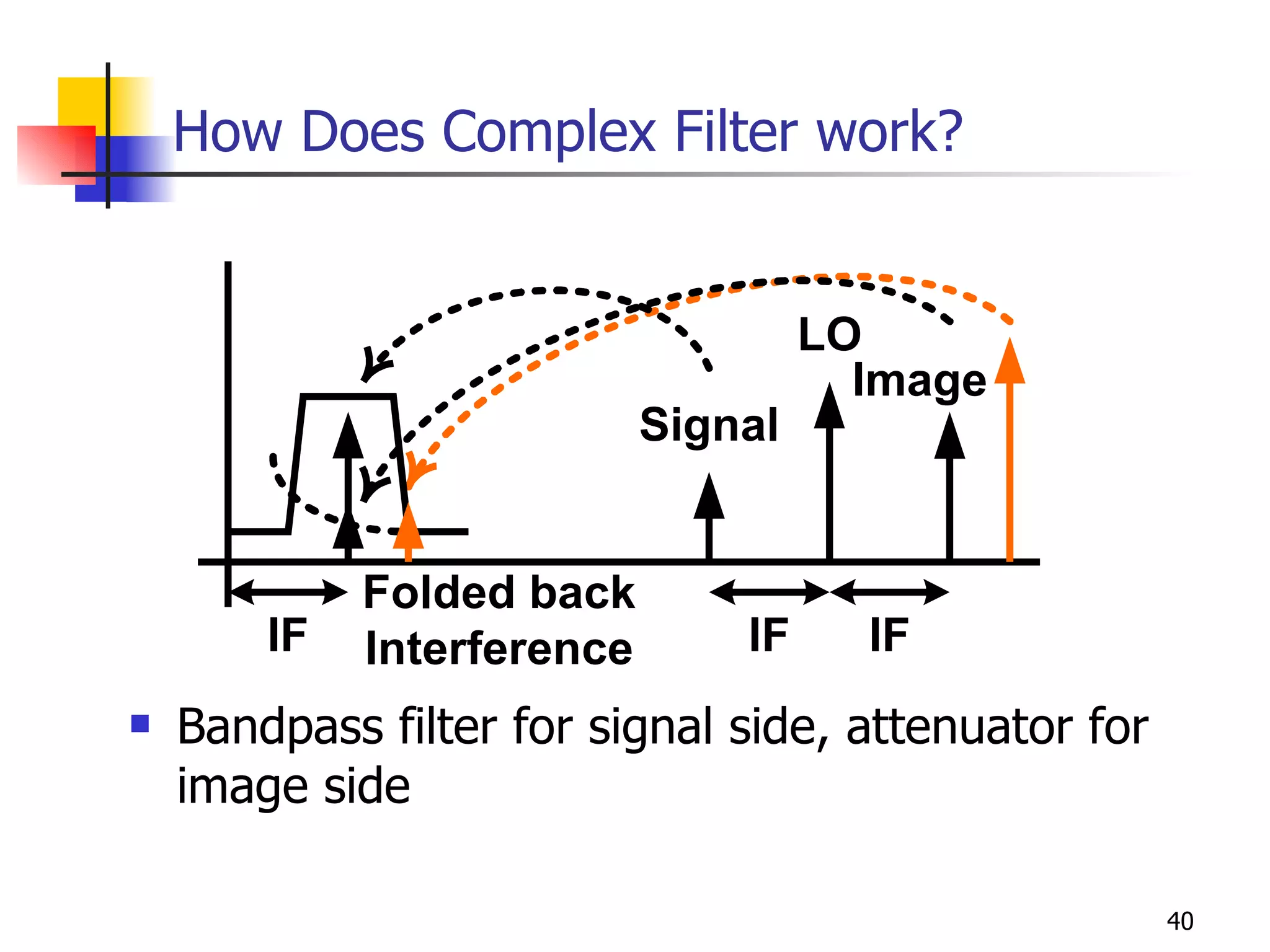
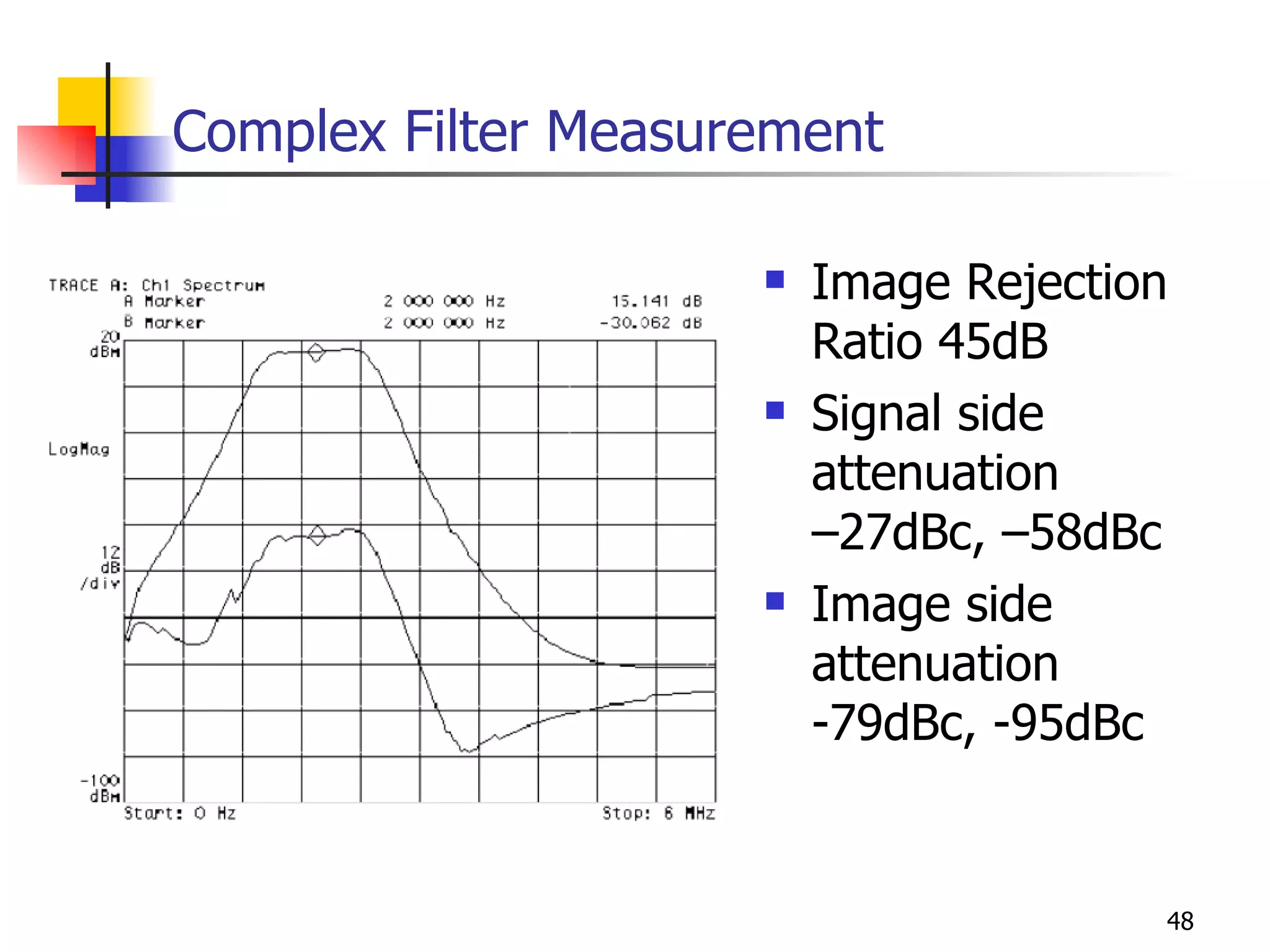
Active complex filter and interference management strategies, focusing on image rejection and folded interference issues.
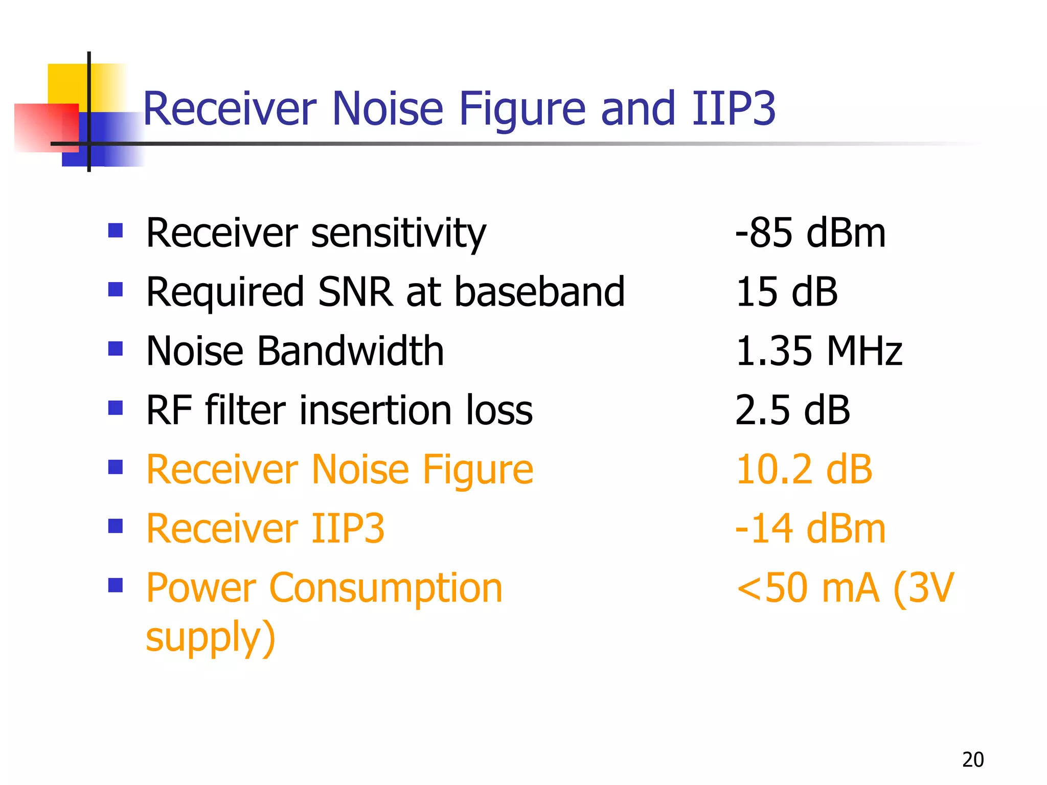
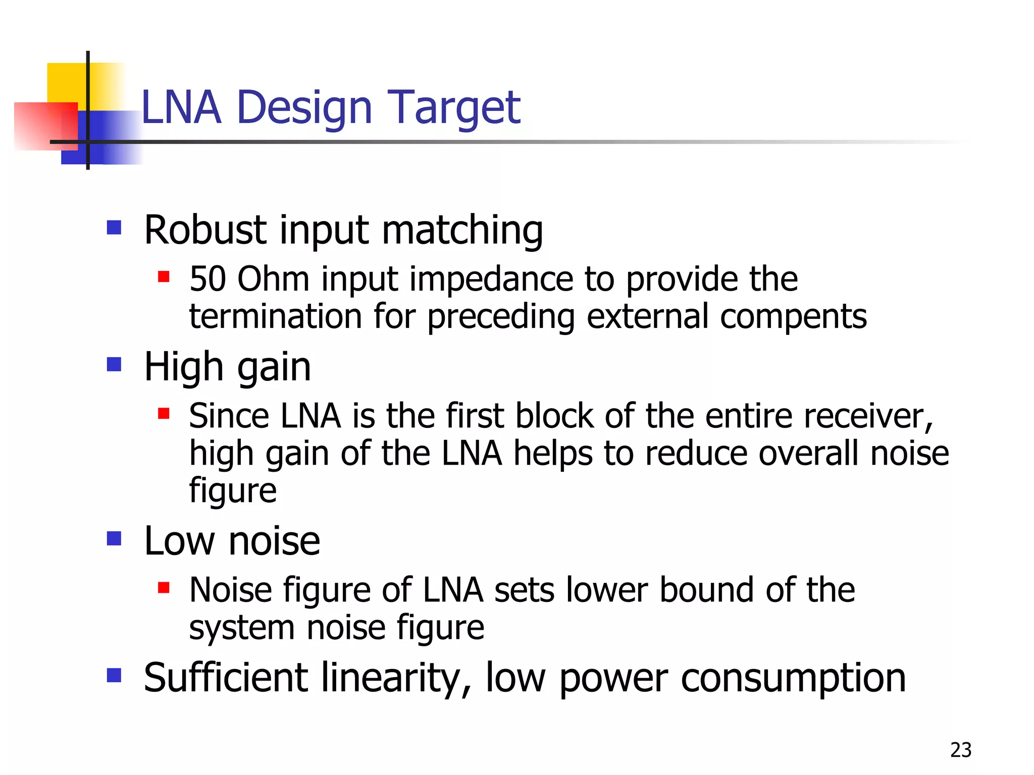
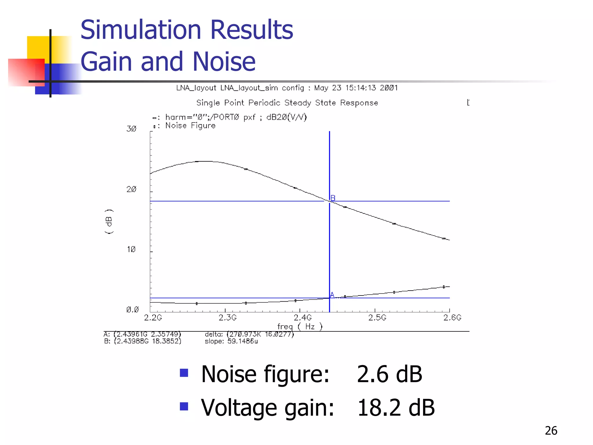
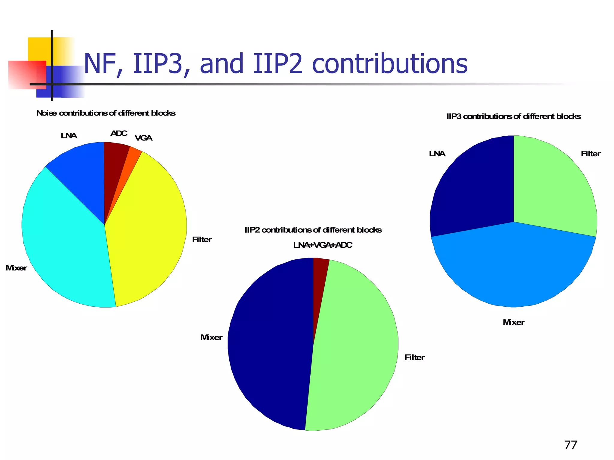
Noise figure, IIP3, and essential performance benchmarks for the receiver components, including LNA and other building blocks.
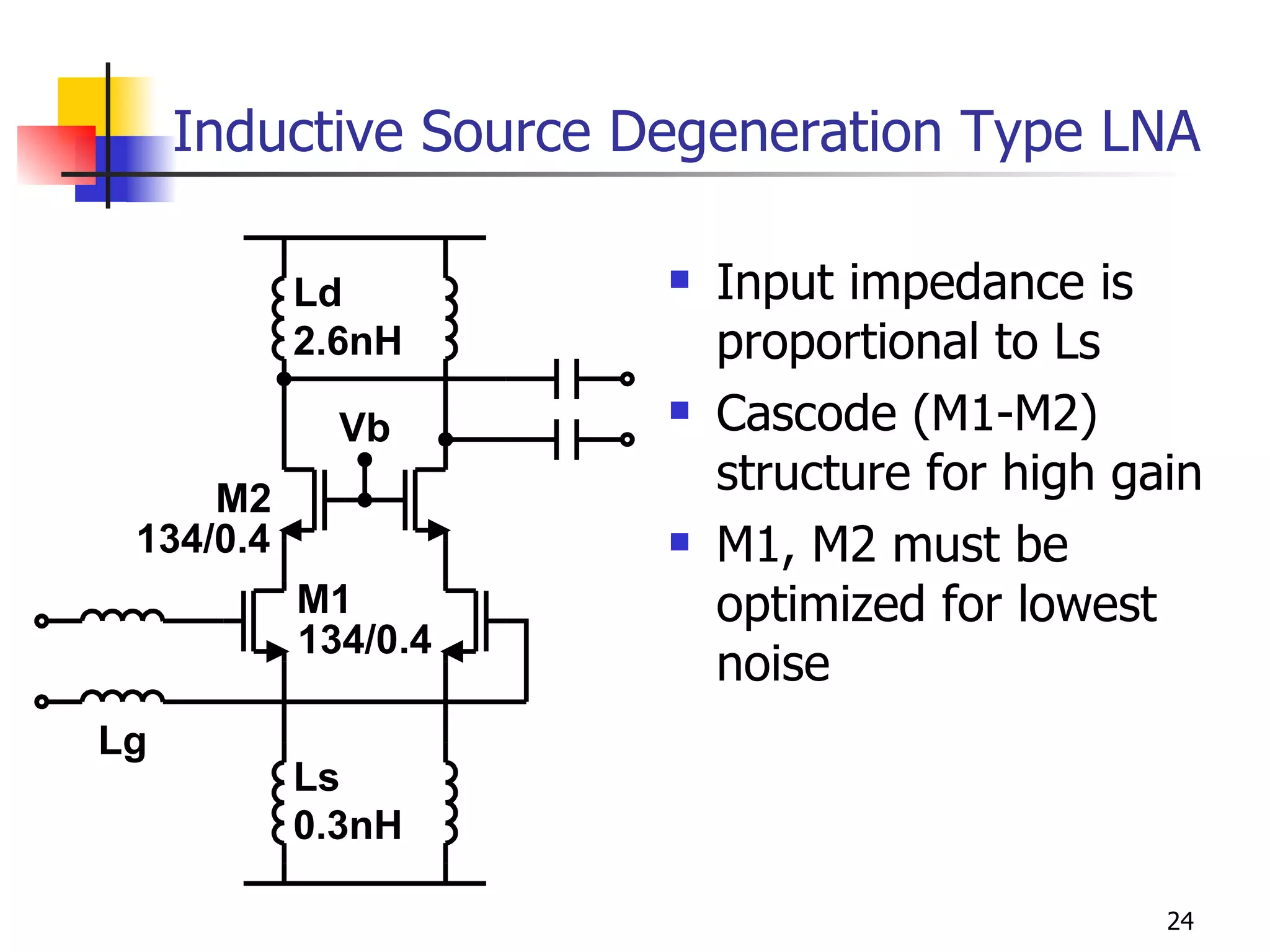
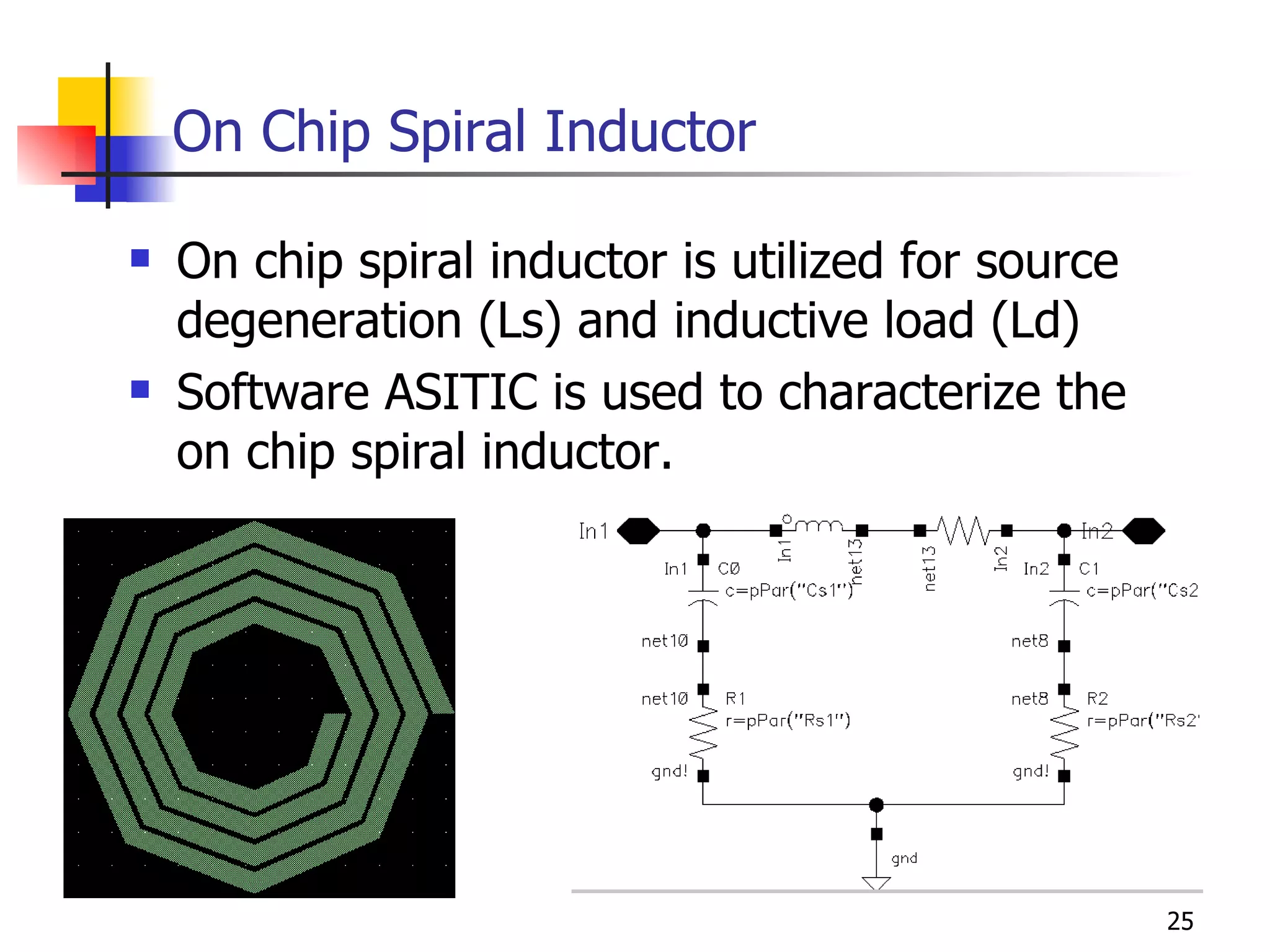
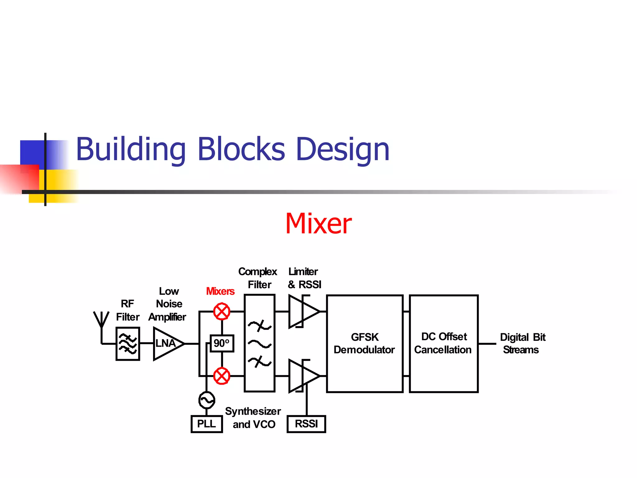
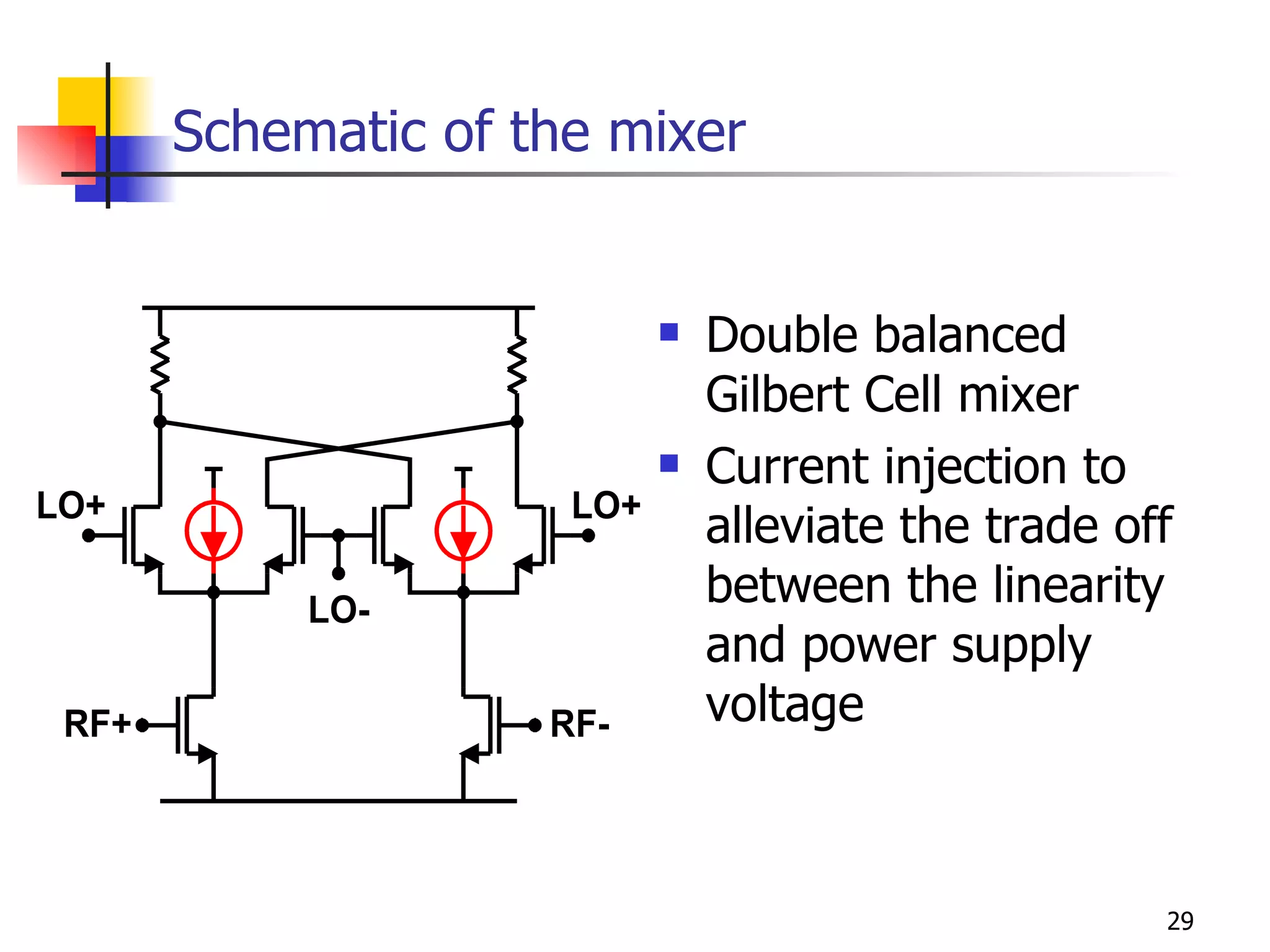
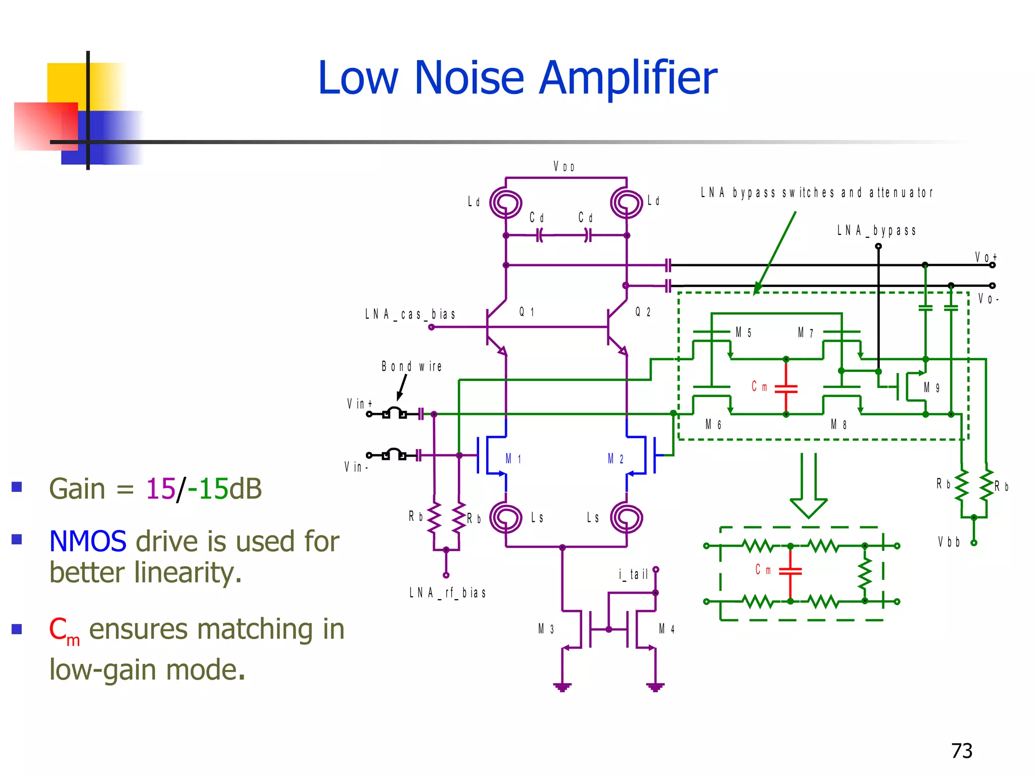
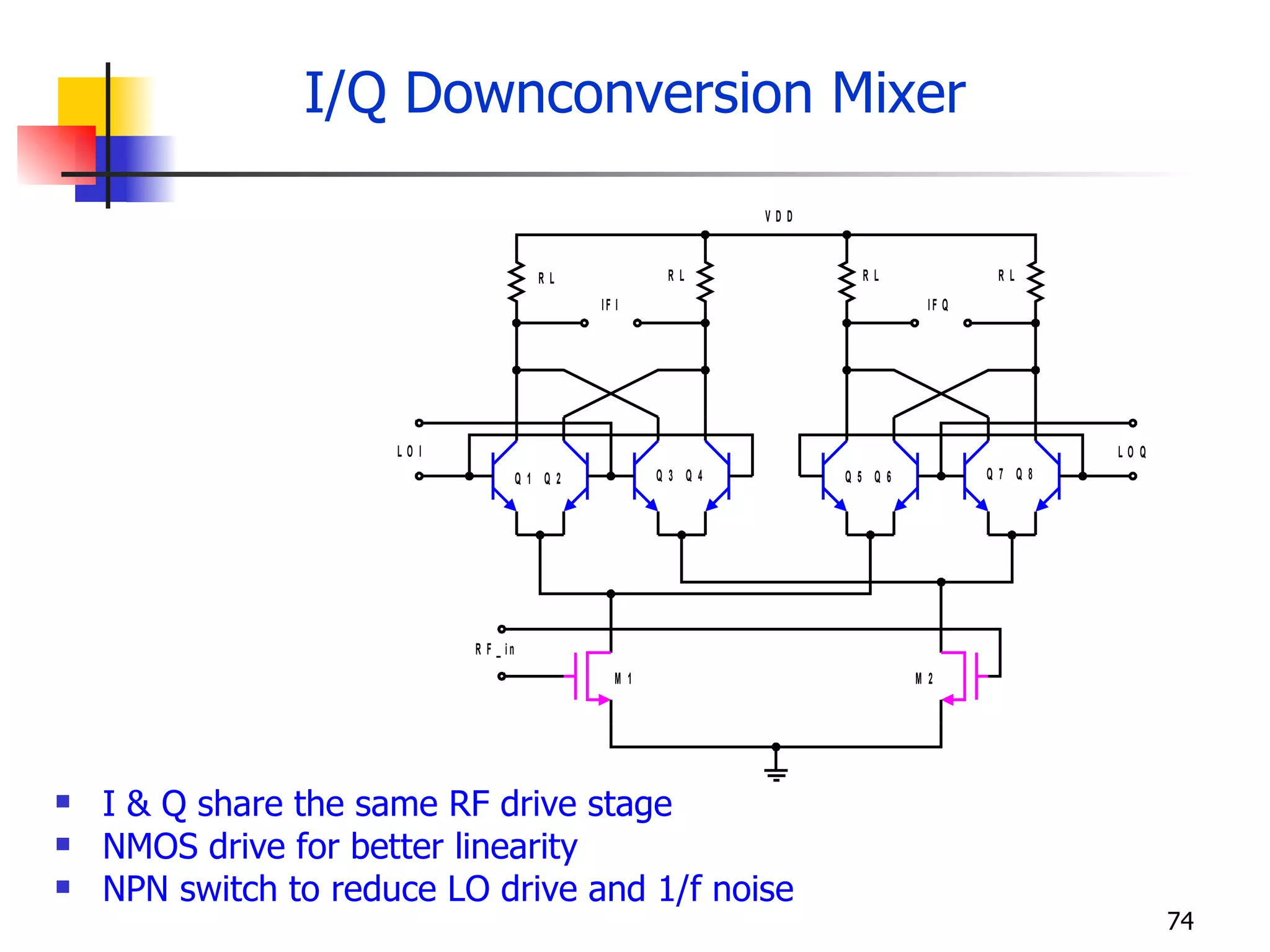
In-depth design considerations for Low Noise Amplifiers (LNA) and mixers targeting low power, high performance.
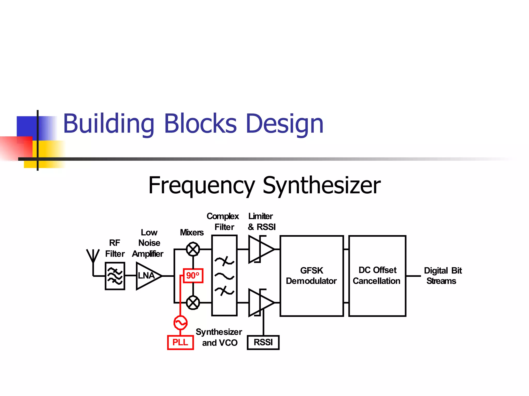
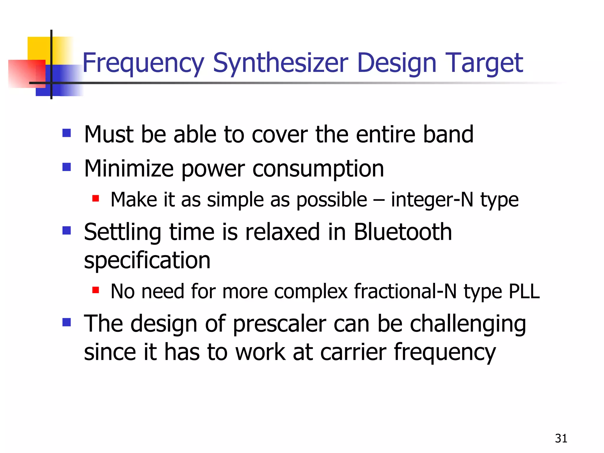
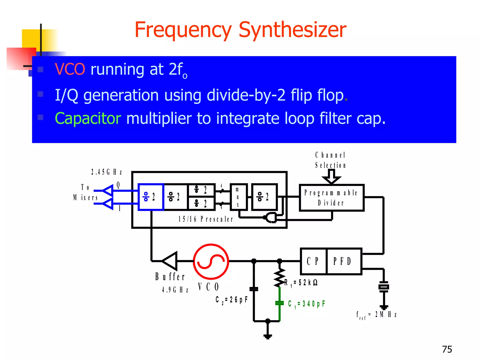
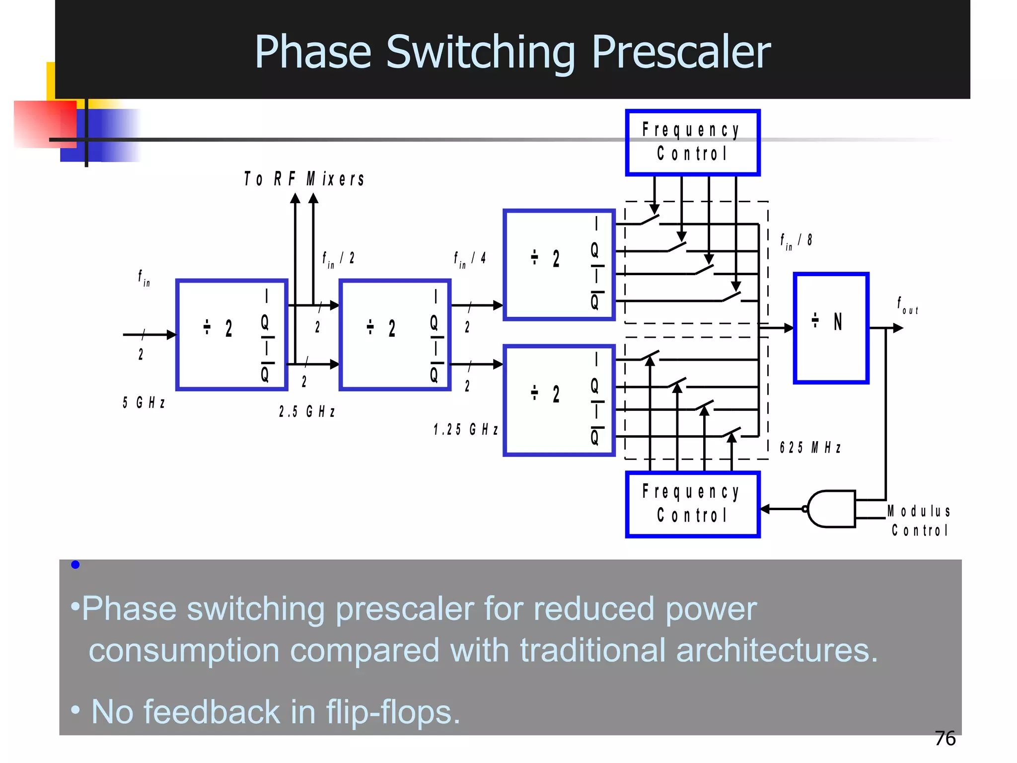
Design objectives and architecture for the frequency synthesizer, focusing on power consumption and frequency coverage.
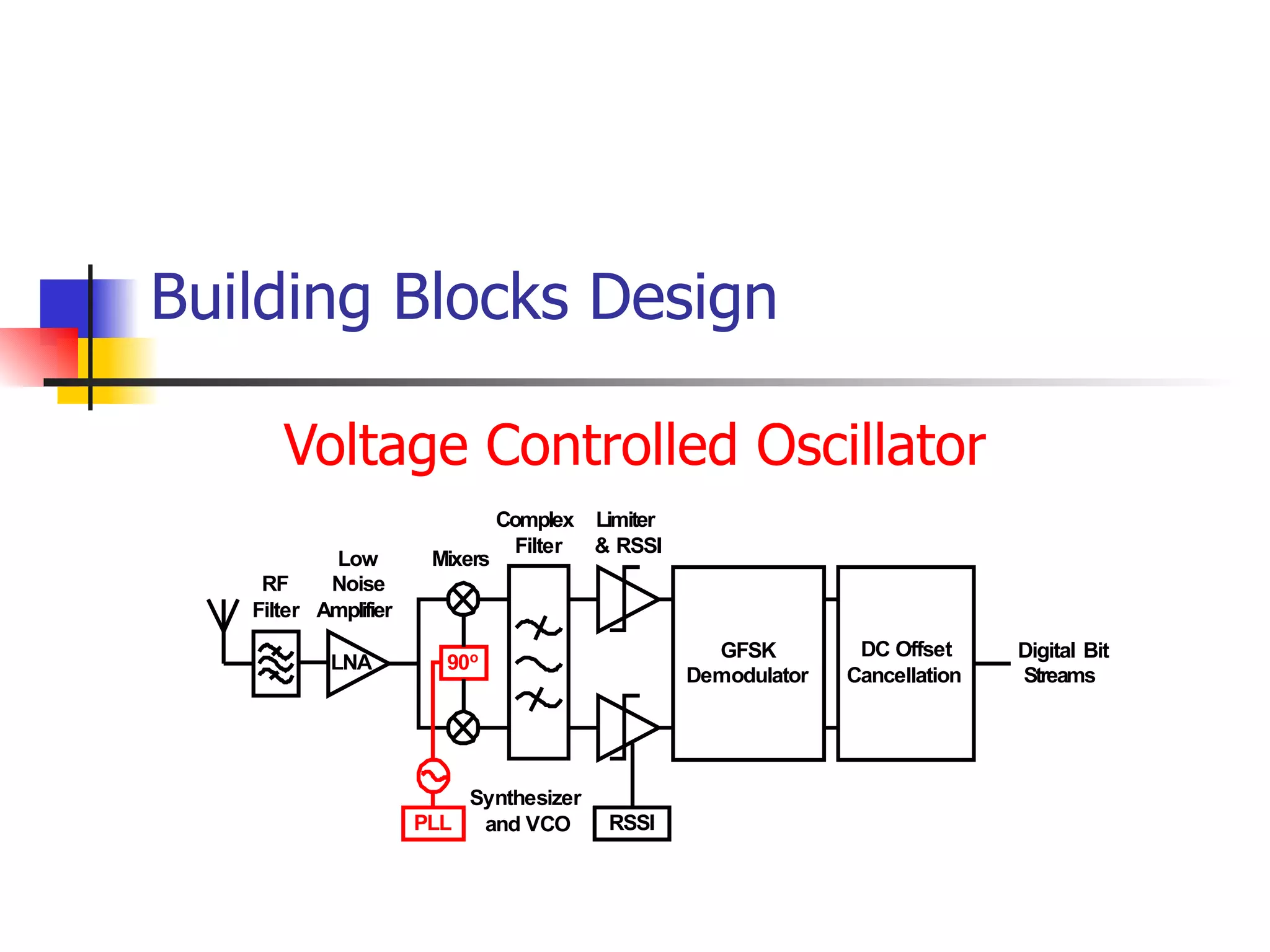
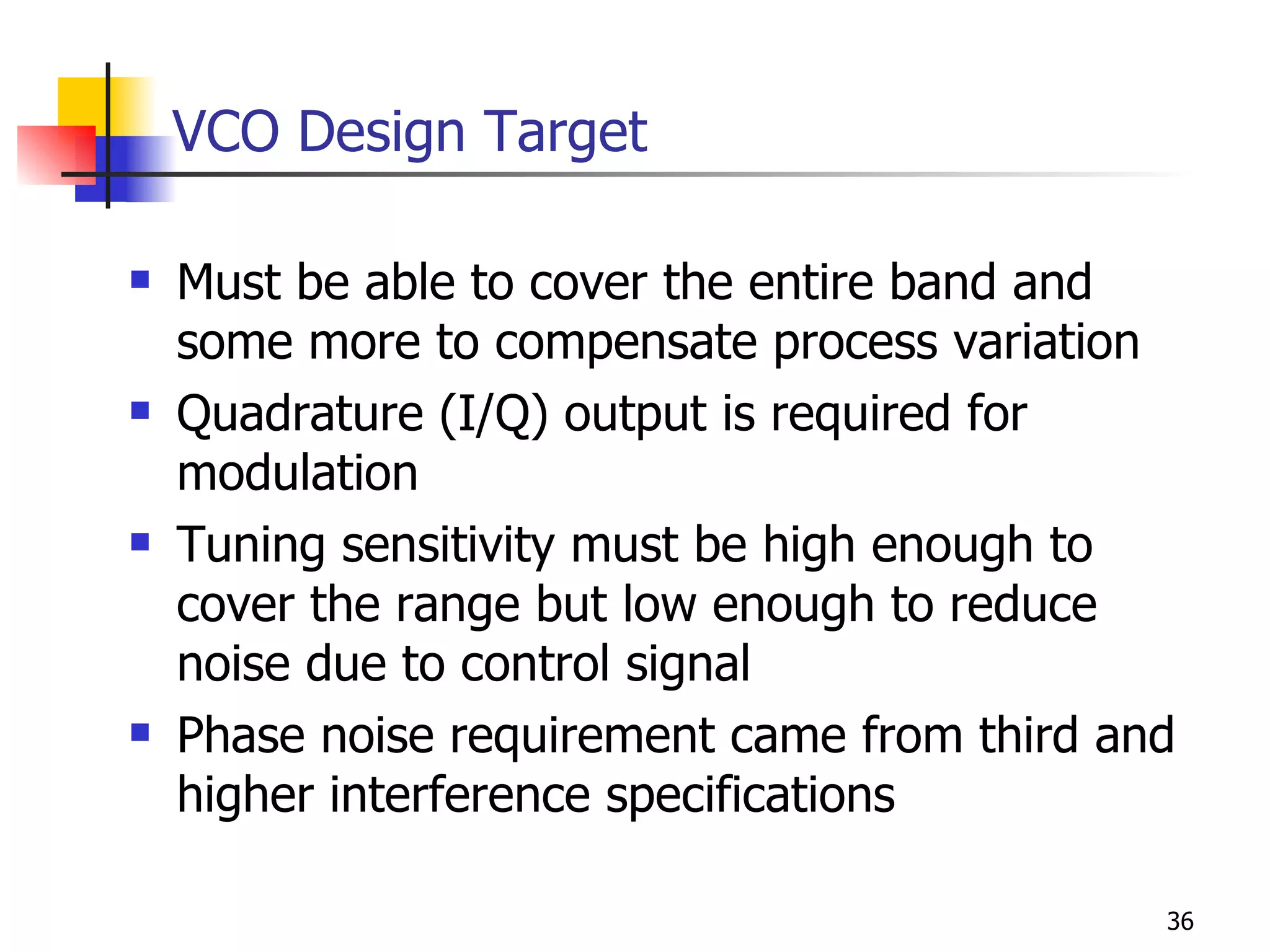
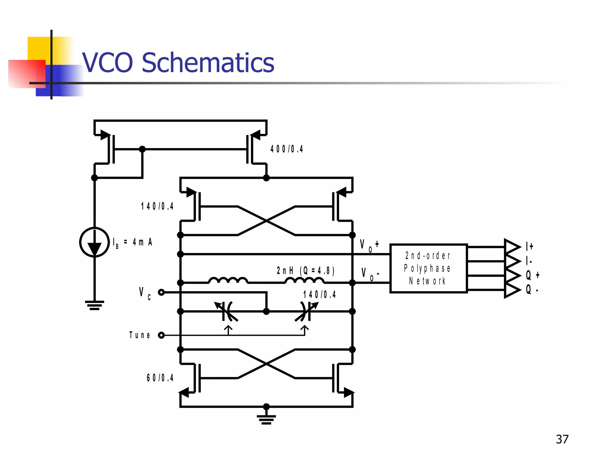
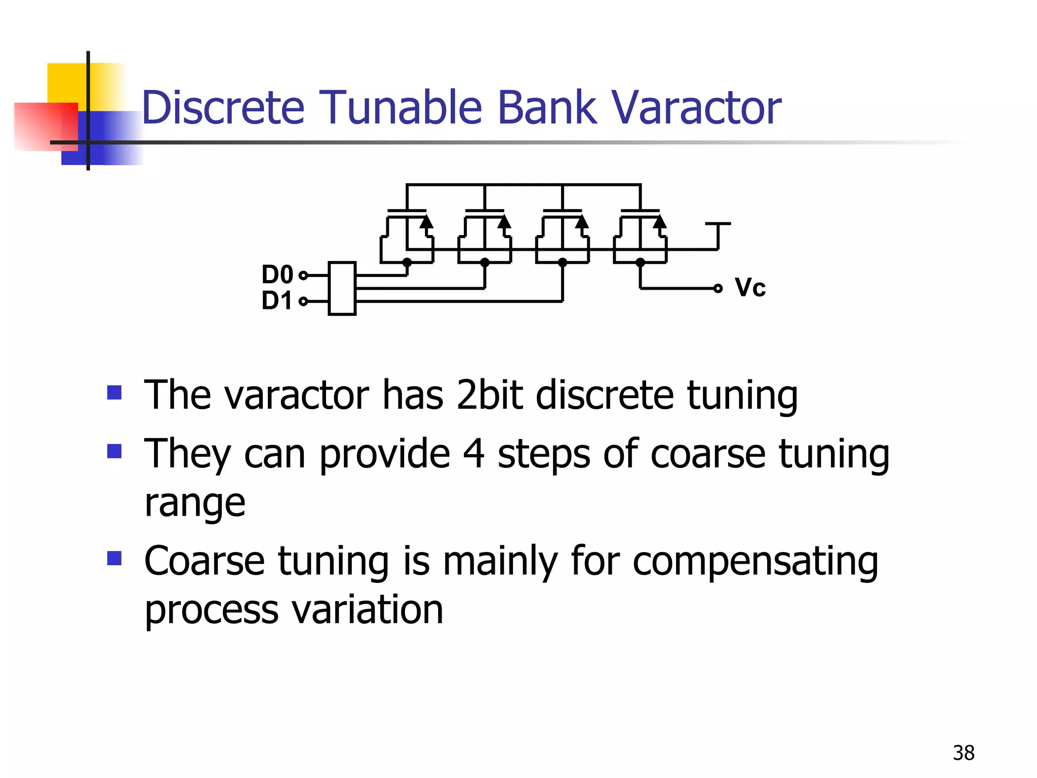
Development of VCOs including design targets and schematics for performance enhancement across frequencies.
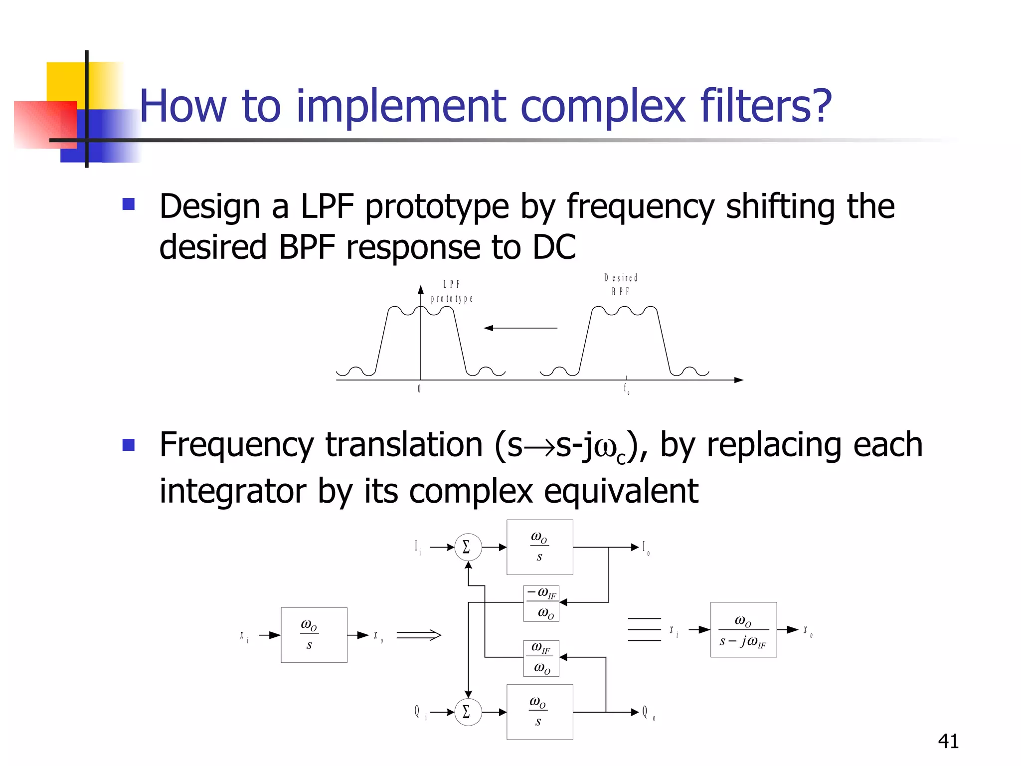
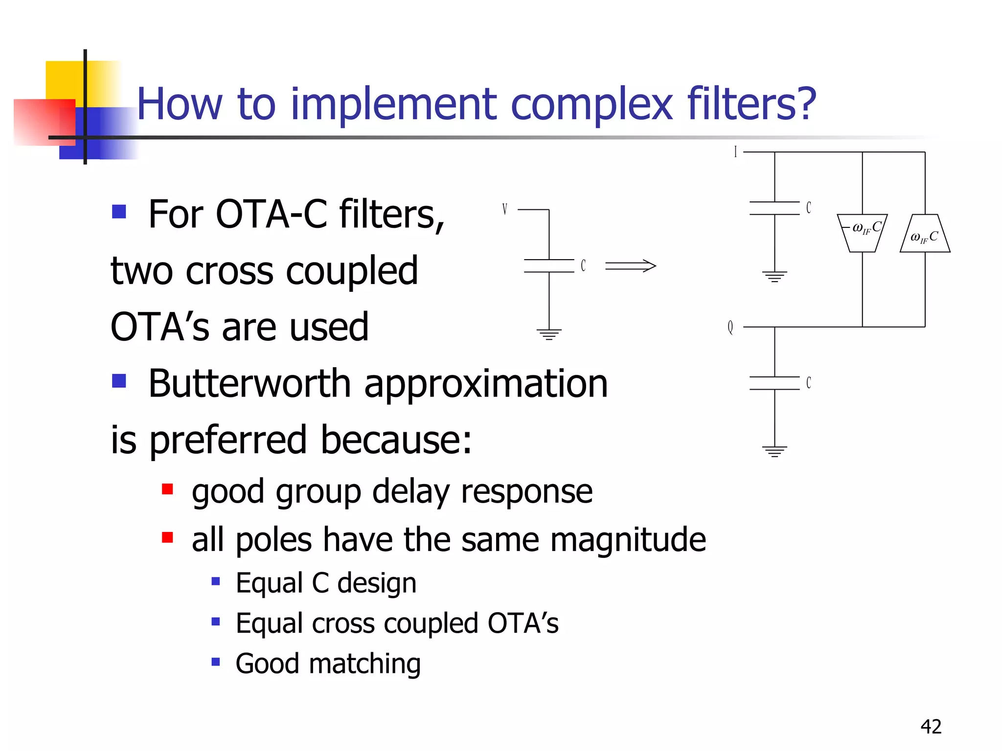
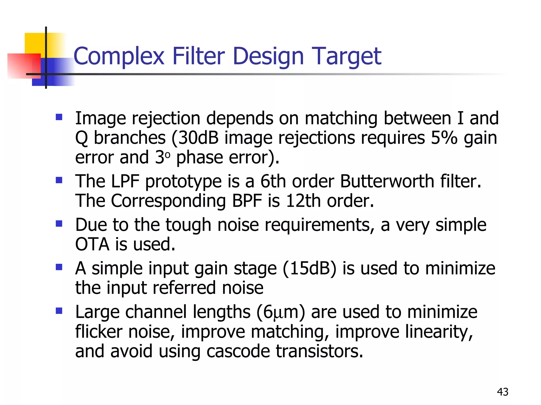
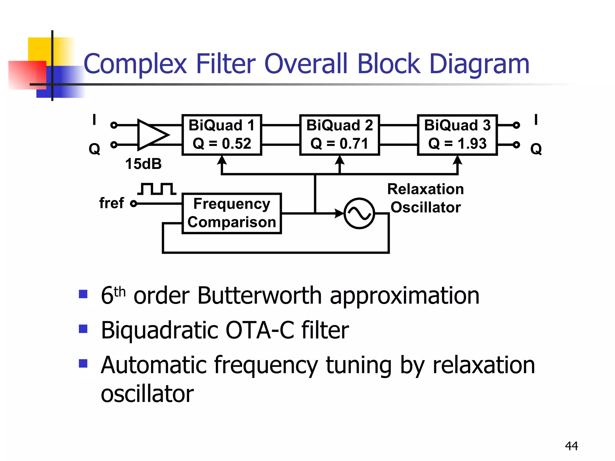
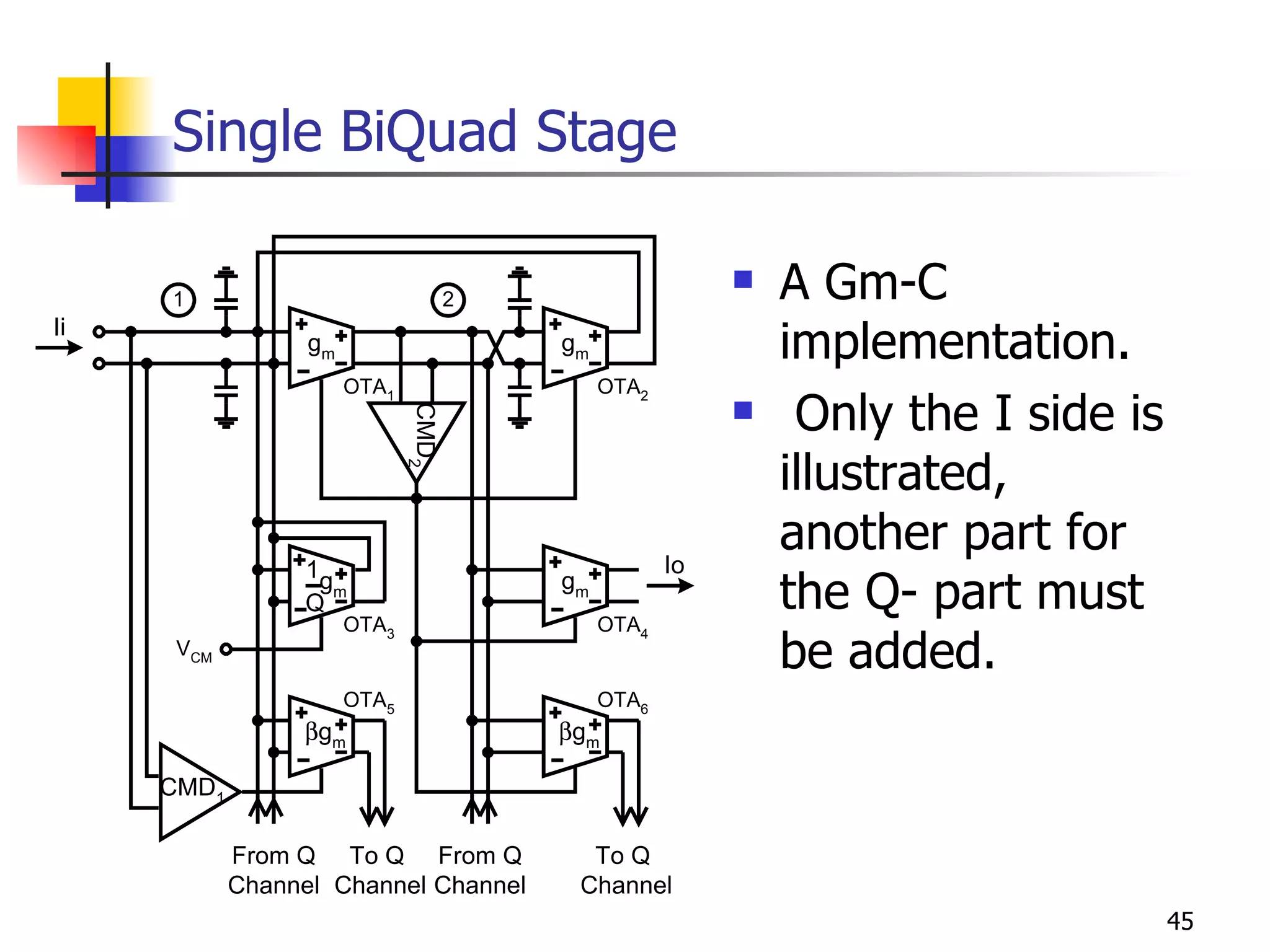
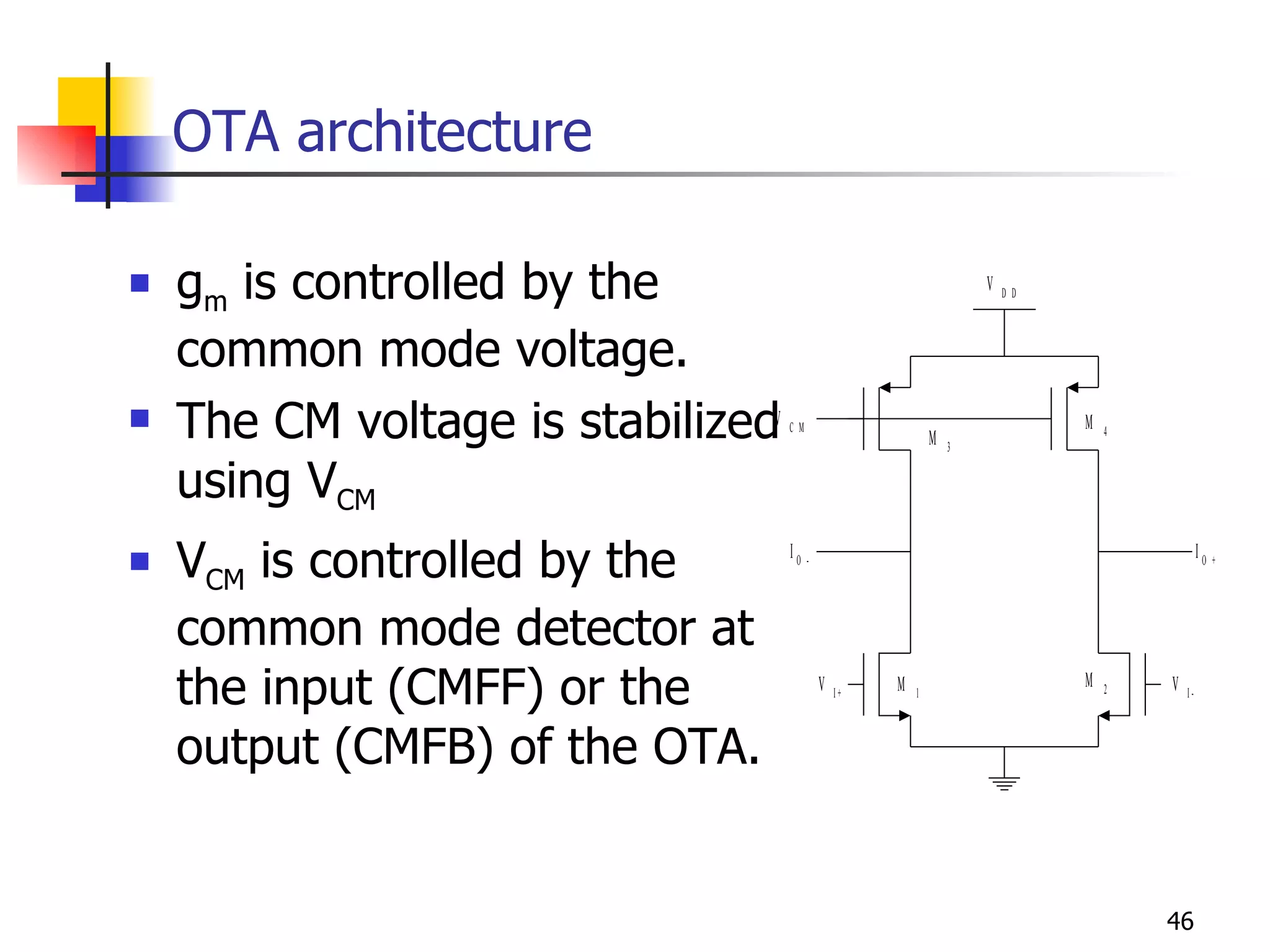
Detailed methods on implementing complex filters, focusing on image rejection, attenuation, and performance metrics.
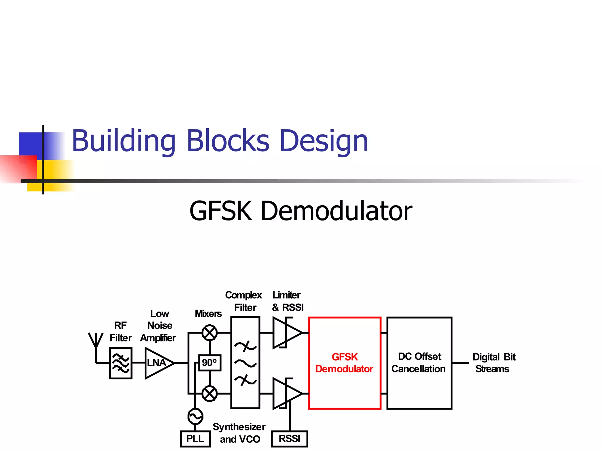
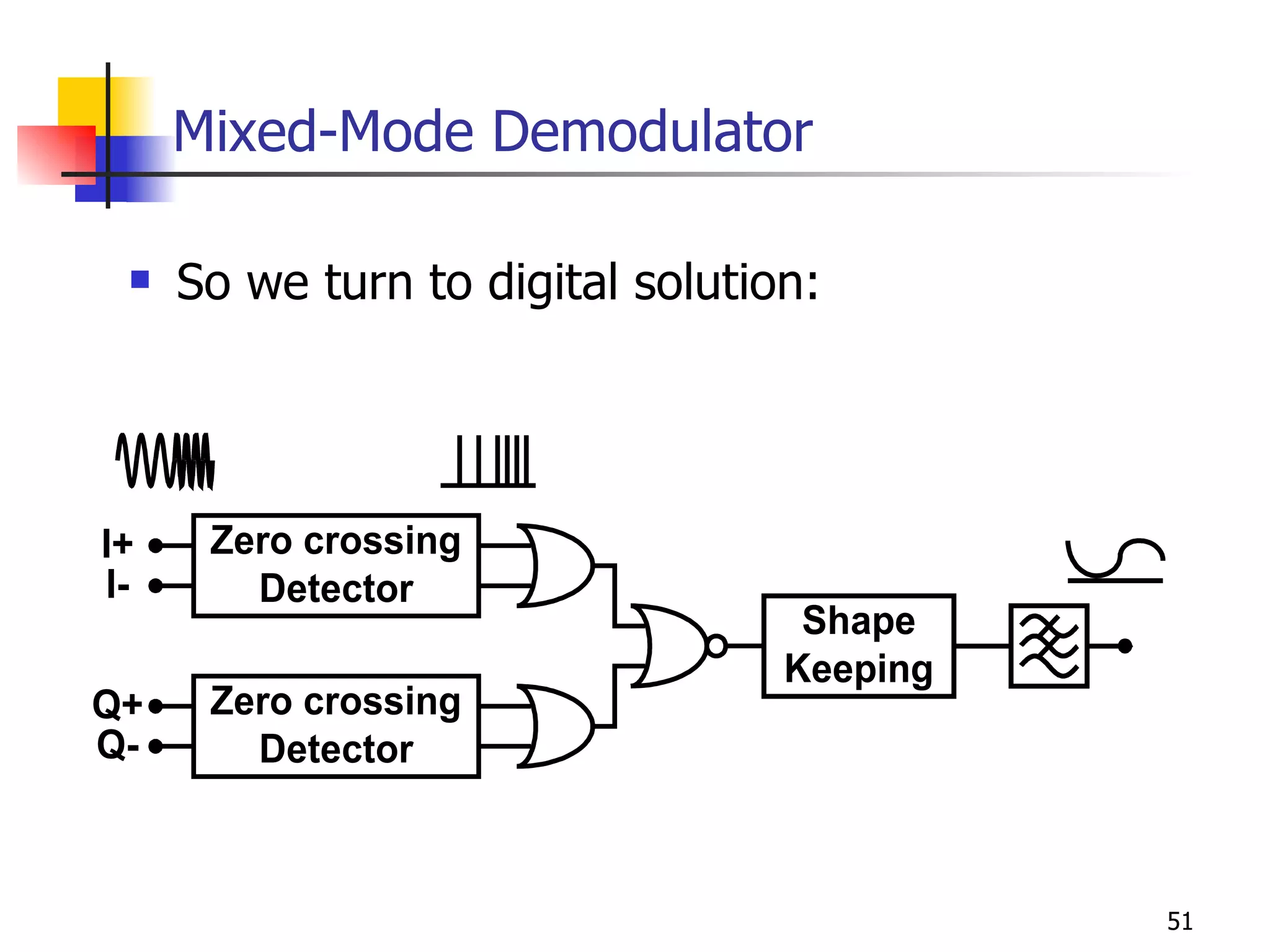
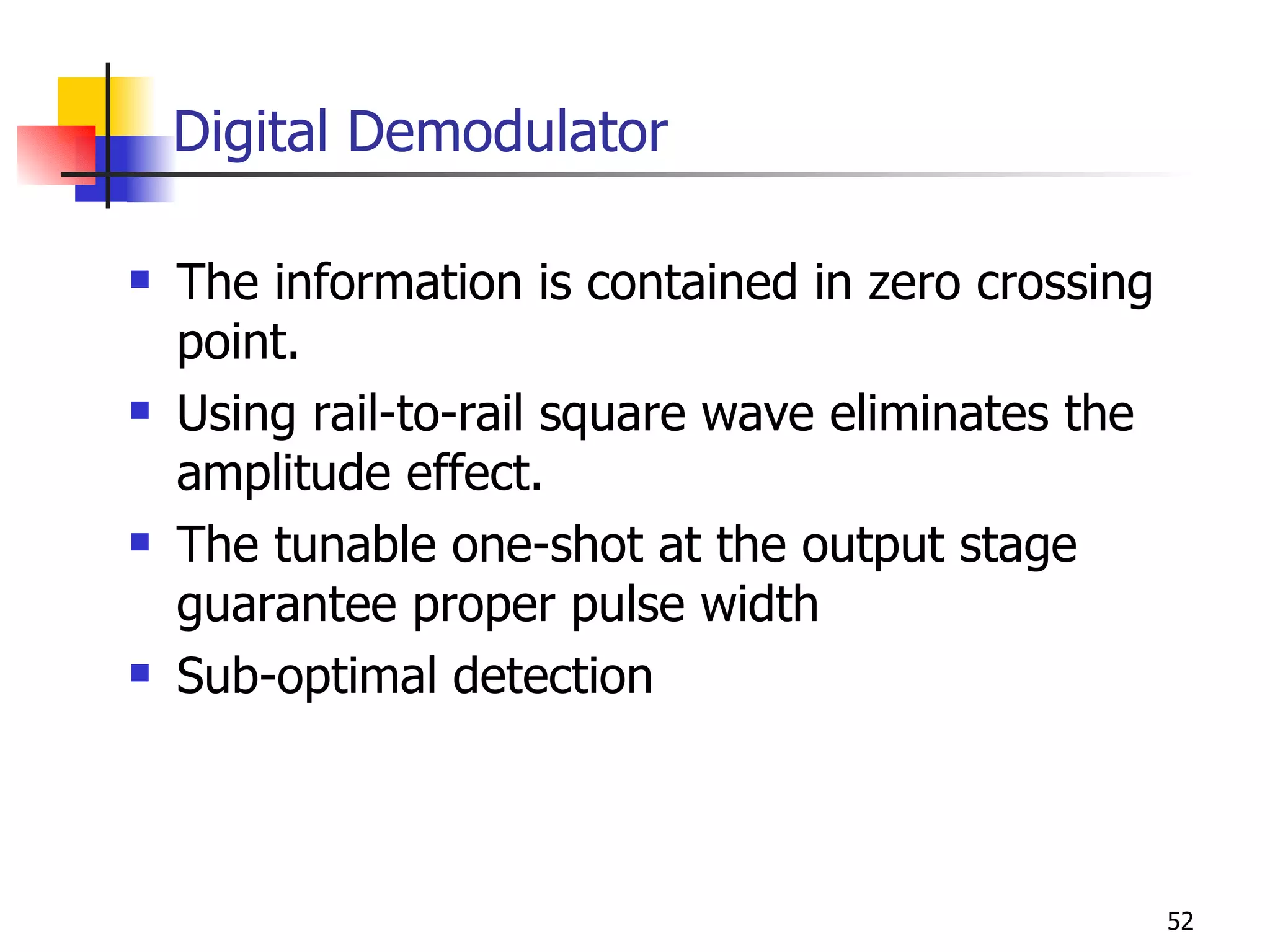
Designing a mixed-mode GFSK demodulator, highlighting motivations and digital solutions for power efficiency.
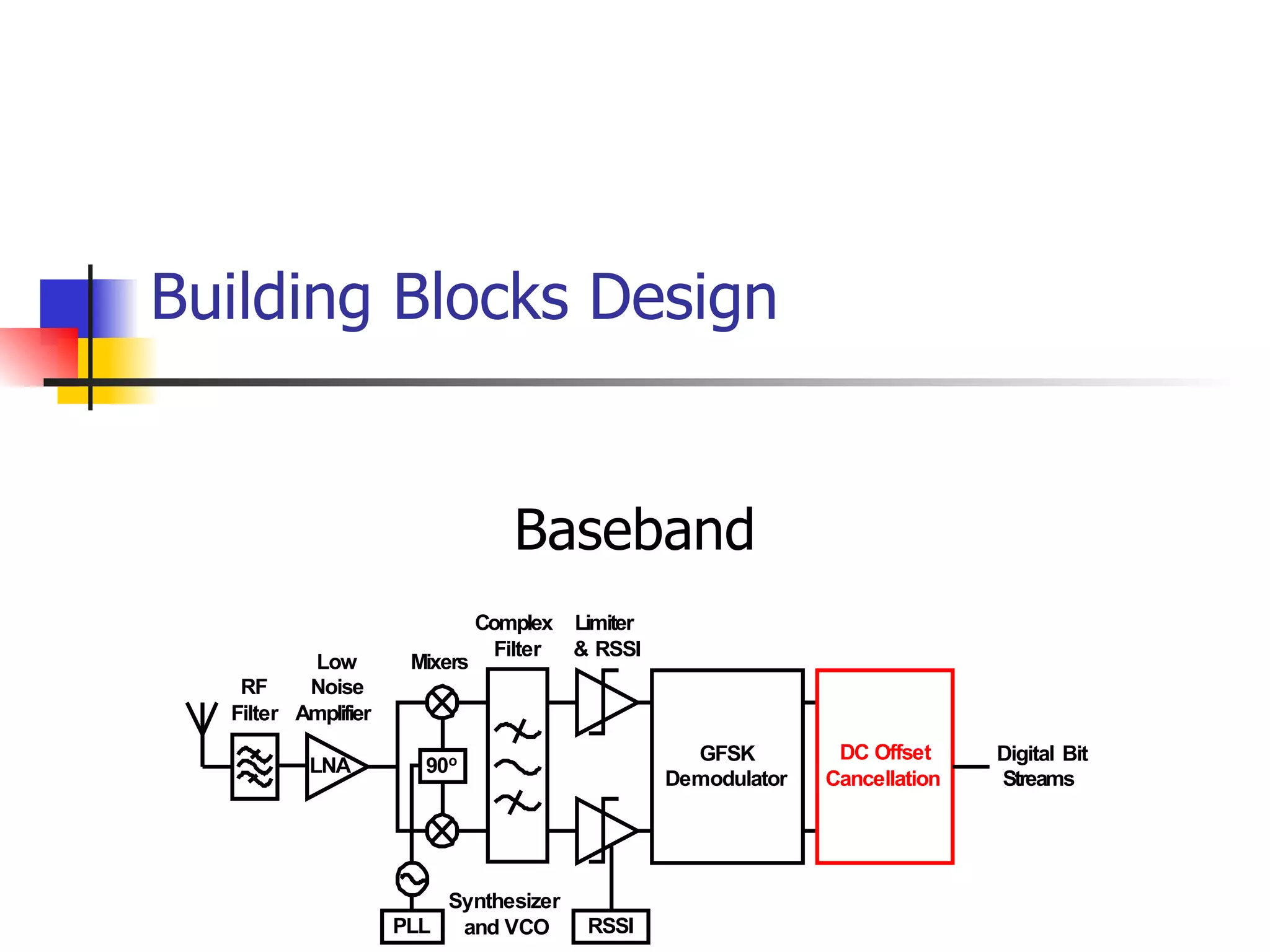
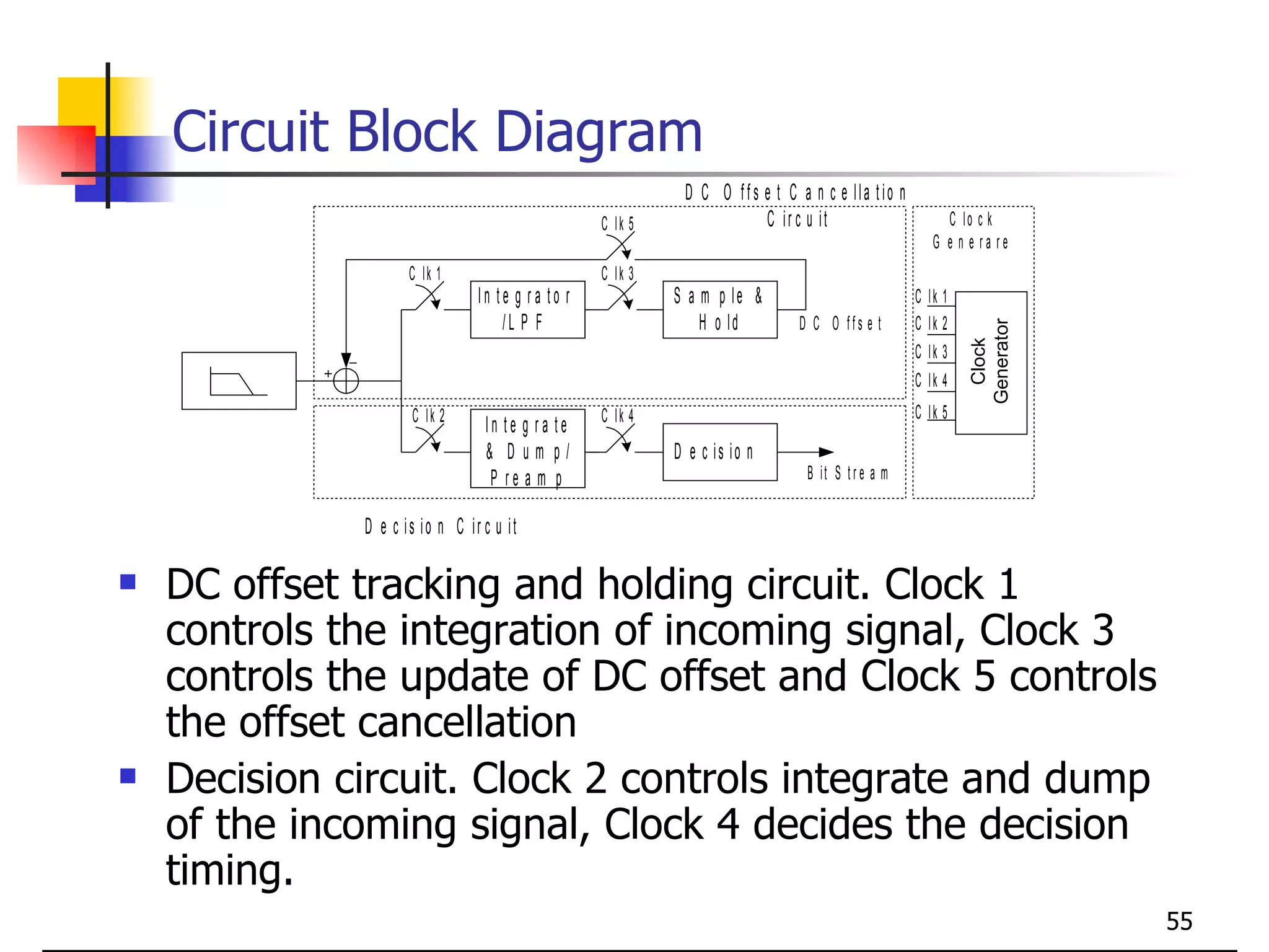
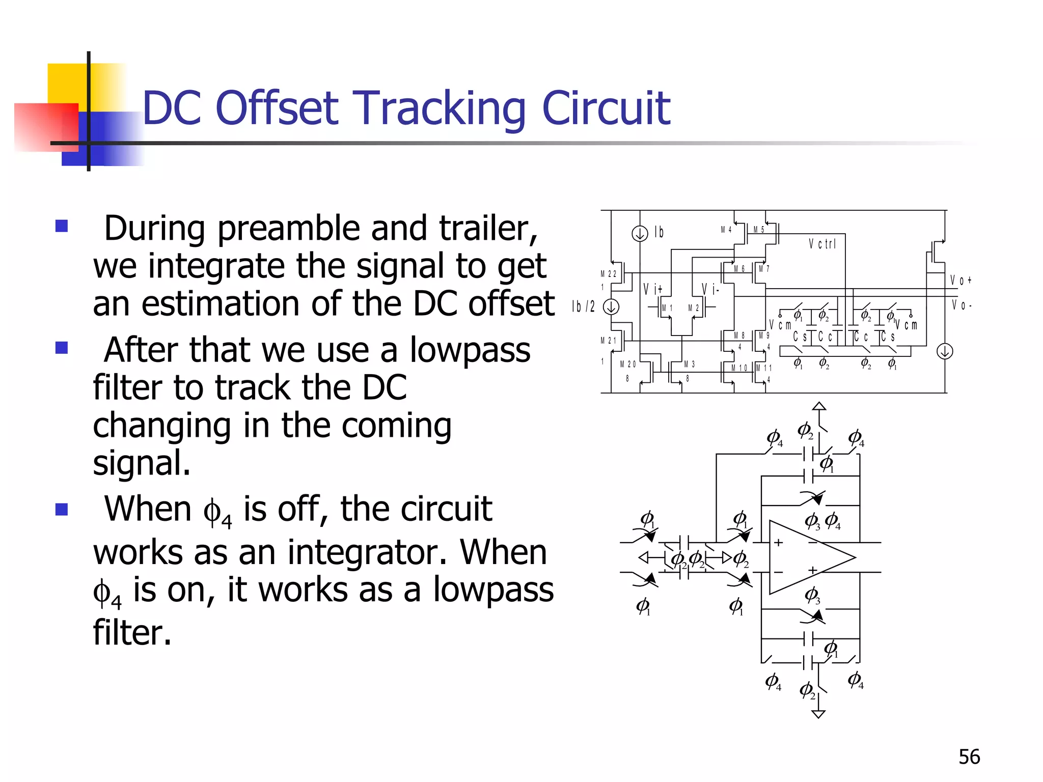
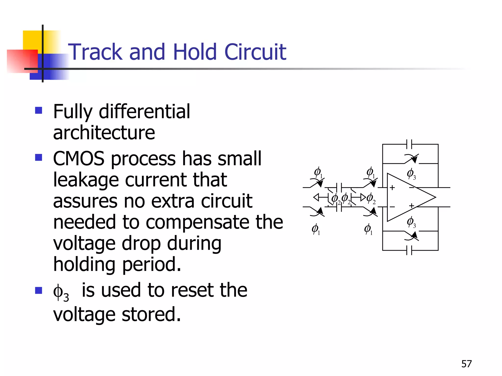
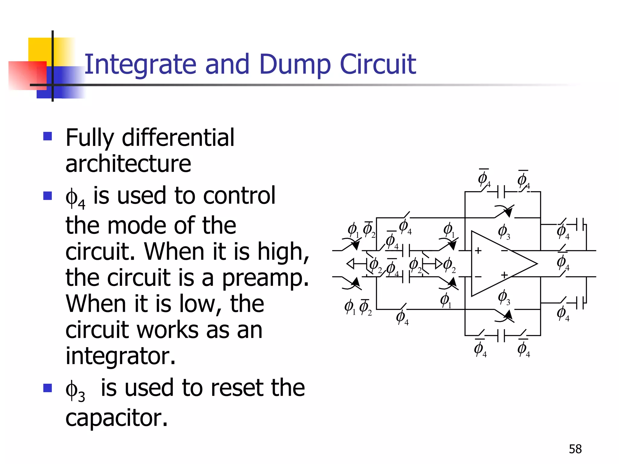
Overview of baseband circuit functionalities including bit decision, DC offset tracking, and control signal generation.
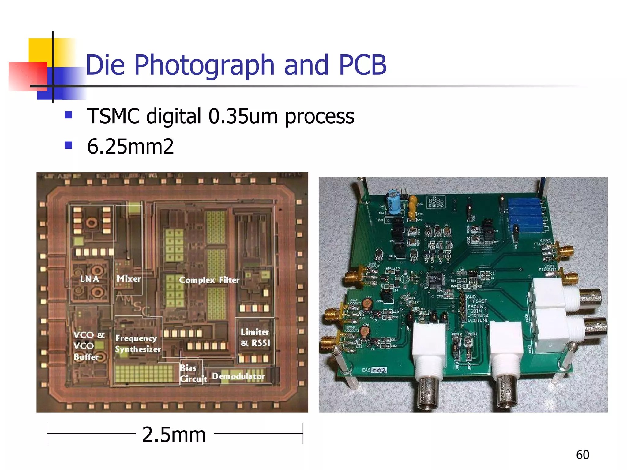
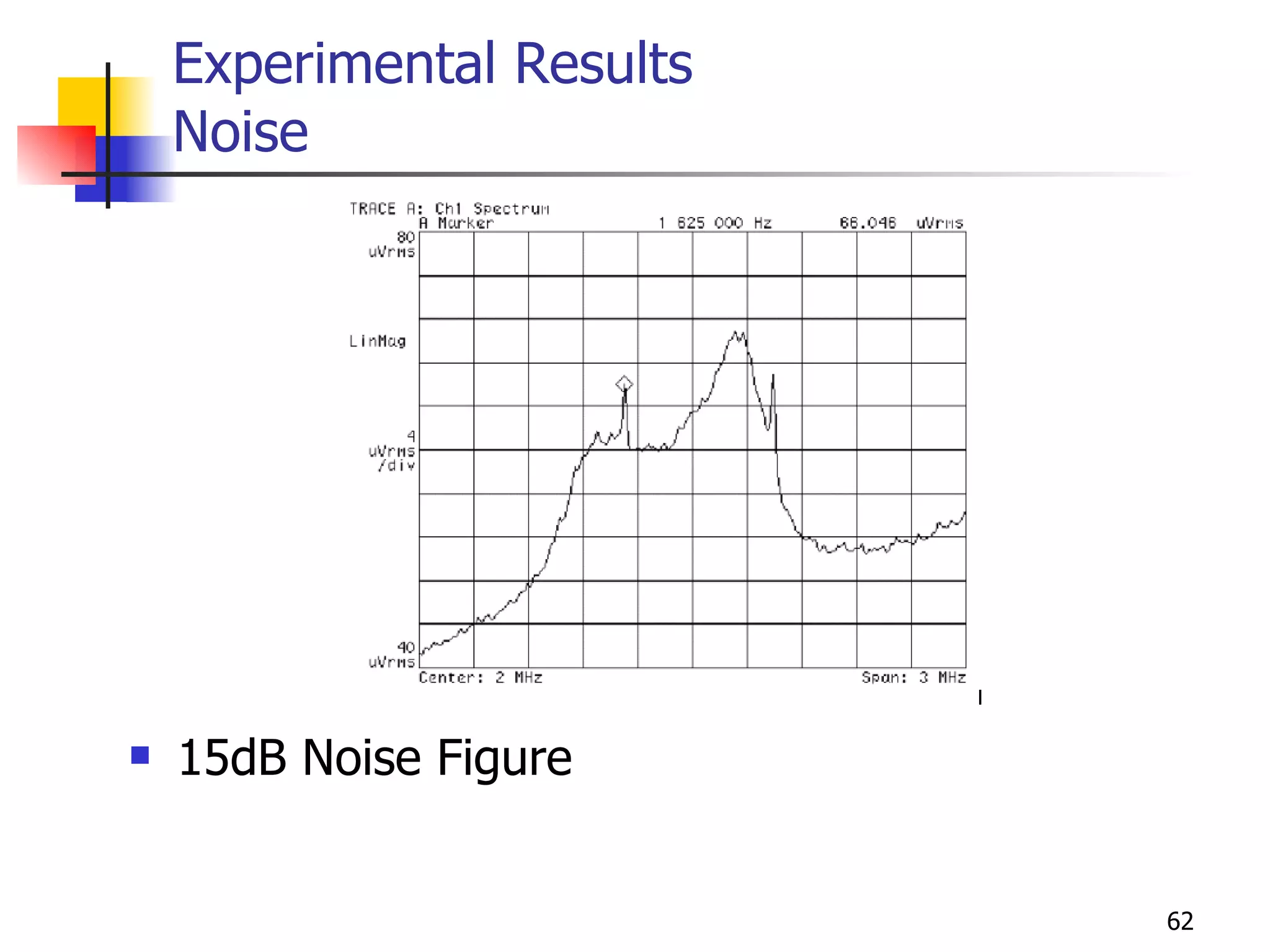
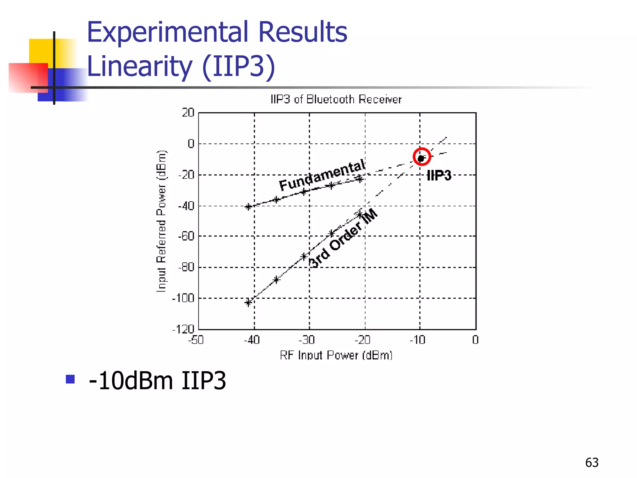
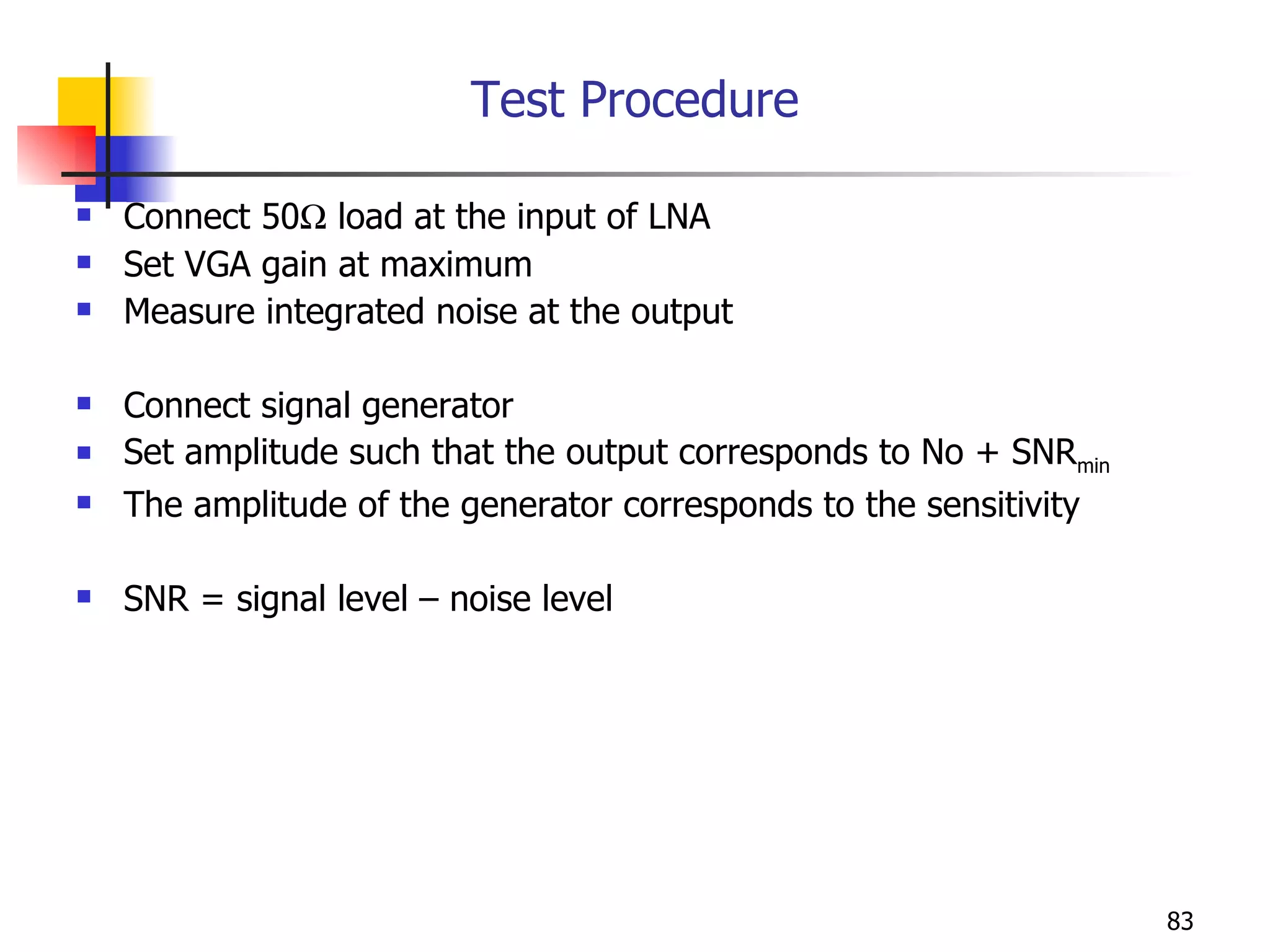
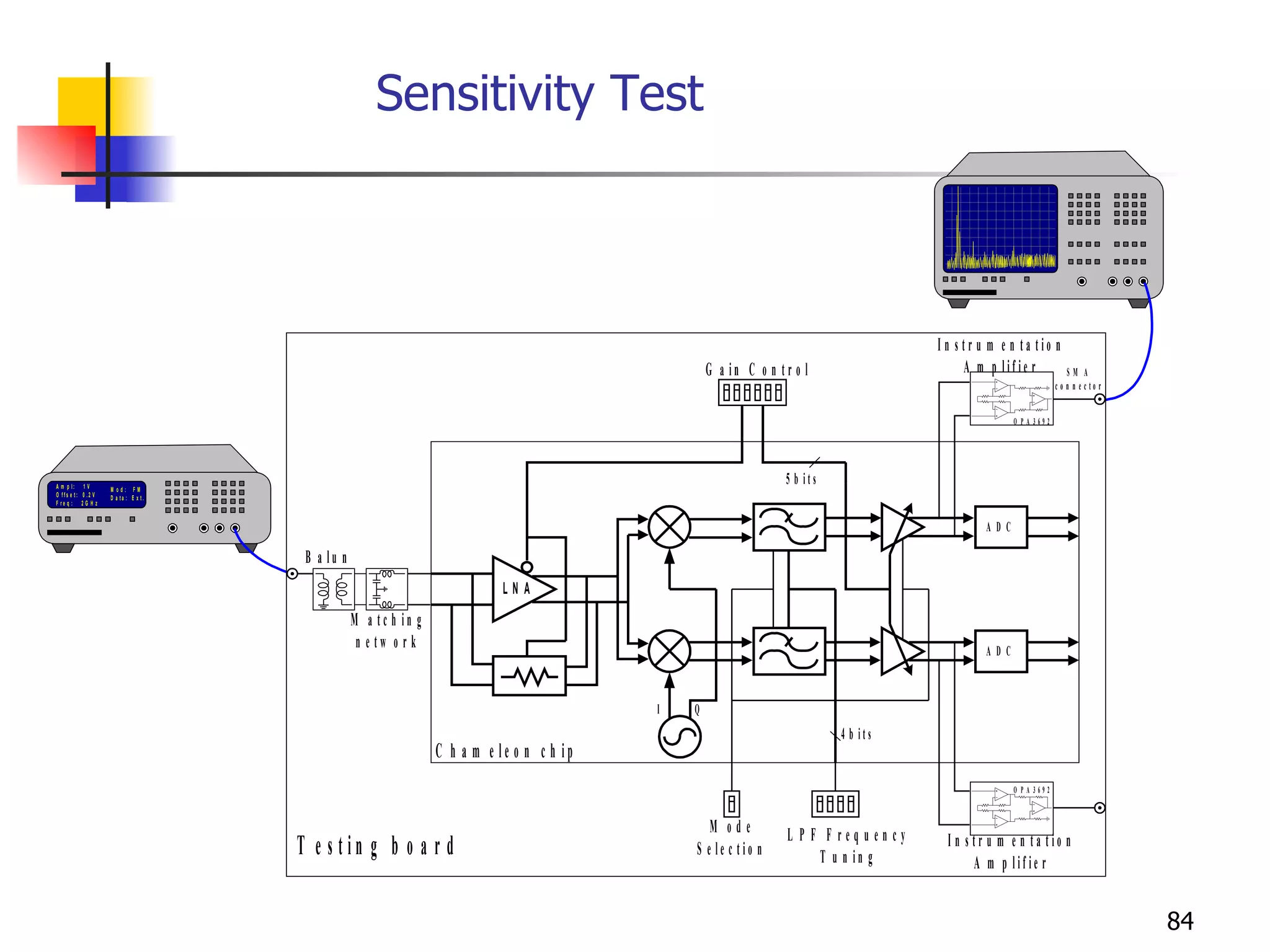
System testing results showcasing sensitivity, noise figures, and performance specifications of the Bluetooth receiver.
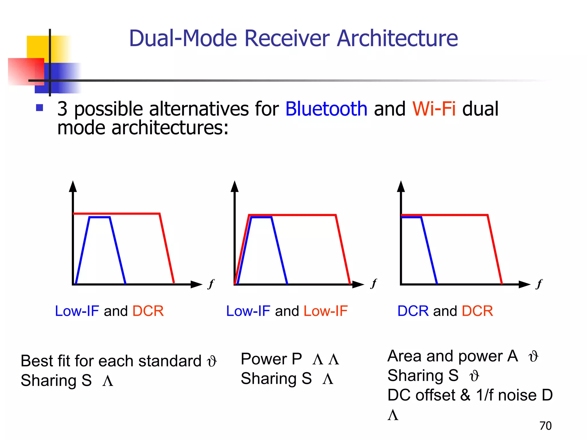
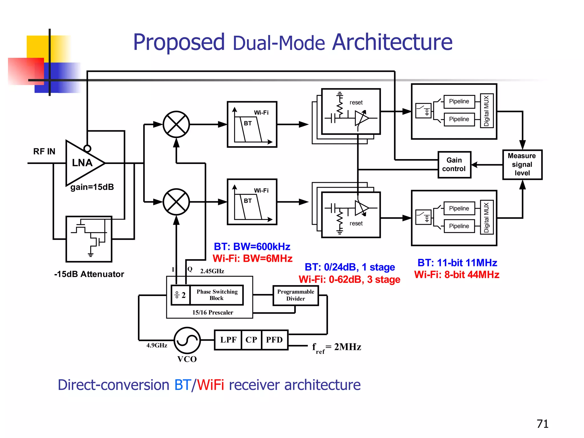
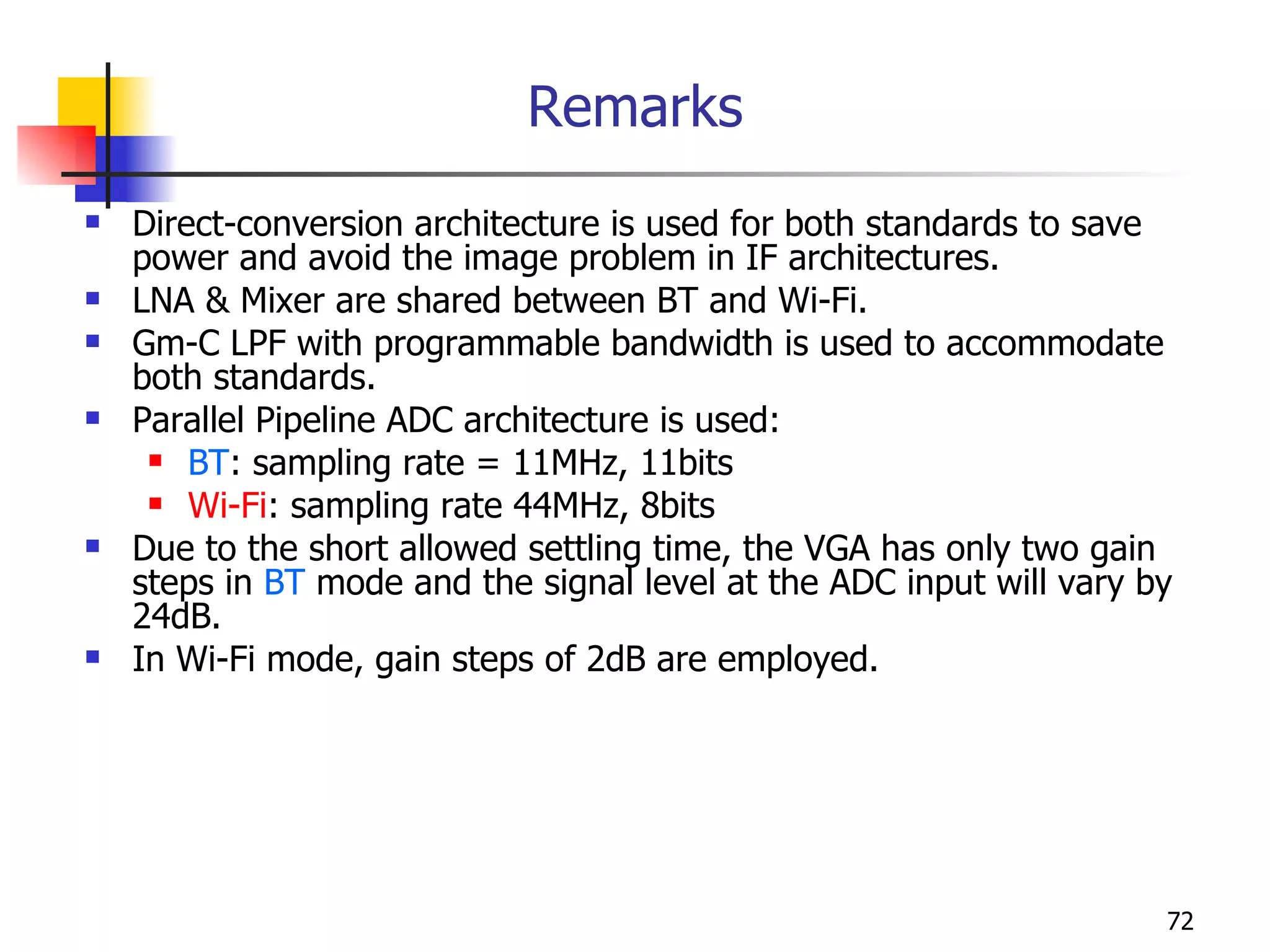
Design implications for a dual-mode transceiver accommodating Bluetooth and Wi-Fi standards, emphasizing integration.
Architecture proposal for dual-mode receiver focusing on power saving, sharing components, and specifications.
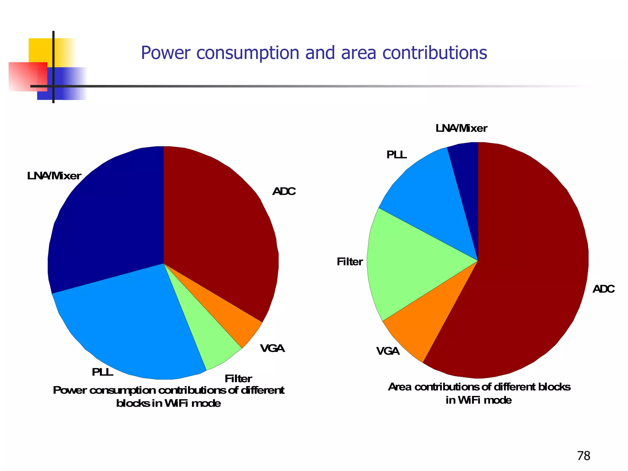
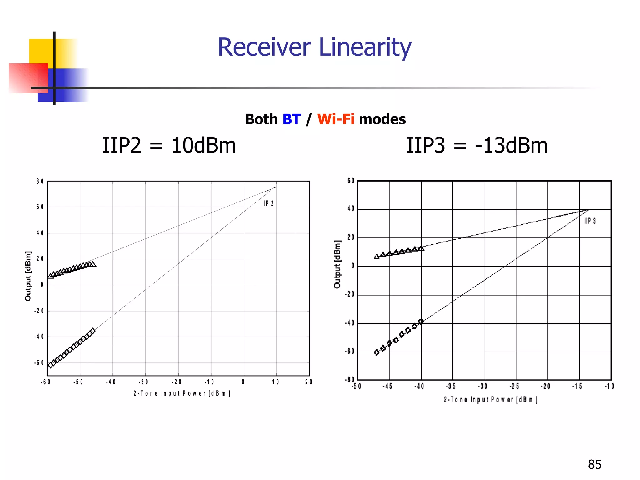
Overview of design contributions for noise figure, IIP3, area, and power consumption in the dual-mode architecture.
Summary of the Chameleon receiver prototype's achievements in efficiency, integration, and design implications.
Acknowledgments of collaborative contributions and a list of technical references used in the design.


![RF Module Design - [Chapter 4] Transceiver Architecture](https://cdn.slidesharecdn.com/ss_thumbnails/rfch4-150613070346-lva1-app6891-thumbnail.jpg?width=640&height=640&fit=bounds)


![Multiband Transceivers - [Chapter 6] Multi-mode and Multi-band Transceivers](https://cdn.slidesharecdn.com/ss_thumbnails/ch6-150613070935-lva1-app6891-thumbnail.jpg?width=640&height=640&fit=bounds)


