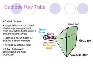
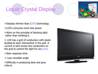
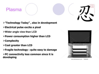
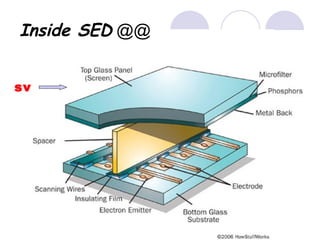
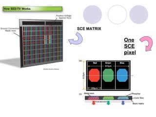
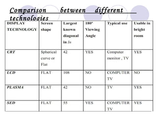
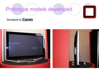
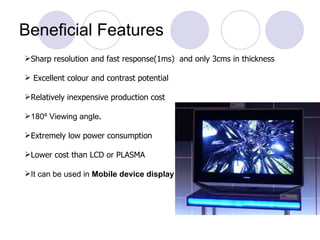
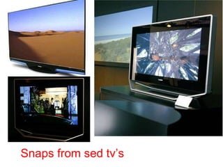
SEMINAR   on SED A d a r s h  .S
COMMON DISPLAY TECHNOLOGIES  :   AN OVERVIEW
Cathode Ray Tube Earliest displays A specialized vacuum tube in which images are produced when an electron beam strikes a phosphorescent surface  Later  RGB  colour model for displays in colour monitors Affected by external fields Bulky , high power consumption and heat production
Liquid Crystal Display Displays thinner than ( CRT ) technology.  LCD’s consume much less power  Work on the principle of blocking light  rather than emitting it.  LCD has a grid of conductors with pixels located at each intersection in the grid. A current is sent across two conductors on the grid to control the light for any  pixel .  Slow response time Less viewable angle Difficulty in producing dark and grey colours
Plasma ” Technology Today” , also in development Electrical pulse excite a pixel Wider angle view than LCD Power consumption higher than LCD Complexity Cost greater than LCD Fragile technology : quite easy to damage PC connectivity less common since it is  developing
Buzz into   SED ?? Wider angle view  !!!! Lower cost  !!!! Superior picture quality  !!!! Less complexity in overall terms  !!!!
“  SURFACE  CONDUCTION ELECTRON  EMITTER  DISPLAY ” Combine CRT  into  LCD technology. Millions  of miniature CRTs, called surface-conduction electron emitters (SCEs) embedded in surface. “ High quality picture in low centimeter thickness” Only 3cm thickness
Inside SED  @@ sv
how SED works  ?? An SED-TV has millions of these SCE s arranged in a  matrix  , and each one  controls the Red, Green or Blue aspect of one pixel of the picture. Rather than  directing electrons to create the image one row at a time, the matrix activates all the  SCE s needed to create the picture virtually simultaneously
SCE MATRIX One SCE pixel One SCE pixel
In short ……............ ……………… tied together When the SED-TV receives a signal,, a) Scans the signal  b) Decides what to do with the red, green and blue aspect of each pixel  c) Activates the necessary SCE s, which generate electrons that fly through the vacuum to the screen
Comparison  between  different  technologies
Prototype models developed Developed by  Canon
Beneficial Features Sharp resolution and fast response(1ms)  and only 3cms in thickness Excellent colour and contrast potential  Relatively inexpensive production cost 180º Viewing angle .   Extremely low power consumption Lower cost than LCD or PLASMA  It can be used in  Mobile device display
Snaps from sed tv’s
Challenges Unknown (though optimistic) life expectancy  Potential for screen burn-in : but expected to overcome  due to phosphor development Currently prototype only  expected soon
References: Document-United States Patent 7548017  engadgetHD Nanotechnology, Transactions on Volume 7, Issue 4, July 2008.  Audioholics www.cnet.com www.newtechnologyworld.com
By  A d a r s h
Questions

Surface Conduction Electron Emitter Display

  • 1.
    SEMINAR on SED A d a r s h .S
  • 2.
  • 3.
    Cathode Ray TubeEarliest displays A specialized vacuum tube in which images are produced when an electron beam strikes a phosphorescent surface Later RGB colour model for displays in colour monitors Affected by external fields Bulky , high power consumption and heat production
  • 4.
    Liquid Crystal DisplayDisplays thinner than ( CRT ) technology. LCD’s consume much less power Work on the principle of blocking light rather than emitting it. LCD has a grid of conductors with pixels located at each intersection in the grid. A current is sent across two conductors on the grid to control the light for any pixel . Slow response time Less viewable angle Difficulty in producing dark and grey colours
  • 5.
    Plasma ” TechnologyToday” , also in development Electrical pulse excite a pixel Wider angle view than LCD Power consumption higher than LCD Complexity Cost greater than LCD Fragile technology : quite easy to damage PC connectivity less common since it is developing
  • 6.
    Buzz into SED ?? Wider angle view !!!! Lower cost !!!! Superior picture quality !!!! Less complexity in overall terms !!!!
  • 7.
    “ SURFACE CONDUCTION ELECTRON EMITTER DISPLAY ” Combine CRT into LCD technology. Millions of miniature CRTs, called surface-conduction electron emitters (SCEs) embedded in surface. “ High quality picture in low centimeter thickness” Only 3cm thickness
  • 8.
  • 9.
    how SED works ?? An SED-TV has millions of these SCE s arranged in a matrix , and each one controls the Red, Green or Blue aspect of one pixel of the picture. Rather than directing electrons to create the image one row at a time, the matrix activates all the SCE s needed to create the picture virtually simultaneously
  • 10.
    SCE MATRIX OneSCE pixel One SCE pixel
  • 11.
    In short ……............……………… tied together When the SED-TV receives a signal,, a) Scans the signal b) Decides what to do with the red, green and blue aspect of each pixel c) Activates the necessary SCE s, which generate electrons that fly through the vacuum to the screen
  • 12.
    Comparison between different technologies
  • 13.
    Prototype models developedDeveloped by Canon
  • 14.
    Beneficial Features Sharpresolution and fast response(1ms) and only 3cms in thickness Excellent colour and contrast potential Relatively inexpensive production cost 180º Viewing angle . Extremely low power consumption Lower cost than LCD or PLASMA It can be used in Mobile device display
  • 15.
  • 16.
    Challenges Unknown (thoughoptimistic) life expectancy Potential for screen burn-in : but expected to overcome due to phosphor development Currently prototype only expected soon
  • 17.
    References: Document-United StatesPatent 7548017 engadgetHD Nanotechnology, Transactions on Volume 7, Issue 4, July 2008. Audioholics www.cnet.com www.newtechnologyworld.com
  • 18.
    By Ad a r s h
  • 19.