This document describes a method for fabricating both negative and positive patterns on a single layer of positive photoresist. The method involves locally crosslinking the photoresist using laser exposure, followed by a flood UV exposure and development. The crosslinked areas form a negative pattern, while the non-exposed areas form a positive pattern. Experimental results showed that the height of the negative pattern can be controlled by varying the laser exposure energy and other processing parameters.
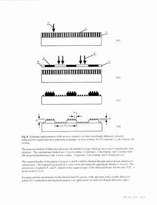
![a) The substrate ( I) with a metal layer (2) is coated with positive pliotoresist (3
h The laser beam (4) exposes photoresist locally in accordance with the negative (5) and positive (6)
pattern structures.
c) The photoresist layer is exposed with IJV light (7> through a pholomask (8 . The photomask has
transparent (9) and opaque (10) areas which correspond to the negative (5) and posItive(6) type pattern areas
needed.
After development of the photoresist layer, negative ( I I) and positive (12) pliotoresist patterns arc
created in resist on the metal surface.
The patterns are etched into the metal layer. The negative (13) and positive ) 14) type metal patterns are
created on the substrate surface.
Standard glass plates. I 'x 1" to 5" x 5" in site were used. The substrates were cleaned and dehydration
baked. Next the substrates were spin coated with positive photoresist. Different layer thicknesses were
applied by varying the spin speed and resist viscosity. In the current RP(' laserwriting system. a helium-cadmium
laser operating at 441 nm is used to expose the resist coated substrate, which is niounted on an
r-O air hearing spindle. Machine hardware and environment are sublect to closed-loop control to maintain
feature placement accuracy in the PPfl1 range. A 0.7pin laser beam spot site was used and the exposure
energ varied from 0.05 J/cm to 2.4 J/cm. Theexposure energy at fects the width of the exposed area as
well as the height of the negative photoresist pattern on the substrate. For experimental parts the
laserwriter was programmed to write a (qtni wide ring every S0pni.
The parts covered by chrome and gold layers were etched in chromium and gold etch solutions, respectively.
Results were obtained using optical profilometrv Zygo New View white-light surface profilomctem1 and
optical microscopy (Nomarski microscope).
3. RESULTS AND DISCUSSION
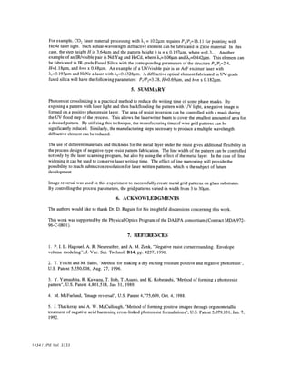
Figure 2 shows the results of an experimental part. The trenches on the positive pattern (bottom of the
picture) become the rectangular steps on the negative pattern (top of the picture. The top halt of the
pattern I Fig. 2h)] is the portion where the crosslinked resist behaves like a negative pattern The bottom
half of the pattern Fig. 2(c )I was masked during the UV flood exposure. The laser written pattern on this
part of the sample behaves like positive tone resist.
Fig. 2(a) Optical profilomctrv data of an experimental part.
(428 .SP)L t'oI. 3333](https://image.slidesharecdn.com/8a5b6b92-6bf3-4ef4-ba22-4400c132a4ee-141130135754-conversion-gate01/85/SPIE-Vol-3333-3-320.jpg)
![The height of the negative pattern is O.7311m [Fig. 2(h)], while the depth of the positive pattern is I
[Fig. 2(c)]. This gives a ratio of 1:2.7 for the negative to positive step tahncatcd by the laser beam
crosslinking method. This ratio can he controlled by varying the parameters of the process. e.g. the laser
exposure energy. the intermediate hake temperature and duration, and the UV 1100(1 exposure energy. The
intersect region between the positive and negative pattern areas can he inininiiied by providing a vacuum
contact between the mask and substrate during the UV flood exposure step. Various resist thicknesses.
writing parameters. intermediate hake parameters. flood exposure dosages. and developriient times were used
for process optimization. Because the height of the negative resist pattern that can be obtained with this
method is typically only a fraction (1/2 to 1/3) ot the initial resist layer thickness, it is difficult to control
the exposure and development parameters required to produce resist layers that are less than lllin in
thickness. On the other hand, for resist layers greater than 5pm in thickness, it is difficult to clear the flood
exposed areas completely because of resist hardening during the intermediate hake. A resist thickness of 3
to 511m is optimal for the reliable fabrication of the negative-type resist patterns.
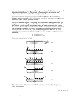
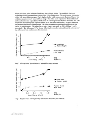
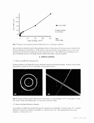
The results in Fig. 3 show how laser power affects the negative pattern height and line width. For the
range of laser energies investigated, the height changed by ôO'3 and line width by 7ft/ . Further
investigations showed that this effect is stronger when the resist layer is spun on a metal-coated substrate.
Fig. 4 displays the results of such dependence for the same type of resist as in Fig. 3. hut spun on a
substrate coated with a 200 nm thick cold layer. The gold layer causes approximately a 5 times larger
iii i.
)ptical profilometry data of the UV flood exposed area (negative-type pattern.
Fig. 2(c) Optical profilometrv data of the unexposed UV flood exposure area positi'e-type pattern).](https://image.slidesharecdn.com/8a5b6b92-6bf3-4ef4-ba22-4400c132a4ee-141130135754-conversion-gate01/85/SPIE-Vol-3333-4-320.jpg)
![I I I I I I
(a)
I Ii fl fl fl fl fl rir n n n n nfl n n n n nfl n n n n ii n
_____________________________________I
ptInntl poonci panuq
ru Innnnnl Innnnnl Ii,
(c)
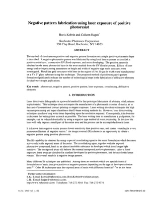
Fig. 7 Schematic representation of diffractive optical elements (DOEs): a) DOE for relatively long
wavelength; b) DOE for relatively short wavelength; c) dual-wavelength DOE.
The conventional method of fabrication for such elements consists of two lithography steps with an
alignment process in-between, and two etching processes:
First cycle:
1 . The substrate is coated with a resist layer and softbaked.
2. The resist layer is exposed through the first photomask, corresponding to pattern P2
3. The resist layer is developed in developer solution and hardbaked.
4. The substrate is etched by either a wet or dry etching process.
5. The resist is stripped from the surface of the substrate.
Second cycle:
6. The substrate is coated with a resist layer and softbaked.
7. The resist layer is exposed through the first photomask, corresponding to pattern P1.
8. The resist layer is developed in developer solution and hardbaked.
9. The substrate is etched in a wet or dry etching process.
10. The resist is stripped from the surface of the substrate.
Using the proposed method of positive/negative pattern fabrication on a single resist layer, the dual-wavelength
diffractive element can be manufactured by following this sequence of steps (Fig. 8):
1. The substrate is coated with a resist layer and softbaked.
2. The resist layer (1) is exposed with a laser beam (2) which creates the pattern (3) corresponding
to period P2 [Fig. 8(a)].
3. The resist layer is baked.
4. The resist layer is exposed by UV light (4) through a photomask (5), which contains opaque
regions (A) and transparent regions (B), corresponding to pattern P1 [Figure 8(b)];
5. The resist layer is developed in a developer solution and hardbaked [Fig. 8(c)].
6. The resist pattern is etched into the substrate by a dry etching process [Fig. 8(d)].
1432/SPIE Vol. 3333](https://image.slidesharecdn.com/8a5b6b92-6bf3-4ef4-ba22-4400c132a4ee-141130135754-conversion-gate01/85/SPIE-Vol-3333-7-320.jpg)