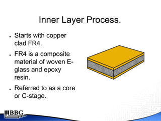
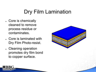
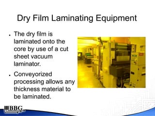
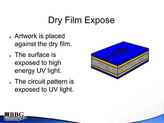
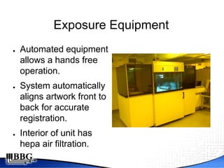
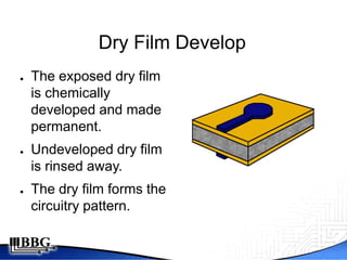
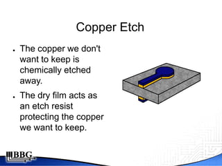
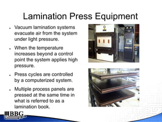
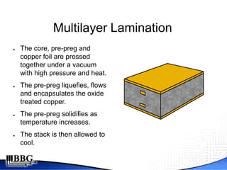
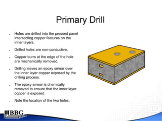
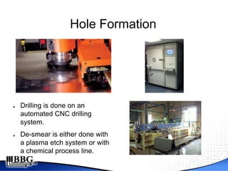
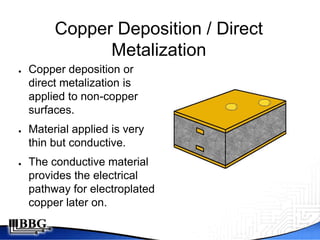
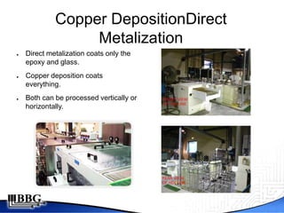
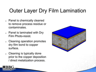
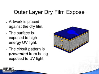
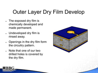
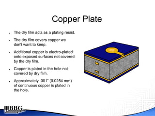
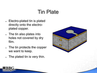
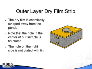
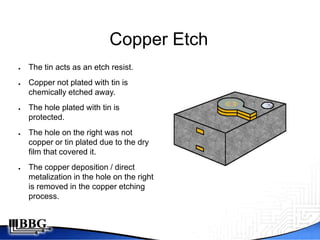
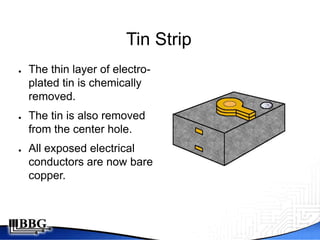
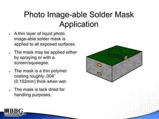
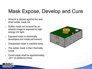
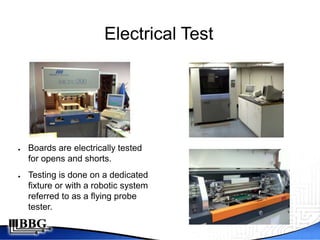
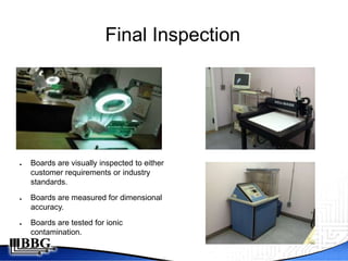
PCB 101

The Basics of Building a Printed Circuit Board.


                Presented by
                David Duross
             Engineering Director
Inner Layer Process.
●   Starts with copper
    clad FR4.
●   FR4 is a composite
    material of woven E-
    glass and epoxy
    resin.
●   Referred to as a core
    or C-stage.
Dry Film Lamination
●   Core is chemically
    cleaned to remove
    process residue or
    contaminates.
●   Core is laminated with
    Dry Film Photo-resist.
●   Cleaning operation
    promotes dry film bond
    to copper surface.
Dry Film Laminating Equipment
●   The dry film is
    laminated onto the
    core by use of a cut
    sheet vacuum
    laminator.
●   Conveyorized
    processing allows any
    thickness material to
    be laminated.
Dry Film Expose
●   Artwork is placed
    against the dry film.
●   The surface is
    exposed to high
    energy UV light.
●   The circuit pattern is
    exposed to UV light.
Exposure Equipment
●   Automated equipment
    allows a hands free
    operation.
●   System automatically
    aligns artwork front to
    back for accurate
    registration.
●   Interior of unit has
    hepa air filtration.
Dry Film Develop
●   The exposed dry film
    is chemically
    developed and made
    permanent.
●   Undeveloped dry film
    is rinsed away.
●   The dry film forms the
    circuitry pattern.
Copper Etch
●   The copper we don't
    want to keep is
    chemically etched
    away.
●   The dry film acts as
    an etch resist
    protecting the copper
    we want to keep.
Dry Film Strip
●   The dry film photo-
    resist is chemically
    removed.
●   The inner layer
    circuitry pattern is
    now formed.
Post Etch Punch and AOI
●   Post etch punch
    automatically adds
    mechanical alignment
    positions to the core in the
    form of four slots.
●   Provides accurate alignment
    for multiple cores.
●   Panels are then inspected on
    a system known as an AOI.
●   AOI is short for Automatic
    Optical Inspection.
Oxide Treatment
●   Copper is a very smooth
    surface.
●   The copper surface needs
    to be roughened up to
    promote bonding to epoxy
    resin later on. Oxide
    treatment does this.
●   FR4 after copper etch is
    rough enough to provide a
    good bonding surface.
Multilayer Lamination
●   The core forms the inner
    layers.
●   Sheets of pre-preg (B-
    stage) are placed against
    the core.
●   Copper foil is then placed
    against the pre-preg.
●   The copper foil forms the
    outer layers of the printed
    circuit board.
Lamination Press Equipment
●   Vacuum lamination systems
    evacuate air from the system
    under light pressure.
●   When the temperature
    increases beyond a control
    point the system applies high
    pressure.
●   Press cycles are controlled
    by a computerized system.
●   Multiple process panels are
    pressed at the same time in
    what is referred to as a
    lamination book.
Multilayer Lamination
●   The core, pre-preg and
    copper foil are pressed
    together under a vacuum
    with high pressure and heat.
●   The pre-preg liquefies, flows
    and encapsulates the oxide
    treated copper.
●   The pre-preg solidifies as
    temperature increases.
●   The stack is then allowed to
    cool.
Primary Drill
●   Holes are drilled into the pressed panel
    intersecting copper features on the
    inner layers.
●   Drilled holes are non-conductive.
●   Copper burrs at the edge of the hole
    are mechanically removed.
●   Drilling leaves an epoxy smear over
    the inner layer copper exposed by the
    drilling process.
●   The epoxy smear is chemically
    removed to ensure that the inner layer
    copper is exposed.
●   Note the location of the two holes.
Hole Formation


●   Drilling is done on an
    automated CNC drilling
    system.
●   De-smear is either done with
    a plasma etch system or with
    a chemical process line.
Copper Deposition / Direct
               Metalization
●   Copper deposition or
    direct metalization is
    applied to non-copper
    surfaces.
●   Material applied is very
    thin but conductive.
●   The conductive material
    provides the electrical
    pathway for electroplated
    copper later on.
Copper DepositionDirect
                  Metalization
●   Direct metalization coats only the
    epoxy and glass.
●   Copper deposition coats
    everything.
●   Both can be processed vertically or
    horizontally.
Outer Layer Dry Film Lamination
●   Panel is chemically cleaned
    to remove process residue or
    contaminates.
●   Panel is laminated with Dry
    Film Photo-resist.
●   Cleaning operation promotes
    dry film bond to copper
    surface.
●   Cleaning is typically done
    prior to the copper deposition
    / direct metalization process.
Outer Layer Dry Film Expose
●   Artwork is placed
    against the dry film.
●   The surface is
    exposed to high
    energy UV light.
●   The circuit pattern is
    prevented from being
    exposed to UV light.
Outer Layer Dry Film Develop
●   The exposed dry film is
    chemically developed and
    made permanent.
●   Undeveloped dry film is
    rinsed away.
●   Openings in the dry film form
    the circuitry pattern.
●   Note that one of our two
    drilled holes is covered by
    the dry film.
Copper Plate
●   The dry film acts as a plating resist.
●   The dry film covers copper we
    don't want to keep.
●   Additional copper is electro-plated
    onto exposed surfaces not covered
    by the dry film.
●   Copper is plated in the hole not
    covered by dry film.
●   Approximately .001” (0.0254 mm)
    of continuous copper is plated in
    the hole.
Tin Plate
●   Electro-plated tin is plated
    directly onto the electro-
    plated copper.
●   The tin also plates into
    holes not covered by dry
    film.
●   The tin protects the copper
    we want to keep.
●   The plated tin is very thin.
Outer Layer Dry Film Strip
●   The dry film is chemically
    stripped away from the
    panel.
●   Note that the hole in the
    center of our sample is
    tin plated.
●   The hole on the right
    side is not plated with tin.
Copper Etch
●   The tin acts as an etch resist.
●   Copper not plated with tin is
    chemically etched away.
●   The hole plated with tin is
    protected.
●   The hole on the right was not
    copper or tin plated due to the dry
    film that covered it.
●   The copper deposition / direct
    metalization in the hole on the right
    is removed in the copper etching
    process.
Tin Strip
●   The thin layer of electro-
    plated tin is chemically
    removed.
●   The tin is also removed
    from the center hole.
●   All exposed electrical
    conductors are now bare
    copper.
Photo Image-able Solder Mask
                  Application
●   A thin layer of liquid photo
    image-able solder mask is
    applied to all exposed surfaces.
●   The mask may be applied either
    by spraying or with a
    screen/squeegee.
●   The mask is a thin polymer
    coating roughly .004”
    (0.102mm) thick when wet.
●   The mask is tack dried for
    handling purposes.
Mask Expose, Develop and Cure
●   Artwork is placed against the tack
    dried solder mask ink.
●   Solder mask not covered by an
    artwork image is exposed to high
    energy UV light.
●   Exposed mask is chemically
    developed and made permanent.
●   Unexposed mask is washed away.
●   The solder mask is then thermally
    cured.
●   Cured mask shall be approximately
    .001” (0.0254mm) thick.
Hot Air Solder Leveling
●   Panels are coated with solder flux.
●   For vertical processing panels are
    dipped into a large solder pot.
●   For horizontal processing panels are
    passed through a solder fountain.
●   Excess solder is shaved off of the
    process panel with hot blowing air
    knives.
●   Solder is typically 200 micro-inches in
    thickness minimum.
●   Solder-ability is the acceptance criteria.
Component Markings
●   Component markings are
    applied with non-conductive
    inks.
●   Markings can be any color.
    White is the most common.
●   Inks can be applied by a
    screen/squeegee set-up or
    with an ink-jet printer.
●   Markings typically indicate
    component placement and
    orientation.
Marking Equipment
●   Ink jet printing applies a white
    epoxy ink sprayed as a final image
    and UV tack dried as the ink is
    applied.
●   Silkscreening relies on pulling a
    squeegee across a mesh.
    Openings in the mesh match the
    marking features.
●   Both techniques require the ink to
    be baked to ensure final cure.
●   UV cure-able inks are available as
    well.
Final Fabrication


●   Individual boards are routed and or
    scored free from the process panel.
●   Specialty milling such as counter bores
    and sinks may be added at this step.
●   Boards are rinsed free of process
    debris and dried.
Electrical Test


●   Boards are electrically tested
    for opens and shorts.
●   Testing is done on a dedicated
    fixture or with a robotic system
    referred to as a flying probe
    tester.
Final Inspection


●   Boards are visually inspected to either
    customer requirements or industry
    standards.
●   Boards are measured for dimensional
    accuracy.
●   Boards are tested for ionic
    contamination.
End

Pcb 101

  • 2.
    PCB 101 The Basicsof Building a Printed Circuit Board. Presented by David Duross Engineering Director
  • 3.
    Inner Layer Process. ● Starts with copper clad FR4. ● FR4 is a composite material of woven E- glass and epoxy resin. ● Referred to as a core or C-stage.
  • 4.
    Dry Film Lamination ● Core is chemically cleaned to remove process residue or contaminates. ● Core is laminated with Dry Film Photo-resist. ● Cleaning operation promotes dry film bond to copper surface.
  • 5.
    Dry Film LaminatingEquipment ● The dry film is laminated onto the core by use of a cut sheet vacuum laminator. ● Conveyorized processing allows any thickness material to be laminated.
  • 6.
    Dry Film Expose ● Artwork is placed against the dry film. ● The surface is exposed to high energy UV light. ● The circuit pattern is exposed to UV light.
  • 7.
    Exposure Equipment ● Automated equipment allows a hands free operation. ● System automatically aligns artwork front to back for accurate registration. ● Interior of unit has hepa air filtration.
  • 8.
    Dry Film Develop ● The exposed dry film is chemically developed and made permanent. ● Undeveloped dry film is rinsed away. ● The dry film forms the circuitry pattern.
  • 9.
    Copper Etch ● The copper we don't want to keep is chemically etched away. ● The dry film acts as an etch resist protecting the copper we want to keep.
  • 10.
    Dry Film Strip ● The dry film photo- resist is chemically removed. ● The inner layer circuitry pattern is now formed.
  • 11.
    Post Etch Punchand AOI ● Post etch punch automatically adds mechanical alignment positions to the core in the form of four slots. ● Provides accurate alignment for multiple cores. ● Panels are then inspected on a system known as an AOI. ● AOI is short for Automatic Optical Inspection.
  • 12.
    Oxide Treatment ● Copper is a very smooth surface. ● The copper surface needs to be roughened up to promote bonding to epoxy resin later on. Oxide treatment does this. ● FR4 after copper etch is rough enough to provide a good bonding surface.
  • 13.
    Multilayer Lamination ● The core forms the inner layers. ● Sheets of pre-preg (B- stage) are placed against the core. ● Copper foil is then placed against the pre-preg. ● The copper foil forms the outer layers of the printed circuit board.
  • 14.
    Lamination Press Equipment ● Vacuum lamination systems evacuate air from the system under light pressure. ● When the temperature increases beyond a control point the system applies high pressure. ● Press cycles are controlled by a computerized system. ● Multiple process panels are pressed at the same time in what is referred to as a lamination book.
  • 15.
    Multilayer Lamination ● The core, pre-preg and copper foil are pressed together under a vacuum with high pressure and heat. ● The pre-preg liquefies, flows and encapsulates the oxide treated copper. ● The pre-preg solidifies as temperature increases. ● The stack is then allowed to cool.
  • 16.
    Primary Drill ● Holes are drilled into the pressed panel intersecting copper features on the inner layers. ● Drilled holes are non-conductive. ● Copper burrs at the edge of the hole are mechanically removed. ● Drilling leaves an epoxy smear over the inner layer copper exposed by the drilling process. ● The epoxy smear is chemically removed to ensure that the inner layer copper is exposed. ● Note the location of the two holes.
  • 17.
    Hole Formation ● Drilling is done on an automated CNC drilling system. ● De-smear is either done with a plasma etch system or with a chemical process line.
  • 18.
    Copper Deposition /Direct Metalization ● Copper deposition or direct metalization is applied to non-copper surfaces. ● Material applied is very thin but conductive. ● The conductive material provides the electrical pathway for electroplated copper later on.
  • 19.
    Copper DepositionDirect Metalization ● Direct metalization coats only the epoxy and glass. ● Copper deposition coats everything. ● Both can be processed vertically or horizontally.
  • 20.
    Outer Layer DryFilm Lamination ● Panel is chemically cleaned to remove process residue or contaminates. ● Panel is laminated with Dry Film Photo-resist. ● Cleaning operation promotes dry film bond to copper surface. ● Cleaning is typically done prior to the copper deposition / direct metalization process.
  • 21.
    Outer Layer DryFilm Expose ● Artwork is placed against the dry film. ● The surface is exposed to high energy UV light. ● The circuit pattern is prevented from being exposed to UV light.
  • 22.
    Outer Layer DryFilm Develop ● The exposed dry film is chemically developed and made permanent. ● Undeveloped dry film is rinsed away. ● Openings in the dry film form the circuitry pattern. ● Note that one of our two drilled holes is covered by the dry film.
  • 23.
    Copper Plate ● The dry film acts as a plating resist. ● The dry film covers copper we don't want to keep. ● Additional copper is electro-plated onto exposed surfaces not covered by the dry film. ● Copper is plated in the hole not covered by dry film. ● Approximately .001” (0.0254 mm) of continuous copper is plated in the hole.
  • 24.
    Tin Plate ● Electro-plated tin is plated directly onto the electro- plated copper. ● The tin also plates into holes not covered by dry film. ● The tin protects the copper we want to keep. ● The plated tin is very thin.
  • 25.
    Outer Layer DryFilm Strip ● The dry film is chemically stripped away from the panel. ● Note that the hole in the center of our sample is tin plated. ● The hole on the right side is not plated with tin.
  • 26.
    Copper Etch ● The tin acts as an etch resist. ● Copper not plated with tin is chemically etched away. ● The hole plated with tin is protected. ● The hole on the right was not copper or tin plated due to the dry film that covered it. ● The copper deposition / direct metalization in the hole on the right is removed in the copper etching process.
  • 27.
    Tin Strip ● The thin layer of electro- plated tin is chemically removed. ● The tin is also removed from the center hole. ● All exposed electrical conductors are now bare copper.
  • 28.
    Photo Image-able SolderMask Application ● A thin layer of liquid photo image-able solder mask is applied to all exposed surfaces. ● The mask may be applied either by spraying or with a screen/squeegee. ● The mask is a thin polymer coating roughly .004” (0.102mm) thick when wet. ● The mask is tack dried for handling purposes.
  • 29.
    Mask Expose, Developand Cure ● Artwork is placed against the tack dried solder mask ink. ● Solder mask not covered by an artwork image is exposed to high energy UV light. ● Exposed mask is chemically developed and made permanent. ● Unexposed mask is washed away. ● The solder mask is then thermally cured. ● Cured mask shall be approximately .001” (0.0254mm) thick.
  • 30.
    Hot Air SolderLeveling ● Panels are coated with solder flux. ● For vertical processing panels are dipped into a large solder pot. ● For horizontal processing panels are passed through a solder fountain. ● Excess solder is shaved off of the process panel with hot blowing air knives. ● Solder is typically 200 micro-inches in thickness minimum. ● Solder-ability is the acceptance criteria.
  • 31.
    Component Markings ● Component markings are applied with non-conductive inks. ● Markings can be any color. White is the most common. ● Inks can be applied by a screen/squeegee set-up or with an ink-jet printer. ● Markings typically indicate component placement and orientation.
  • 32.
    Marking Equipment ● Ink jet printing applies a white epoxy ink sprayed as a final image and UV tack dried as the ink is applied. ● Silkscreening relies on pulling a squeegee across a mesh. Openings in the mesh match the marking features. ● Both techniques require the ink to be baked to ensure final cure. ● UV cure-able inks are available as well.
  • 33.
    Final Fabrication ● Individual boards are routed and or scored free from the process panel. ● Specialty milling such as counter bores and sinks may be added at this step. ● Boards are rinsed free of process debris and dried.
  • 34.
    Electrical Test ● Boards are electrically tested for opens and shorts. ● Testing is done on a dedicated fixture or with a robotic system referred to as a flying probe tester.
  • 35.
    Final Inspection ● Boards are visually inspected to either customer requirements or industry standards. ● Boards are measured for dimensional accuracy. ● Boards are tested for ionic contamination.
  • 36.