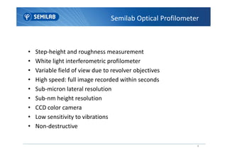
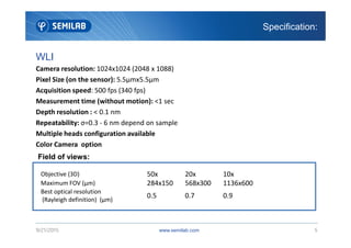
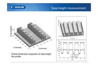
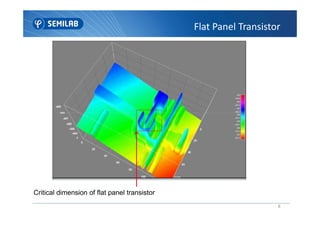
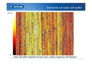
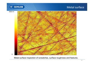
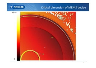
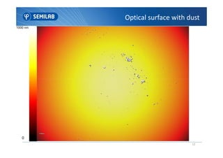
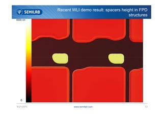
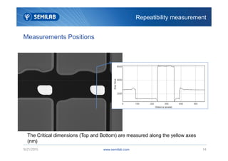
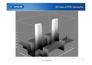
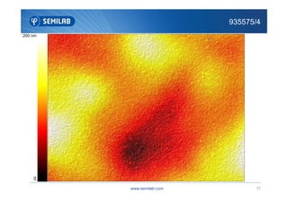
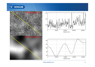
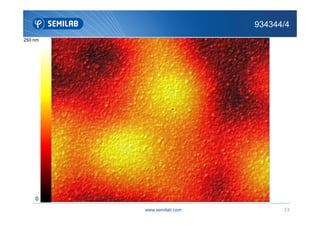
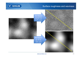
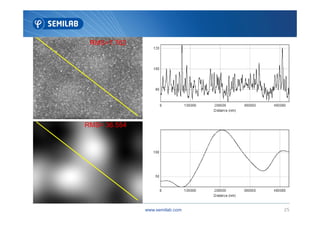
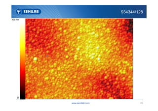
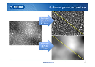
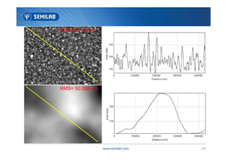
SlideShare a Scribd company logo
WhiteWhiteWhiteWhite LightLightLightLight InterferometryInterferometryInterferometryInterferometry
3D Profilometer
Theory background
• Interferometer uses the superposition principle to combine waves in a
way to extract information from the wave fronts.
• The position of the zero order interference fringe is independent of
wavelength
• A broadband “white light” source is used to illuminate the test and
reference surfaces
2
reference surfaces
• The reference beam is reflected by the reference mirror, while the
measurement beam is reflected or scattered from the test surface.
• Reconstruction of the surface based on the fringes snapped by the
camera
Intensity = A + B cos(φ) φ ∽ z 3D topographic
image of the
object surface
Light
Plane
Mirau microscope objective
3
Convergent
lens
Plane
reference
mirror
Reference
surface
z
Object surface
Interferences
• Step-height and roughness measurement
• White light interferometric profilometer
• Variable field of view due to revolver objectives
• High speed: full image recorded within seconds
Semilab Optical Profilometer
4
• High speed: full image recorded within seconds
• Sub-micron lateral resolution
• Sub-nm height resolution
• CCD color camera
• Low sensitivity to vibrations
• Non-destructive
WLI
Camera resolution: 1024x1024 (2048 x 1088)
Pixel Size (on the sensor): 5.5µmx5.5µm
Acquisition speed: 500 fps (340 fps)
Measurement time (without motion): <1 sec
Depth resolution : < 0.1 nm
Repeatability: σ=0.3 - 6 nm depend on sample
Specification:
www.semilab.com
Repeatability: σ=0.3 - 6 nm depend on sample
Multiple heads configuration available
Color Camera option
9/21/2015 5
Objective (3D) 50x 20x 10x
Maximum FOV (µm) 284x150 568x300 1136x600
Best optical resolution
(Rayleigh definition) (µm)
0.5 0.7 0.9
Field of views:
Application examples
Step-height measurement
7
Critical dimension inspection of step-height
like profile
Flat Panel Transistor
8
Critical dimension of flat panel transistor
Diamond cut solar cell wafer
1700 nm
9
Solar cell wafer inspection of saw mark, surface roughness and features.
0
Metal surface
3000 nm
10
Metal surface inspection of screatches, surface roughness and features.
0
Critical dimension of MEMS device
400 nm
11
0
Optical surface with dust
1000 nm
12
0
Recent WLI demo result: spacers height in FPD
structures
6000 nm
www.semilab.com9/21/2015 13
0
Measurements Positions
Repeatibility measurement
www.semilab.com9/21/2015 14
The Critical dimensions (Top and Bottom) are measured along the yellow axes
(nm)
3D view of FPD structures
www.semilab.com 15
Application examples
Surface roughness
935575/4
200 nm
www.semilab.com 17
0
Surface roughness and waviness
200 nm
RMS=4.797 nm
www.semilab.com 18
0
RMS=36.273 nm
Surface roughness and waviness II.
RMS=4.797 nm
www.semilab.com 19
RMS=36.273 nm
9355755/128
250 nm
www.semilab.com 20
0
Surface roughness and waviness
Bandpass
(0.027 to
2.75 um)
www.semilab.com 21
Bandpass
(2.75 to
555 um)
RMS=9.433 nm
www.semilab.com 22
RMS= 27.298 nm
934344/4
250 nm
www.semilab.com 23
0
Surface roughness and waviness
Bandpass
(0.027 to
2.75 um)
www.semilab.com 24
Bandpass
(2.75 to
555 um)
RMS=7.762
www.semilab.com 25
RMS= 36.554
934344/128
400 nm
www.semilab.com 26
0
Surface roughness and waviness
Bandpass
(0.027 to
2.75 um)
www.semilab.com 27
Bandpass
(2.75 to
555 um)
RMS=28.122nm
www.semilab.com 28
RMS= 50.088 nm
• Semilab is capable to deliver state of art 3d surface profiling metrology using white
light interferometry
• Best resolution available : high resolution camera can deliver data up to 2 Megapixels,
in less than 3s aquisition time
Conclusions
www.semilab.com
in less than 3s aquisition time
• Semilab wli technology proved to work for various industrial applications in the flat
panel, solar cell and semiconductor area
• Excellent repeatability is proven to be in the range of few nm-s
29

More Related Content

What's hot

lasers SOLID STATE LASERS .
 lasers SOLID STATE LASERS . lasers SOLID STATE LASERS .
lasers SOLID STATE LASERS .
sana shaikh
 
Atomic Force Microscope: Fundamental Principles
Atomic Force Microscope: Fundamental PrinciplesAtomic Force Microscope: Fundamental Principles
Atomic Force Microscope: Fundamental Principles
Joy Bhattacharjee
 
Piezoelectric materials-final
Piezoelectric materials-finalPiezoelectric materials-final
Piezoelectric materials-final
foysalmd
 
Infrared thermography
Infrared thermographyInfrared thermography
Molecular Beam Epitaxy
Molecular Beam EpitaxyMolecular Beam Epitaxy
Molecular Beam Epitaxy
Deepak Rajput
 
Nano tribology.pptx
Nano tribology.pptxNano tribology.pptx
Nano tribology.pptx
Mohammad Aamir
 
Basic Introduction of XANES and EXAFS
Basic Introduction of XANES and EXAFSBasic Introduction of XANES and EXAFS
Basic Introduction of XANES and EXAFS
Amlan Roy
 
Spintronics
SpintronicsSpintronics
Spintronics
Mustahid Ali
 
Giant magnetoresistance ppt
Giant magnetoresistance pptGiant magnetoresistance ppt
Giant magnetoresistance ppt
tedoado
 
VSM
VSM VSM
Technology of chemical-mechanical polishing (CMP) of material surfaces
Technology of chemical-mechanical polishing (CMP) of material surfacesTechnology of chemical-mechanical polishing (CMP) of material surfaces
Technology of chemical-mechanical polishing (CMP) of material surfaces
Максим Зарезов
 
BCS theory
BCS theoryBCS theory
BCS theory
Dr. Ramya K
 
Microactuators-MEMS
Microactuators-MEMSMicroactuators-MEMS
Microactuators-MEMS
Yuga Aravind Kumar
 
Infrared thermography
Infrared thermographyInfrared thermography
Infrared thermography
Naila Syed
 
Fermi energy
Fermi energyFermi energy
Fermi energy
Hirunika Athtanayeke
 
Highly efficient organic devices.
Highly efficient organic devices.Highly efficient organic devices.
Highly efficient organic devices.
Sociedade Brasileira de Pesquisa em Materiais
 
Thermocouple gauge & pirani gauge
Thermocouple gauge & pirani gauge  Thermocouple gauge & pirani gauge
Thermocouple gauge & pirani gauge
Naveen Choudhary
 

What's hot (20)

lasers SOLID STATE LASERS .
 lasers SOLID STATE LASERS . lasers SOLID STATE LASERS .
lasers SOLID STATE LASERS .
 
Atomic Force Microscope: Fundamental Principles
Atomic Force Microscope: Fundamental PrinciplesAtomic Force Microscope: Fundamental Principles
Atomic Force Microscope: Fundamental Principles
 
Squids
SquidsSquids
Squids
 
Piezoelectric materials-final
Piezoelectric materials-finalPiezoelectric materials-final
Piezoelectric materials-final
 
Infrared thermography
Infrared thermographyInfrared thermography
Infrared thermography
 
Molecular Beam Epitaxy
Molecular Beam EpitaxyMolecular Beam Epitaxy
Molecular Beam Epitaxy
 
Nano tribology.pptx
Nano tribology.pptxNano tribology.pptx
Nano tribology.pptx
 
Basic Introduction of XANES and EXAFS
Basic Introduction of XANES and EXAFSBasic Introduction of XANES and EXAFS
Basic Introduction of XANES and EXAFS
 
Spintronics
SpintronicsSpintronics
Spintronics
 
Giant magnetoresistance ppt
Giant magnetoresistance pptGiant magnetoresistance ppt
Giant magnetoresistance ppt
 
VSM
VSM VSM
VSM
 
Technology of chemical-mechanical polishing (CMP) of material surfaces
Technology of chemical-mechanical polishing (CMP) of material surfacesTechnology of chemical-mechanical polishing (CMP) of material surfaces
Technology of chemical-mechanical polishing (CMP) of material surfaces
 
BCS theory
BCS theoryBCS theory
BCS theory
 
Microactuators-MEMS
Microactuators-MEMSMicroactuators-MEMS
Microactuators-MEMS
 
Infrared thermography
Infrared thermographyInfrared thermography
Infrared thermography
 
Fermi energy
Fermi energyFermi energy
Fermi energy
 
Photodetectors
PhotodetectorsPhotodetectors
Photodetectors
 
Highly efficient organic devices.
Highly efficient organic devices.Highly efficient organic devices.
Highly efficient organic devices.
 
Thermocouple gauge & pirani gauge
Thermocouple gauge & pirani gauge  Thermocouple gauge & pirani gauge
Thermocouple gauge & pirani gauge
 
Spintronics ppt
Spintronics pptSpintronics ppt
Spintronics ppt
 

Similar to White Light Interferometry 3D Surface Profiler

Nanolithography
NanolithographyNanolithography
Nanolithography
karthika namboothiri
 
Nanonics - Raman MultiProbe
Nanonics - Raman MultiProbeNanonics - Raman MultiProbe
Nanonics - Raman MultiProbe
Nanonics
 
Introduction to X-Ray Imaging for Industrial Applications
Introduction to X-Ray Imaging for Industrial ApplicationsIntroduction to X-Ray Imaging for Industrial Applications
Introduction to X-Ray Imaging for Industrial Applications
MoviMED - Custom Imaging Solutions
 
(Public) se 2000-presentation_20140120
(Public) se 2000-presentation_20140120(Public) se 2000-presentation_20140120
(Public) se 2000-presentation_20140120
Nor Syazreena Abu Talib
 
UNIT-V.pptx
UNIT-V.pptxUNIT-V.pptx
UNIT-V.pptx
Maniyarasan M
 
MM-UNIT-V.pptx
MM-UNIT-V.pptxMM-UNIT-V.pptx
MM-UNIT-V.pptx
GunaSekaran958261
 
5.1. lithography 1,2.final 2013
5.1. lithography 1,2.final 20135.1. lithography 1,2.final 2013
5.1. lithography 1,2.final 2013
Bhargav Veepuri
 
5.2. lithography 3,4,5 final,2013
5.2. lithography 3,4,5 final,20135.2. lithography 3,4,5 final,2013
5.2. lithography 3,4,5 final,2013
Bhargav Veepuri
 
Cbct
CbctCbct
3D Surface characterisation - Atomic Force and Scanning Electron Microscopy...
3D Surface characterisation -   Atomic Force and Scanning Electron Microscopy...3D Surface characterisation -   Atomic Force and Scanning Electron Microscopy...
3D Surface characterisation - Atomic Force and Scanning Electron Microscopy...
Daniel Thomas
 
Photonics Applications - Silicon - Nanonics
Photonics Applications - Silicon - NanonicsPhotonics Applications - Silicon - Nanonics
Photonics Applications - Silicon - Nanonics
David Lewis
 
COBALT MICROSTRUCTURE BY DC MAGNETRON SPUTTERING
COBALT MICROSTRUCTURE BY DC MAGNETRON SPUTTERINGCOBALT MICROSTRUCTURE BY DC MAGNETRON SPUTTERING
COBALT MICROSTRUCTURE BY DC MAGNETRON SPUTTERING
HHV SOLAR Pvt Ltd
 
Measurement techniques in micro machining PDF by badebhau4@gmail.com
Measurement techniques in micro machining PDF by badebhau4@gmail.comMeasurement techniques in micro machining PDF by badebhau4@gmail.com
Measurement techniques in micro machining PDF by badebhau4@gmail.com
Er. Bade Bhausaheb
 
Material characterisations
Material characterisationsMaterial characterisations
Material characterisations
chandan94sahu
 
Improvement of Surface Roughness of Nickel Alloy Specimen by Removing Recast ...
Improvement of Surface Roughness of Nickel Alloy Specimen by Removing Recast ...Improvement of Surface Roughness of Nickel Alloy Specimen by Removing Recast ...
Improvement of Surface Roughness of Nickel Alloy Specimen by Removing Recast ...
IJMER
 
3D Scanners and their Economic Feasibility
3D Scanners and their Economic Feasibility3D Scanners and their Economic Feasibility
3D Scanners and their Economic Feasibility
Jeffrey Funk
 
Nanophotonic Characterization in the Century of Photonics
Nanophotonic Characterization in the Century of PhotonicsNanophotonic Characterization in the Century of Photonics
Nanophotonic Characterization in the Century of Photonics
Nanonics Imaging Ltd.
 
Digital Image Correlation Presentation
Digital Image Correlation PresentationDigital Image Correlation Presentation
Digital Image Correlation Presentation
trilionqualitysystems
 
極紫外線散射儀於先進製程檢測應用
極紫外線散射儀於先進製程檢測應用極紫外線散射儀於先進製程檢測應用
極紫外線散射儀於先進製程檢測應用
CHENHuiMei
 
22UPH101_Unit-1_3D Profiling.pdf
22UPH101_Unit-1_3D Profiling.pdf22UPH101_Unit-1_3D Profiling.pdf
22UPH101_Unit-1_3D Profiling.pdf
Kishors41
 

Similar to White Light Interferometry 3D Surface Profiler (20)

Nanolithography
NanolithographyNanolithography
Nanolithography
 
Nanonics - Raman MultiProbe
Nanonics - Raman MultiProbeNanonics - Raman MultiProbe
Nanonics - Raman MultiProbe
 
Introduction to X-Ray Imaging for Industrial Applications
Introduction to X-Ray Imaging for Industrial ApplicationsIntroduction to X-Ray Imaging for Industrial Applications
Introduction to X-Ray Imaging for Industrial Applications
 
(Public) se 2000-presentation_20140120
(Public) se 2000-presentation_20140120(Public) se 2000-presentation_20140120
(Public) se 2000-presentation_20140120
 
UNIT-V.pptx
UNIT-V.pptxUNIT-V.pptx
UNIT-V.pptx
 
MM-UNIT-V.pptx
MM-UNIT-V.pptxMM-UNIT-V.pptx
MM-UNIT-V.pptx
 
5.1. lithography 1,2.final 2013
5.1. lithography 1,2.final 20135.1. lithography 1,2.final 2013
5.1. lithography 1,2.final 2013
 
5.2. lithography 3,4,5 final,2013
5.2. lithography 3,4,5 final,20135.2. lithography 3,4,5 final,2013
5.2. lithography 3,4,5 final,2013
 
Cbct
CbctCbct
Cbct
 
3D Surface characterisation - Atomic Force and Scanning Electron Microscopy...
3D Surface characterisation -   Atomic Force and Scanning Electron Microscopy...3D Surface characterisation -   Atomic Force and Scanning Electron Microscopy...
3D Surface characterisation - Atomic Force and Scanning Electron Microscopy...
 
Photonics Applications - Silicon - Nanonics
Photonics Applications - Silicon - NanonicsPhotonics Applications - Silicon - Nanonics
Photonics Applications - Silicon - Nanonics
 
COBALT MICROSTRUCTURE BY DC MAGNETRON SPUTTERING
COBALT MICROSTRUCTURE BY DC MAGNETRON SPUTTERINGCOBALT MICROSTRUCTURE BY DC MAGNETRON SPUTTERING
COBALT MICROSTRUCTURE BY DC MAGNETRON SPUTTERING
 
Measurement techniques in micro machining PDF by badebhau4@gmail.com
Measurement techniques in micro machining PDF by badebhau4@gmail.comMeasurement techniques in micro machining PDF by badebhau4@gmail.com
Measurement techniques in micro machining PDF by badebhau4@gmail.com
 
Material characterisations
Material characterisationsMaterial characterisations
Material characterisations
 
Improvement of Surface Roughness of Nickel Alloy Specimen by Removing Recast ...
Improvement of Surface Roughness of Nickel Alloy Specimen by Removing Recast ...Improvement of Surface Roughness of Nickel Alloy Specimen by Removing Recast ...
Improvement of Surface Roughness of Nickel Alloy Specimen by Removing Recast ...
 
3D Scanners and their Economic Feasibility
3D Scanners and their Economic Feasibility3D Scanners and their Economic Feasibility
3D Scanners and their Economic Feasibility
 
Nanophotonic Characterization in the Century of Photonics
Nanophotonic Characterization in the Century of PhotonicsNanophotonic Characterization in the Century of Photonics
Nanophotonic Characterization in the Century of Photonics
 
Digital Image Correlation Presentation
Digital Image Correlation PresentationDigital Image Correlation Presentation
Digital Image Correlation Presentation
 
極紫外線散射儀於先進製程檢測應用
極紫外線散射儀於先進製程檢測應用極紫外線散射儀於先進製程檢測應用
極紫外線散射儀於先進製程檢測應用
 
22UPH101_Unit-1_3D Profiling.pdf
22UPH101_Unit-1_3D Profiling.pdf22UPH101_Unit-1_3D Profiling.pdf
22UPH101_Unit-1_3D Profiling.pdf
 

White Light Interferometry 3D Surface Profiler