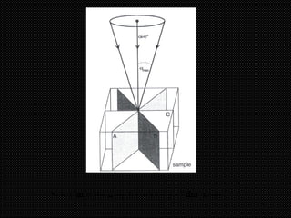
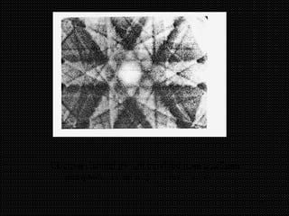
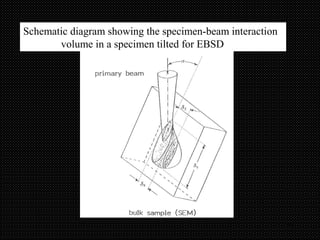
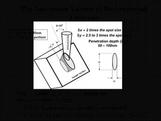
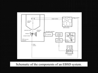
Mohammed Zeeshan
BT/PE/1601/001
1
2
Microtexture analysis:Microtexture analysis:
Electron DiffractionElectron Diffraction
in the SEMin the SEM
Texture And Microstructure
3
Different types of microtexture techniques for obtaining
crystallographic information.
ELECTRONS
SEM-based TEM-based
ECP EBSD SADP KikuchiKoseel
4
SEM-based Microtexture Techniques
5
Kossel Technique:
• This technique is based on using electron beam to generate
X-rays within the sample under investigation.
• Need high acceleration voltage. About 2-3 times larger
than the critical voltage to produce characteristic X-ray Kα
radiation.
• These are recorded on an X-ray sensitive film (see Fig. next
slide).
6
(a) Diagram illustrating the formation of Kossel patterns in
reflection; (b) Kossel pattern from titanium
(a) (b)
7
• Because the wavelength of X-rays (Kossel technique) is
much larger than that of electrons, all Bragg angles θ
between 0o
and 90o
may occur.
• Therefore the resulting projection lines on the film plane
are strongly curved as seen in Figure 22(b).
8
• Can be used to determine crystallographic orientation,
structural type (image contrast), unit cell size, or a measure
of the crystal perfection.
• Although we cannot obtain diffraction spot patterns in the
SEM, as we can in the TEM, we can make use of electron
channeling for diffraction patterns.
Electron Channeling Pattern (ECP):
9
• For orientation determination, the electron beam in the
SEM is focused on the sample site to be analyzed.
• The beam is tilted at this position by an angle α, and
rocked on the specimen surface, as shown in Figure, next
slide.
10
Schematic showing the rocking of the beam.
11
• The resulting pattern is known as selected area channeling
pattern (SACP).
• Although there method of formation are not identical, the
SACPs are geometrically similar to TEM Kikuchi patterns
and EBSD patterns.
• Therefore, they are analyzed in a similar manner.
• They are composed of bright bands of a given thickness
representing distinct crystallographic planes (see Figs. next
slides).
12
Schematic showing the resulting pattern.
13
Electron channel pattern obtained from a gallium
phosphide crystal of (111) orientation.
14
Electron channel pattern of a recrystallized grain in a partially
recrystallized Al-Fe-Si sample.
15
• In general, the spatial resolution of this technique is limited
to ∼ 10 µm.
• Also, the technique is very sensitive to lattice defects.
Therefore, only recrystallized or recovered microstructures
have been successfully analyzed.
16
Schematic diagram showing the specimen-beam interaction
volume in a specimen tilted for EBSD
17
The Interaction Volume of Backscattered
Electrons
• When Considering the Issue of Interaction
VolumePenetration Depth:
– Will the beam penetrate through the precipitates?
– Will there be pattern overlapping from Austenite Matrix?
δx ≈ 2 times the spot size
δy ≈ 2.5 to 3 times the spot size
Penetration depth (δz):
50 – 100nm
Spot Size: 30nm
15kV, 60µm Aperture
18
• The main effect of tilting the specimen is to reduce the path
length of electrons, which have been backscattered by
lattice planes.
• Therefore, when compared to flat specimen, more of these
electrons undergo diffraction, and escape from the
specimen before being absorbed.
19
Schematic of the components of an EBSD system.
20
Timeline of EBSD development.
21
22
EBSD Specimen Preparation:
• A carefully prepared specimen, with no deformed surface
(top 10-50 nm) layer.
• Specimen preparation is supposed to be uncomplicated, and
similar to that for optical microscopy.
• Since the diffraction zone is shallow, the specimen surface
must no be obscured by:
– mechanical damage due to grinding,
– surface layers due to thick coatings,
– surface undulation due to protruding particles, or
– contamination
23
• Minimization of diamond polishing is necessary in order to
avoid surface damage.
• It may be necessary to avoid some common electropolishes
or etchants, which may deposit films on the surface. A
useful guide is to use TEM electrolytes.
• A combination of etching and mechanical polishing may
be used, especially if OIM is required.
• Final polish in colloidal silica is highly recommended.
24
• Inadequate or inappropriate specimen preparation could
give rise to erroneous data interpretation.
• Acceleration voltage and coating of samples can affect the
quality of diffraction pattern obtained, as can be seen in the
next Figure (a) - (c).
25
Effect of acceleration voltage on the quality of diffraction pattern
of sample with no coating (a) 10 kV accelerating
voltage and (b) 40 kV accelerating voltage.
26
Effect of acceleration voltage on the quality of diffraction
pattern of a coated (5 nm Ni) sample (c) 10 kV
accelerating voltage and (d) 40 kV accelerating
voltage.
27
Some Specimen Preparation Methods
• Heavily Deformed OFHC Copper
– Mechanical polish
– Light diamond polish
– Silica on Vibromet polish
– Etch in 50% Ammonium Hydroxide and 50% Peroxide
– Silica on Vibromet polish
28
Orientation Imaging Microscopy (OIM):
• An Orientation Imaging Micrograph is produced by
successively collecting and indexing Electron
Backscattered Diffraction (EBSD) patterns at point
spaced over a specimen surface in a regular grid.
• The technique is based on electron backscattered
diffraction in the scanning Electron microscope.

Microtexture analysis

  • 1.
  • 2.
    2 Microtexture analysis:Microtexture analysis: ElectronDiffractionElectron Diffraction in the SEMin the SEM Texture And Microstructure
  • 3.
    3 Different types ofmicrotexture techniques for obtaining crystallographic information. ELECTRONS SEM-based TEM-based ECP EBSD SADP KikuchiKoseel
  • 4.
  • 5.
    5 Kossel Technique: • Thistechnique is based on using electron beam to generate X-rays within the sample under investigation. • Need high acceleration voltage. About 2-3 times larger than the critical voltage to produce characteristic X-ray Kα radiation. • These are recorded on an X-ray sensitive film (see Fig. next slide).
  • 6.
    6 (a) Diagram illustratingthe formation of Kossel patterns in reflection; (b) Kossel pattern from titanium (a) (b)
  • 7.
    7 • Because thewavelength of X-rays (Kossel technique) is much larger than that of electrons, all Bragg angles θ between 0o and 90o may occur. • Therefore the resulting projection lines on the film plane are strongly curved as seen in Figure 22(b).
  • 8.
    8 • Can beused to determine crystallographic orientation, structural type (image contrast), unit cell size, or a measure of the crystal perfection. • Although we cannot obtain diffraction spot patterns in the SEM, as we can in the TEM, we can make use of electron channeling for diffraction patterns. Electron Channeling Pattern (ECP):
  • 9.
    9 • For orientationdetermination, the electron beam in the SEM is focused on the sample site to be analyzed. • The beam is tilted at this position by an angle α, and rocked on the specimen surface, as shown in Figure, next slide.
  • 10.
    10 Schematic showing therocking of the beam.
  • 11.
    11 • The resultingpattern is known as selected area channeling pattern (SACP). • Although there method of formation are not identical, the SACPs are geometrically similar to TEM Kikuchi patterns and EBSD patterns. • Therefore, they are analyzed in a similar manner. • They are composed of bright bands of a given thickness representing distinct crystallographic planes (see Figs. next slides).
  • 12.
    12 Schematic showing theresulting pattern.
  • 13.
    13 Electron channel patternobtained from a gallium phosphide crystal of (111) orientation.
  • 14.
    14 Electron channel patternof a recrystallized grain in a partially recrystallized Al-Fe-Si sample.
  • 15.
    15 • In general,the spatial resolution of this technique is limited to ∼ 10 µm. • Also, the technique is very sensitive to lattice defects. Therefore, only recrystallized or recovered microstructures have been successfully analyzed.
  • 16.
    16 Schematic diagram showingthe specimen-beam interaction volume in a specimen tilted for EBSD
  • 17.
    17 The Interaction Volumeof Backscattered Electrons • When Considering the Issue of Interaction VolumePenetration Depth: – Will the beam penetrate through the precipitates? – Will there be pattern overlapping from Austenite Matrix? δx ≈ 2 times the spot size δy ≈ 2.5 to 3 times the spot size Penetration depth (δz): 50 – 100nm Spot Size: 30nm 15kV, 60µm Aperture
  • 18.
    18 • The maineffect of tilting the specimen is to reduce the path length of electrons, which have been backscattered by lattice planes. • Therefore, when compared to flat specimen, more of these electrons undergo diffraction, and escape from the specimen before being absorbed.
  • 19.
    19 Schematic of thecomponents of an EBSD system.
  • 20.
    20 Timeline of EBSDdevelopment.
  • 21.
  • 22.
    22 EBSD Specimen Preparation: •A carefully prepared specimen, with no deformed surface (top 10-50 nm) layer. • Specimen preparation is supposed to be uncomplicated, and similar to that for optical microscopy. • Since the diffraction zone is shallow, the specimen surface must no be obscured by: – mechanical damage due to grinding, – surface layers due to thick coatings, – surface undulation due to protruding particles, or – contamination
  • 23.
    23 • Minimization ofdiamond polishing is necessary in order to avoid surface damage. • It may be necessary to avoid some common electropolishes or etchants, which may deposit films on the surface. A useful guide is to use TEM electrolytes. • A combination of etching and mechanical polishing may be used, especially if OIM is required. • Final polish in colloidal silica is highly recommended.
  • 24.
    24 • Inadequate orinappropriate specimen preparation could give rise to erroneous data interpretation. • Acceleration voltage and coating of samples can affect the quality of diffraction pattern obtained, as can be seen in the next Figure (a) - (c).
  • 25.
    25 Effect of accelerationvoltage on the quality of diffraction pattern of sample with no coating (a) 10 kV accelerating voltage and (b) 40 kV accelerating voltage.
  • 26.
    26 Effect of accelerationvoltage on the quality of diffraction pattern of a coated (5 nm Ni) sample (c) 10 kV accelerating voltage and (d) 40 kV accelerating voltage.
  • 27.
    27 Some Specimen PreparationMethods • Heavily Deformed OFHC Copper – Mechanical polish – Light diamond polish – Silica on Vibromet polish – Etch in 50% Ammonium Hydroxide and 50% Peroxide – Silica on Vibromet polish
  • 28.
    28 Orientation Imaging Microscopy(OIM): • An Orientation Imaging Micrograph is produced by successively collecting and indexing Electron Backscattered Diffraction (EBSD) patterns at point spaced over a specimen surface in a regular grid. • The technique is based on electron backscattered diffraction in the scanning Electron microscope.