
Recommended
Recommended
More Related Content
Similar to TFET 2024.pptx for mtech students of any
Similar to TFET 2024.pptx for mtech students of any (20)
Recently uploaded
Recently uploaded (20)
TFET 2024.pptx for mtech students of any
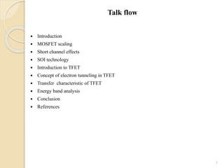
- 1. Talk flow Introduction MOSFET scaling Short channel effects SOI technology Introduction to TFET Concept of electron tunneling in TFET Transfer characteristic of TFET Energy band analysis Conclusion References 1
- 2. Introduction
- 3. MOSFET scaling The reduction of size i.e. dimension of the MOSFETs is commonly referred to as scaling. The design of high density chips in MOS VLSI technology requires that the packing density of MOSFETs used in the circuits is as high as possible and, consequently, that the sizes of the transistors are as small as possible. 3
- 4. Advantages of MOSFET scaling Miniaturization More Functionalities can be realized Cost per IC is reduced Short Channel effects • DIBL ( Drain induced barrier lowering) • Punch through effect • Oxide breakdown 4
- 5. SOI technology Here silicon layer is placed above an electrical insulator. Typically silicon dioxide or sapphire is being used as an insulator. 5 Figure 1. SOI MOSFET
- 6. It is the latest fabrication technique. It is easier & cheaper. Transistors are build on a silicon layer resting on insulating layer of silicon-di- oxide known as BOX (burried oxide). Only a thin layer from a face of the wafer used for making electronic components, the rest essentially serves as mechanical support. Higher speed. Less power consumption. Easier fabrication. Ability to withstand high temp. and high voltage. More electronic devices can be fabricated on same chip (30% more than bulk). It reduces parasitic capacitance when compared to bulk 6 Contd..
- 7. Introduction to TFET Figure 2. Basic structural model of an n-type TFET and a p-type TFET [3].
- 8. Concept of electron tunneling •For thick barrier, both Newtonian and Quantum mechanics say that the electrons cannot cross the barrier. •It can only pass the barrier if it has more energy than the barrier height. Figure 3. Thick barrier width 8
- 9. contd.. • For thin barrier, Newtonian mechanics still says that the electrons cannot cross the barrier. • However, Quantum mechanics says that the electron wave nature will allow it to tunnel through the barrier. Figure 4. Thin barrier width Figure 5. Thin barrier width (electron tunneling) 9
- 10. Transfer characteristic Figure 6. Transfer curve of p-type TFET [3].
- 11. OFF-state ( 0 < VGS < VOFF ) : In this region the TFET has an extremely low current and BTBT is inhibited. VOFF is the gate voltage at which the drain current starts to take off. Subthreshold region (VOFF < VGS <VT ) : In this region the drain current rises rapidly. Super-threshold region (VGS > VT) : In this region the drain current rises with gate voltage at a reduced rate. 11
- 12. Energy Band Analysis: Figure 7. Band diagram of an n-type TFET [3]. 12
- 13. contd.. Figure 8. Band diagram of p-type TFET [3].
- 14. CONCLUSION TFETs are one of the most promising exploratory devices since they exhibit a subthreshold swing lower than 60mv/decade which is a theoritical limit for a conventional MOSFET at room temperature. TFET-based circuits are highly energy efficient than a MOSFET at low to medium performance level. 14
- 15. References 1. W.Y. Choi, B.G. Park, J.D. Lee, and T.J. K. Liu, “Tunneling field-effect transistors (TFETs) with subthreshold swing (SS) less than 60 mV/dec,” IEEE Electron Device Lett., Vol. 28, pp. 743-745, 2007. 2. A.C. Seabaugh and Q. Zhang, “Low-voltage tunnel transistors for beyond CMOS logic,” in Proc. IEEE, vol. 98, pp. 2095-2110, 2010. 3. A.M. Ionescu and H. Riel, “Tunnel field-effect transistors as energyefficient electronic switches,” Nature, vol. 479, pp. 329-337, 2011. 4. A. M. Jossy and T. Vigneswaran, “A perspective review of tunnel field effect transistor with steeper switching behavior and low off current (IOFF) for ultra low power applications,” Int. J. Eng. Technol., Vol. 6, pp. 2092- 2104, 2014. 5. A. Verhulst, W. Vandenberghe, D. Leonelli, R. Rooyackers, A. Vandooren, J. Zhuge, K.-H. Kao, B. Soree, W. Magnusa, M. Fischetti, G. Pourtois, C. Huyghebaert, R. Huang, Y. Wang, K. D. Meyer, W. Dehaene, and M. H. G. Groeseneken, “Si-based tunnel field-effect transistors for low-power nano-electronics,” in 69th Annual Device Research Conference (DRC) IEEE, pp. 193–196, 2011. 6. K. Boucart and A. M. Ionescu, “Double-gate tunnel FET with high-κ gate dielectric,” IEEE Trans. on Electron Devices, vol. 54, pp. 1725– 1733, 2007. 7. Y. Morita, T. Mori, S. Migita, W. Mizubayashi, A. Tanabe, K. Fukuda, T. Matsukawa, K. Endo, S. O’uchi, Y. X. Liu, M. Masahara, and H. Ota, “Performance enhancement of tunnel field-effect transistors by synthetic electric field effect,” IEEE Electron Device Letters, vol. 35, pp. 792–794, 2014. 8. M. Schlosser, K. Bhuwalka, M. Sauter, T. Zilbauer, T. Sulima, and I. Eisele, “Fringing-induced drain current improvement in the tunnel field-effect transistor with high-κ gate dielectrics,” IEEE Trans. on Electron Devices, vol. 56, pp. 100–108, 2009. 9. I. Eisele, H. Lochner, and M. Schlosser, “SiGe tunnel field effect transistors,” ECS Transactions, vol. 16, pp. 961–973, 2008. 10. C. Anghel, P. Chilagani, A. Amara, and A. Vladimirescu, “Tunnel field effect transistor with increased ON current, low-κ spacer and high-κ dielectric,” Applied Physics Letters, vol. 90, pp. 104-106, 2010.
- 16. Thank You