Download to read offline
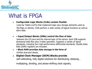
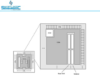
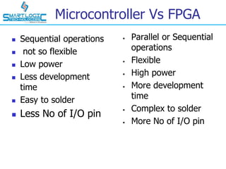
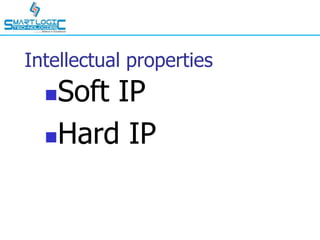
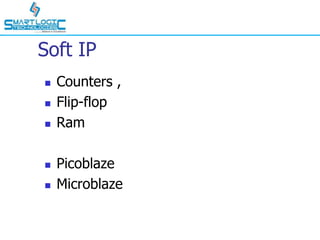
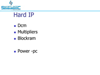
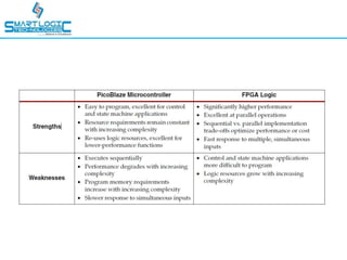
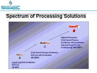
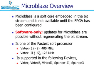


This document provides an overview of processor IP cores in FPGAs. It discusses what an FPGA is and its main components like configurable logic blocks and input/output blocks. It then compares microcontrollers to FPGAs and describes different types of intellectual properties that can be used, including soft IP like counters and hard IP like block RAM. It also discusses using processors like Picoblaze and Microblaze in FPGAs and provides information on their architecture and usage. Finally, it mentions the presenter's contact information for any further questions.