Download as PDF, PPTX


![8/13/2012 Embedded Systems 19
-Contd
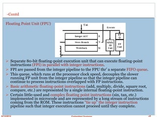
MMX & 3D Unit
Separate execution unit for the MMX-compatible instructions.
One MMX instruction can issue into the MMX unit every clock.
The MMX multiplier is fully pipelined and can start one non-dependent
MMX multiply[-add] instruction (which consists of up to four separate
multiplies) every clock.
Other MMX instructions execute in one clock.
Multiplies followed by a dependent MMX instruction require two clocks.
Separate execution unit for some specific 3D instructions.
These instructions provide assistance for graphics transformations SIMD
(Single Instruction Multiple Data) single-precision floating-point
capabilities.
One 3D instruction can issue into the 3D unit every clock.
The 3D unit has two single-precision floating-point multipliers and two
single-precision floating-point adders. Other functions such as
conversions, reciprocal, and reciprocal square root are provided.
The multiplier and adder are fully pipelined and can start any non-
dependent 3D instructions every clock.](https://image.slidesharecdn.com/ch2embeddedprocessors-i-190410052440/85/Ch2-embedded-processors-i-19-320.jpg)
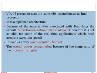
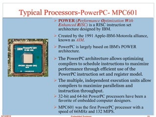


This document discusses embedded processors, including the VIA C3 processor and PowerPC MPC601 processor. It provides details on the architecture and design of the VIA C3 processor, including its instruction pipeline, instruction decode unit, branch prediction, integer unit, floating point unit, MMX and 3D unit. It notes some key characteristics of the VIA C3 such as its use of the x86 instruction set, pipelined design, and higher power consumption due to complexity. The document then briefly introduces the PowerPC MPC601 processor.