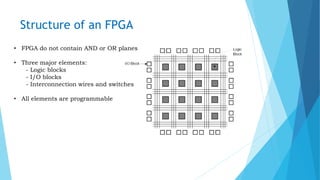
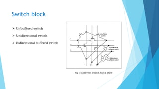
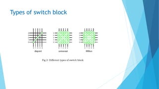
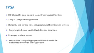
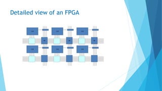
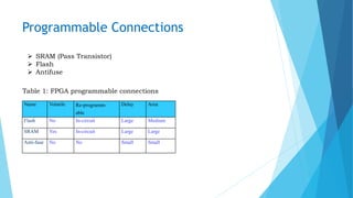
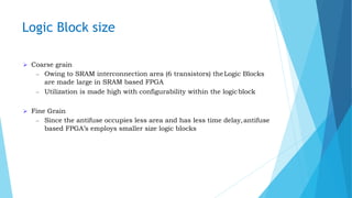
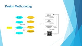
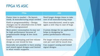
ASIC VS FPGA
Presented by:
Shalini Kamade
Field Programmable Gate Array (FPGA)
 FPGA is a general-purpose integrated circuit that is “programmed” by the
designer rather than the device manufacturer. Unlike an ASIC.
 FPGA can be reprogrammed, even after it has been deployed into a system.
 FPGA programmed by HDL (VHDL or VERILOG)
 Array of logic resources with programmable interconnection.
• Logic resources (Combinational, Flip flops)
• Combinational: LUT, Multiplexers, Gates
• Programmable interconnections: SRAM, Flash, Anti-fuse
• Special Resources: PLL/DLL, RAMs, FIFOs,
• Memory Controllers, Network Interfaces, Processors
FPGA Types and Manufacturers
Two Major Manufacturers (Xilinx and Altera)
 Altera FPGA Families
 Cyclone
 Arria
 Stratix
 Xilinx FPGA Families
 Spartan
 Virtex
 Kintex
 Artix
 Zynq (Soc with ARM Processor)
SPARTAN VERTEX
Structure of an FPGA
• FPGA do not contain AND or OR planes
• Three major elements:
- Logic blocks
- I/O blocks
- Interconnection wires and switches
• All elements are programmable
Switch block
 Unbuffered switch
 Unidirectional switch
 Bidirectional buffered switch
Fig 1: Different switch block style
Types of switch block
Fig 2: Different types of switch block
FPGA
 I/O Blocks (Tri-state output / Input, Synchronizing Flip-flops)
 Array of Configurable Logic Blocks
 Horizontal and Vertical wires with programmable switches in between
 Single length, Double length, Quad, Hex and Long lines
 Resources available to user
 Resources for configuring programmable switches in the
interconnect structures and Logic blocks
Detailed view of an FPGA
Programmable Connections
 SRAM (Pass Transistor)
 Flash
 Antifuse
Name Volatile Re-programm-
able
Delay Area
Flash No In-circuit Large Medium
SRAM Yes In-circuit Large Large
Anti-fuse No No Small Small
Table 1: FPGA programmable connections
Logic Block size
 Coarse grain
– Owing to SRAM interconnection area (6 transistors) theLogic Blocks
are made large in SRAM based FPGA
– Utilization is made high with configurability within the logicblock
 Fine Grain
– Since the antifuse occupies less area and has less time delay,antifuse
based FPGA’s employs smaller size logic blocks
Design Methodology
Commercial Tools
 Simulators
ModelSim (Mentor Graphics)
Active HDL (Aldec)
 Synthesis Tools
Synplify Pro (Synopsys)
Precision Synthesis (Mentor Graphics)
 Vendor Tools
Xilinx ISE (Synthesis, Simulation, PAR, Programming, …)
Xilinx Vivado (Synthesis, Simulation, PAR, Programming, …)
Altera Quartus II (Synthesis, Simulation, PAR, Programming, …)
Cadence Suite
Synopsis Suite
Mentor Graphics Suite
Why replace FPGA by ASIC
 Significant cost reduction.
 Significant power saving.
 Board cost reduction
 No need for Flash/EPROM chip
 Reduce size in a multi – FPGA case
 Eliminates power-up reconfiguration time.
Design Flow Comparison
ASIC Design Flow
FPGA VS ASIC
FPGA ASIC
Faster time to market – No layout,
mask, & manufacturing steps needed
Need longer design times to take
care of all manufacturing steps
Field re-programmability – Design
changes can be absorbed even in field
& FPGA reprogrammed
Once manufactured, need to spin
again a new chip in case of bugs
More power consumption & may not
be high performance because of
programmable design & low clock
speed
Custom design for an application
helps in designing for
power/performance efficiency
Good for prototyping and low volume
design as cost would be less
For larger volume of production,
cost per unit will be much less
Generally not possible to have analog
and mixed signal designs and limited
to what vendor supports
Can support analog and mixed
signal designs
Asic vs fpga

Asic vs fpga

  • 1.
    ASIC VS FPGA Presentedby: Shalini Kamade
  • 2.
    Field Programmable GateArray (FPGA)  FPGA is a general-purpose integrated circuit that is “programmed” by the designer rather than the device manufacturer. Unlike an ASIC.  FPGA can be reprogrammed, even after it has been deployed into a system.  FPGA programmed by HDL (VHDL or VERILOG)  Array of logic resources with programmable interconnection. • Logic resources (Combinational, Flip flops) • Combinational: LUT, Multiplexers, Gates • Programmable interconnections: SRAM, Flash, Anti-fuse • Special Resources: PLL/DLL, RAMs, FIFOs, • Memory Controllers, Network Interfaces, Processors
  • 3.
    FPGA Types andManufacturers Two Major Manufacturers (Xilinx and Altera)  Altera FPGA Families  Cyclone  Arria  Stratix  Xilinx FPGA Families  Spartan  Virtex  Kintex  Artix  Zynq (Soc with ARM Processor)
  • 4.
  • 5.
    Structure of anFPGA • FPGA do not contain AND or OR planes • Three major elements: - Logic blocks - I/O blocks - Interconnection wires and switches • All elements are programmable
  • 6.
    Switch block  Unbufferedswitch  Unidirectional switch  Bidirectional buffered switch Fig 1: Different switch block style
  • 7.
    Types of switchblock Fig 2: Different types of switch block
  • 8.
    FPGA  I/O Blocks(Tri-state output / Input, Synchronizing Flip-flops)  Array of Configurable Logic Blocks  Horizontal and Vertical wires with programmable switches in between  Single length, Double length, Quad, Hex and Long lines  Resources available to user  Resources for configuring programmable switches in the interconnect structures and Logic blocks
  • 9.
  • 10.
    Programmable Connections  SRAM(Pass Transistor)  Flash  Antifuse Name Volatile Re-programm- able Delay Area Flash No In-circuit Large Medium SRAM Yes In-circuit Large Large Anti-fuse No No Small Small Table 1: FPGA programmable connections
  • 11.
    Logic Block size Coarse grain – Owing to SRAM interconnection area (6 transistors) theLogic Blocks are made large in SRAM based FPGA – Utilization is made high with configurability within the logicblock  Fine Grain – Since the antifuse occupies less area and has less time delay,antifuse based FPGA’s employs smaller size logic blocks
  • 12.
  • 13.
    Commercial Tools  Simulators ModelSim(Mentor Graphics) Active HDL (Aldec)  Synthesis Tools Synplify Pro (Synopsys) Precision Synthesis (Mentor Graphics)  Vendor Tools Xilinx ISE (Synthesis, Simulation, PAR, Programming, …) Xilinx Vivado (Synthesis, Simulation, PAR, Programming, …) Altera Quartus II (Synthesis, Simulation, PAR, Programming, …) Cadence Suite Synopsis Suite Mentor Graphics Suite
  • 14.
    Why replace FPGAby ASIC  Significant cost reduction.  Significant power saving.  Board cost reduction  No need for Flash/EPROM chip  Reduce size in a multi – FPGA case  Eliminates power-up reconfiguration time.
  • 15.
  • 16.
  • 17.
    FPGA VS ASIC FPGAASIC Faster time to market – No layout, mask, & manufacturing steps needed Need longer design times to take care of all manufacturing steps Field re-programmability – Design changes can be absorbed even in field & FPGA reprogrammed Once manufactured, need to spin again a new chip in case of bugs More power consumption & may not be high performance because of programmable design & low clock speed Custom design for an application helps in designing for power/performance efficiency Good for prototyping and low volume design as cost would be less For larger volume of production, cost per unit will be much less Generally not possible to have analog and mixed signal designs and limited to what vendor supports Can support analog and mixed signal designs

Editor's Notes

  • #4 Xilinx Spartan-3, Spartan-6 Virtex-4, Virtex-5, Virtex-6, Virtex-7 Artix-7, Kintex-7,, Zynq Altera Cyclone, Cyclone II, Cyclone III, Cyclone IV, Cyclone V (2,3,4,5) Arria II, Arria V Stratix II, Stratix III, Startix IV, Startix V(2,3,4,5)
  • #16 FPGA Tools are generally GUI - driven & push button flow. After the design passes behavioural simulation and STA verification is completed STA is used to verify timing in the design ASIC ASIC tool are generally driven by script Post synthesis STA & equivalency checking must for sign off to foundry Place and route usually done in foundry it require 1 to 3 month(cadence tool used in the foundry) Post-ASIC tools are generally driven by scripts Synthesis static timing analysis and equivalency checking are musts for sign-off to foundry Verification of deep sub-micron effects is required for ASIC
  • #17 1 Day by day technology is increasing and customer also expecting new features like low power, high speed in the device. In this stage the features information is collected by some marketing people . 2 Architecture team will design architecture based on the specification. Architecture is like a block diagram we can find all the details in the design architecture team will estimate the block how much cost, power, and area are required. 3 RTL constructing a digital design using comb & seq circuits. The above architecture is converted into Verilog and VHDL, 4 It is a functional verification of RTL design, we verify the design by applying test cases if verification is failed it will send back to the rtl designing department. 5 it is a process of converting RTL code to gate level netlist. translation optimization mapping 6 Design for testability is a technique which provide facility to test the design after production 7. It is the process of placing blocks in the chip/core area 8. Placement is automatically assigning correct position to the standard cell on the chip without overlapping 9. CLOCK TREE : it is the process of balancing the clock skew. 10 Routing : In this stage we connect all the cells physically with the metal straps. 1) Global Routing : it will tell which signal which metal layer is used 2) Detailed Routing: In detailed routing physical connections are done 11. After the routing physical layout of chip is completed. In sign off stage all the test are done to check the performance of the layout 12. The total design is converted into chip by the manufacturing process. 13.After the fabrication process we test the chip. .