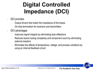
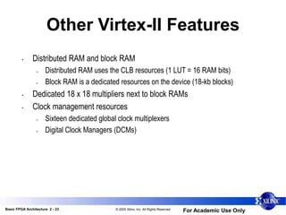
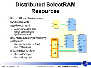
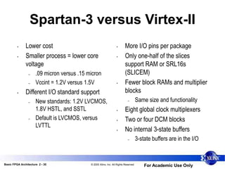
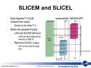
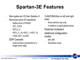
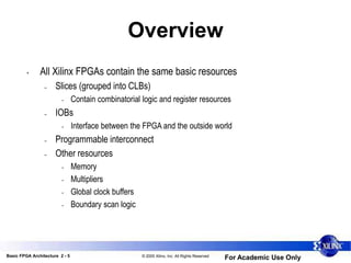
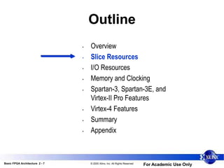
The document outlines the architectural resources and features of Xilinx FPGAs, focusing on the Virtex-II and Virtex-4 families. It details the components such as slices, I/O resources, memory, and clocking resources, along with differences between various FPGA models including Spartan-3 and Spartan-3E. Enhanced features of the newer Virtex-4 devices are also addressed, highlighting advancements in DSP blocks, memory configuration, and global clock management.
![Basic FPGA Architecture 2 - 16 © 2005 Xilinx, Inc. All Rights Reserved
For Academic Use Only
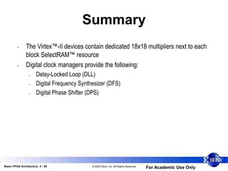
Shift Register LUT
(SRL16CE)
• Dynamically addressable serial
shift registers
– Maximum delay of 16 clock cycles
per LUT (128 per CLB)
– Cascadable to other LUTs or CLBs
for longer shift registers
• Dedicated connection from Q15
to D input of the next SRL16CE
– Shift register length can
be changed
asynchronously
by toggling address A
LUT
D Q
CE
D Q
CE
D Q
CE
D Q
CE
LUT
D
CE
CLK
A[3:0]
Q
Q15 (cascade out)](https://image.slidesharecdn.com/basic-fpga-arch-xilinx-240423045859-1497ac0b/85/Basic-FPGA-Architecture-Virtex-CLB-IO-blocks-14-320.jpg)