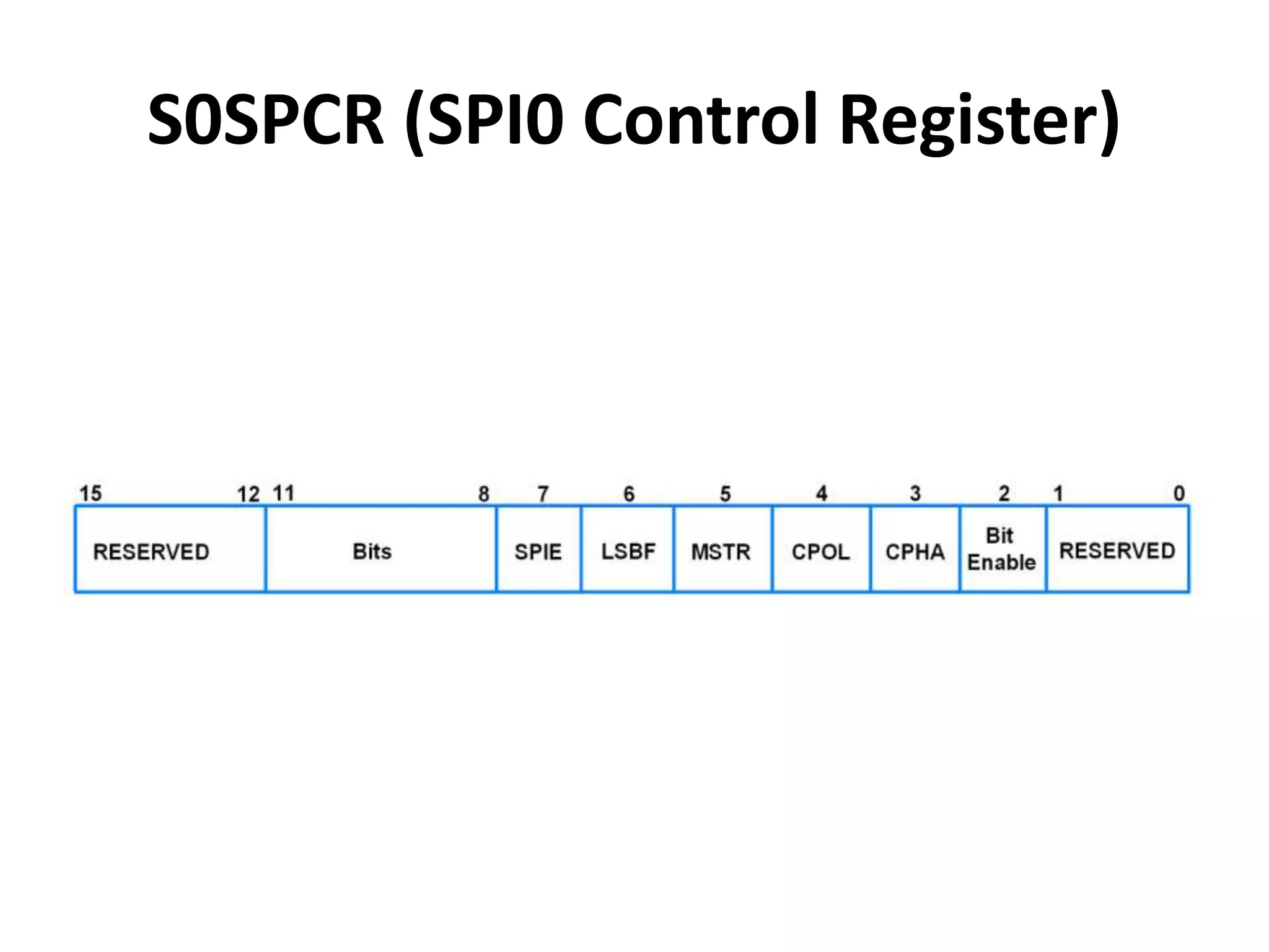
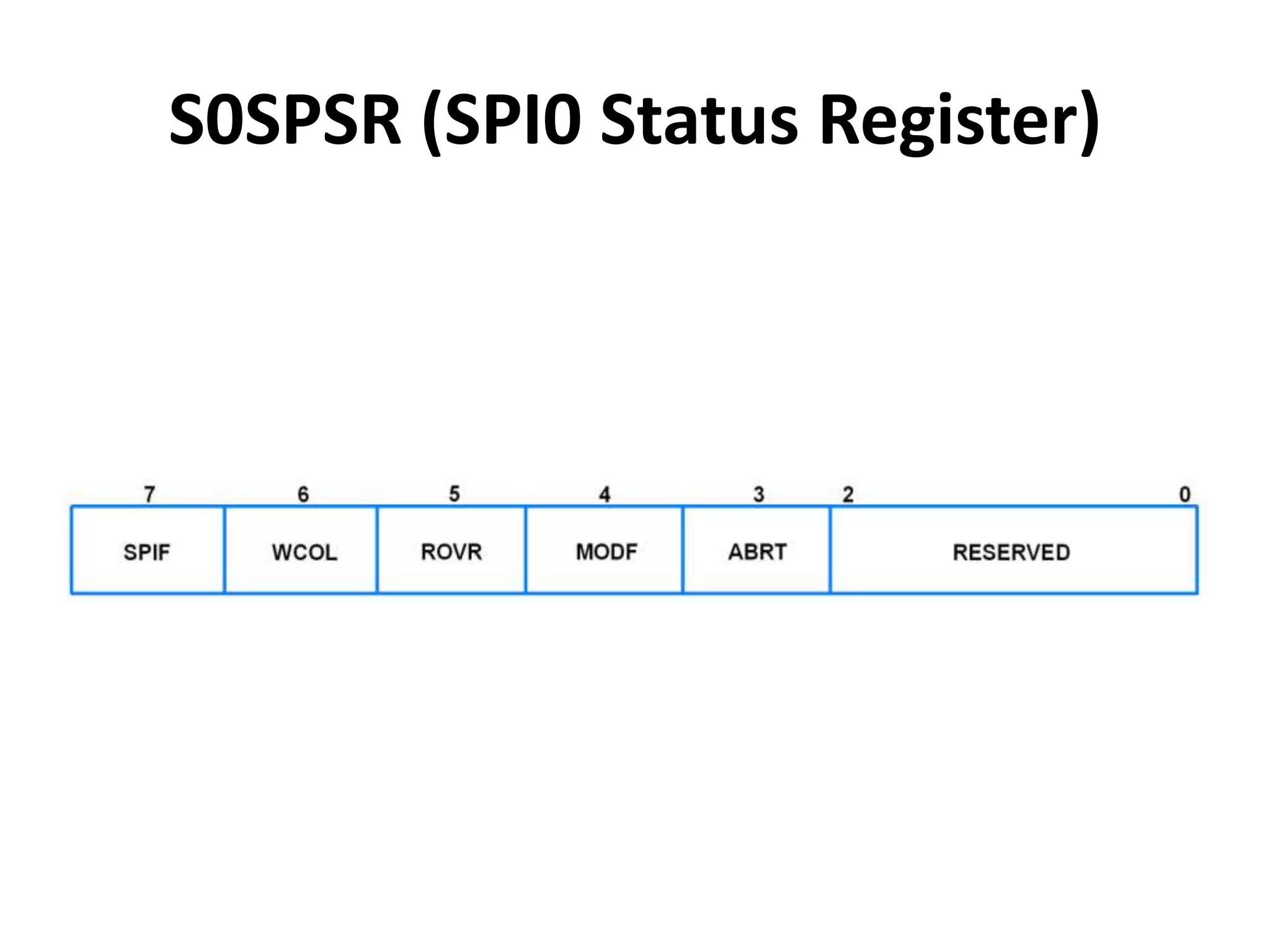
LPC2148 SPI (Serial Peripheral
Interface)
Mrs. D.M.Biradar
Introduction to SPI
• The Serial Peripheral Interface (SPI) is a bus interface connection
protocol originally started by Motorola Corp.
• SPI Interface uses four wires for communication. Hence it is also
known as four wire serial communication protocol.
• SPI is a full duplex master-slave communication protocol. This
means that only a single master and a single slave can communicate
on the interface bus at the same time.
• SPI enabled devices work in two basic modes of SPI operation i.e.
SPI Master Mode and SPI Slave Mode.
• Master Device is responsible for initiation of communication.
• Master Device generates Serial Clock for synchronous data transfer.
• Master Device can handle multiple slave devices on the bus by
selecting them one by one.
S0SPCR (SPI0 Control Register)
• It is a 16-bit register.
• It is a read-write register.
• It is used to control the function of SPI block.
• Bit 2 – Bit Enable
0 = SPI controller sends and receives 8 bits of
data per transfer
1 = SPI controller sends and receives the number
of bits selected by bits 11:8
• Bit 3 – CPHA (Clock Phase)
0 = Data Sampled on Leading Edge of SCK
1 = Data Sampled on Trailing Edge of SCK
• Bit 4 – CPOL (Clock Polarity)
0 = SCK is active high, Leading Edge is Rising
1 = SCK is active low, Leading Edge is Falling
• Bit 5 – MSTR (Master Mode Select)
0 = SPI operates in Slave Mode
1 = SPI operates in Master Mode
• Bit 6 – LSBF (LSB First)
0 = Data transferred MSB (Bit 7) First
1 = Data transferred LSB (Bit 0) First
• Bit 7 – SPIE (Serial Peripheral Interrupt
Enable)
0 = SPI Interrupts are disabled
1 = Hardware interrupt generated each time
SPIF or WCOL bits are activated
• Bit 11:8 – Bits
It decides the number of bits per transfer. Bit2
of this register (Bit Enable) must be 1 for this.
1000 = 8-bits per transfer
1001 = 9-bits per transfer
1010 = 10-bits per transfer
1011 = 11-bits per transfer
1100 = 12-bits per transfer
1101 = 13-bits per transfer
1110 = 14-bits per transfer
1111 = 15-bits per transfer
0000 = 16-bits per transfer
S0SPSR (SPI0 Status Register)
• Bit 3 – ABRT (Slave Abort)
Slave abort happens when slave select pin
goes inactive (high) before data transfer is
complete.
0 = No slave abort
1 = Slave abort occurred
This bit is cleared by reading the register.
• Bit 4 – MODF (Mode Fault)
In SPI Master mode, if SSEL (Slave Select)
signal goes active (low), it means that another
SPI master has selected this device to be
the slave. This condition is known as Mode
fault.
0 = No mode fault
1 = Mode fault occurred
This bit is cleared by reading the register, then
writing to the SPI control register.
• Bit 5 – ROVR (Read Overrun)
When SPI read buffer already contains data to
be read and new data is received before
available data in the buffer is read, then, new
received data will be lost and Read Overrun
bit gets set.
0 = No read overrun
1 = Indicates that a read overrun occurred
This bit is cleared by reading the register.
• Bit 6 – WCOL (Write Collision)
When SPI data transfer is currently in progress
and SPI data register is written with new data
before the current transfer is complete, then,
write collision is said to have occurred and this
bit gets set.
0 = No write collision
1 = Write collision occurred
This bit is cleared by reading the register, then
accessing the SPI data register.
• Bit 7 – SPIF (SPI Transfer Complete Flag)
0 = SPI transfer not completed yet
1 = SPI transfer completed
This bit is cleared by reading the register, then
accessing the SPI data register.
S0SPDR (SPI Data Register)
• This is a 16-bit register.
• It is a read-write register.
• It holds the data to be transmitted/received.
• Once a data transfer starts, writes to this register are
blocked till SPIF becomes 1.
• Bit 7:0 – Data Low
It is lower 8-bit of the data.
• Bit 15:8 – Data High
It is higher 8-bit of the data.
This consists the data bits only when there are more than
8-bits of data per transfer.
The number of data bits per transfer is decided by the bits
11:8 in the SPI0 control register.
LPC2148 SPI (Serial Peripheral Interface).pptx

LPC2148 SPI (Serial Peripheral Interface).pptx

  • 1.
    LPC2148 SPI (SerialPeripheral Interface) Mrs. D.M.Biradar
  • 2.
    Introduction to SPI •The Serial Peripheral Interface (SPI) is a bus interface connection protocol originally started by Motorola Corp. • SPI Interface uses four wires for communication. Hence it is also known as four wire serial communication protocol. • SPI is a full duplex master-slave communication protocol. This means that only a single master and a single slave can communicate on the interface bus at the same time. • SPI enabled devices work in two basic modes of SPI operation i.e. SPI Master Mode and SPI Slave Mode. • Master Device is responsible for initiation of communication. • Master Device generates Serial Clock for synchronous data transfer. • Master Device can handle multiple slave devices on the bus by selecting them one by one.
  • 3.
  • 4.
    • It isa 16-bit register. • It is a read-write register. • It is used to control the function of SPI block. • Bit 2 – Bit Enable 0 = SPI controller sends and receives 8 bits of data per transfer 1 = SPI controller sends and receives the number of bits selected by bits 11:8 • Bit 3 – CPHA (Clock Phase) 0 = Data Sampled on Leading Edge of SCK 1 = Data Sampled on Trailing Edge of SCK
  • 5.
    • Bit 4– CPOL (Clock Polarity) 0 = SCK is active high, Leading Edge is Rising 1 = SCK is active low, Leading Edge is Falling • Bit 5 – MSTR (Master Mode Select) 0 = SPI operates in Slave Mode 1 = SPI operates in Master Mode • Bit 6 – LSBF (LSB First) 0 = Data transferred MSB (Bit 7) First 1 = Data transferred LSB (Bit 0) First
  • 6.
    • Bit 7– SPIE (Serial Peripheral Interrupt Enable) 0 = SPI Interrupts are disabled 1 = Hardware interrupt generated each time SPIF or WCOL bits are activated
  • 7.
    • Bit 11:8– Bits It decides the number of bits per transfer. Bit2 of this register (Bit Enable) must be 1 for this. 1000 = 8-bits per transfer 1001 = 9-bits per transfer 1010 = 10-bits per transfer 1011 = 11-bits per transfer 1100 = 12-bits per transfer 1101 = 13-bits per transfer 1110 = 14-bits per transfer 1111 = 15-bits per transfer 0000 = 16-bits per transfer
  • 8.
  • 9.
    • Bit 3– ABRT (Slave Abort) Slave abort happens when slave select pin goes inactive (high) before data transfer is complete. 0 = No slave abort 1 = Slave abort occurred This bit is cleared by reading the register.
  • 10.
    • Bit 4– MODF (Mode Fault) In SPI Master mode, if SSEL (Slave Select) signal goes active (low), it means that another SPI master has selected this device to be the slave. This condition is known as Mode fault. 0 = No mode fault 1 = Mode fault occurred This bit is cleared by reading the register, then writing to the SPI control register.
  • 11.
    • Bit 5– ROVR (Read Overrun) When SPI read buffer already contains data to be read and new data is received before available data in the buffer is read, then, new received data will be lost and Read Overrun bit gets set. 0 = No read overrun 1 = Indicates that a read overrun occurred This bit is cleared by reading the register.
  • 12.
    • Bit 6– WCOL (Write Collision) When SPI data transfer is currently in progress and SPI data register is written with new data before the current transfer is complete, then, write collision is said to have occurred and this bit gets set. 0 = No write collision 1 = Write collision occurred This bit is cleared by reading the register, then accessing the SPI data register.
  • 13.
    • Bit 7– SPIF (SPI Transfer Complete Flag) 0 = SPI transfer not completed yet 1 = SPI transfer completed This bit is cleared by reading the register, then accessing the SPI data register.
  • 14.
    S0SPDR (SPI DataRegister) • This is a 16-bit register. • It is a read-write register. • It holds the data to be transmitted/received. • Once a data transfer starts, writes to this register are blocked till SPIF becomes 1. • Bit 7:0 – Data Low It is lower 8-bit of the data. • Bit 15:8 – Data High It is higher 8-bit of the data. This consists the data bits only when there are more than 8-bits of data per transfer. The number of data bits per transfer is decided by the bits 11:8 in the SPI0 control register.