This document discusses basic semiconductor theory, including:
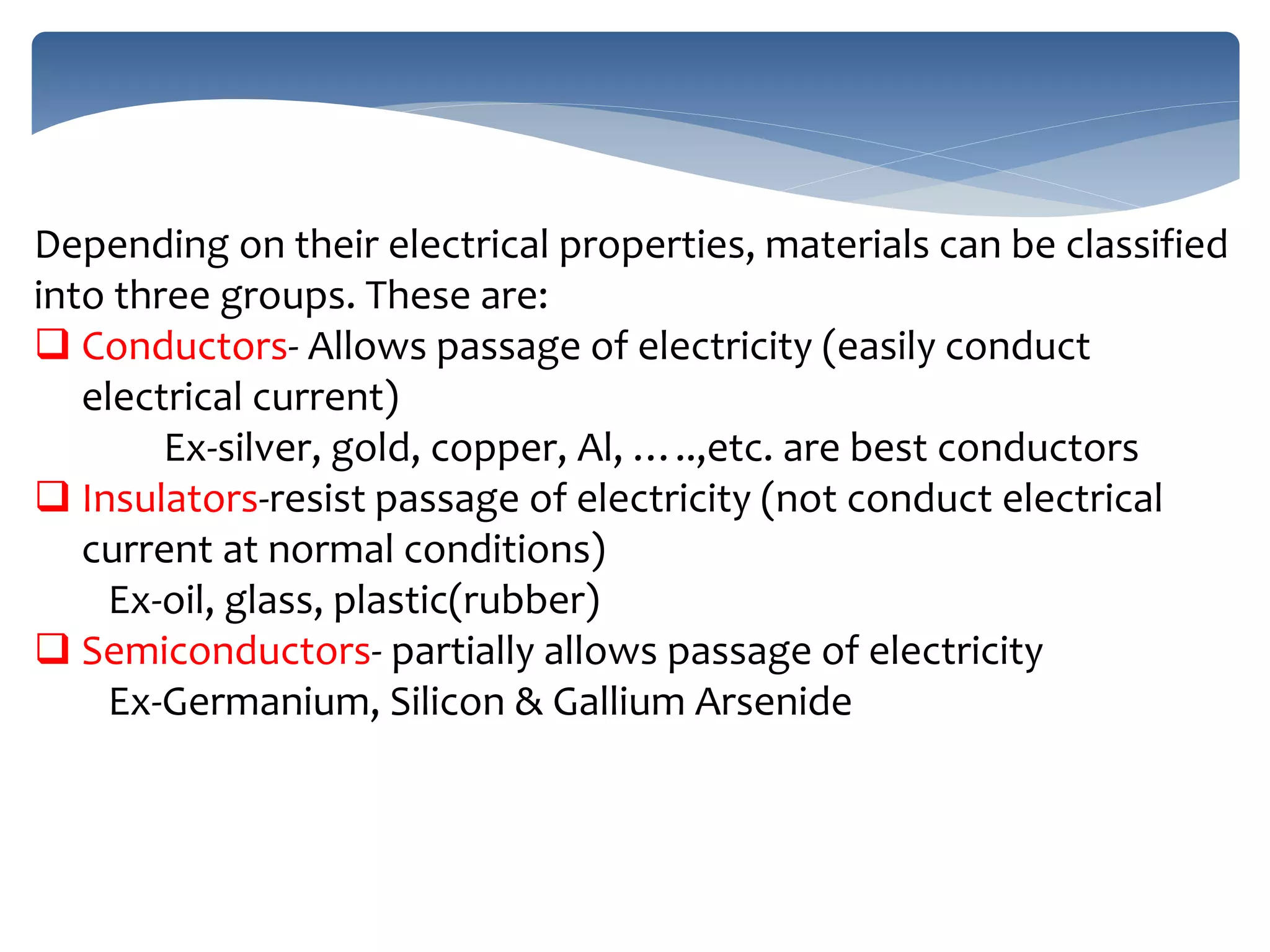
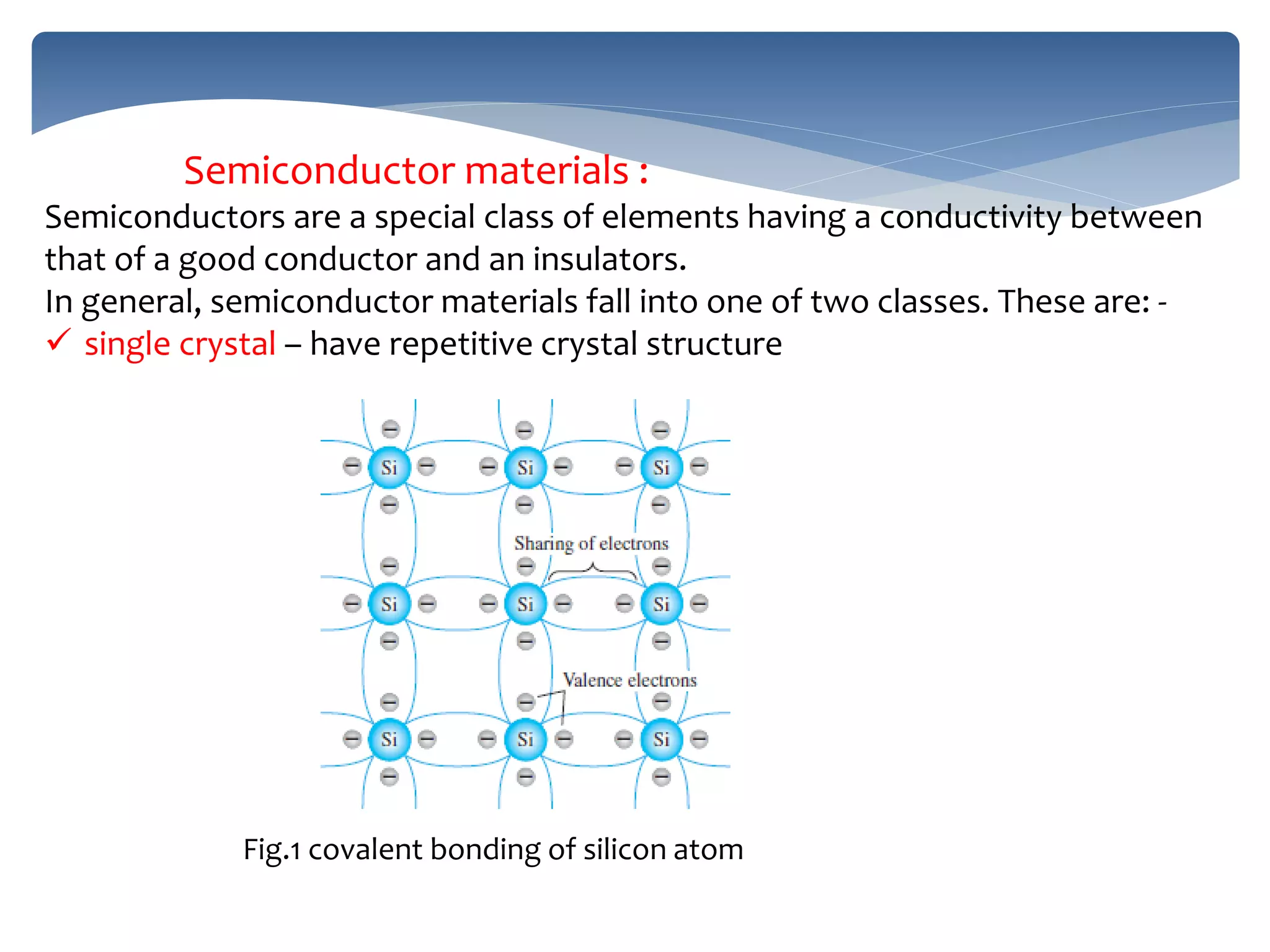
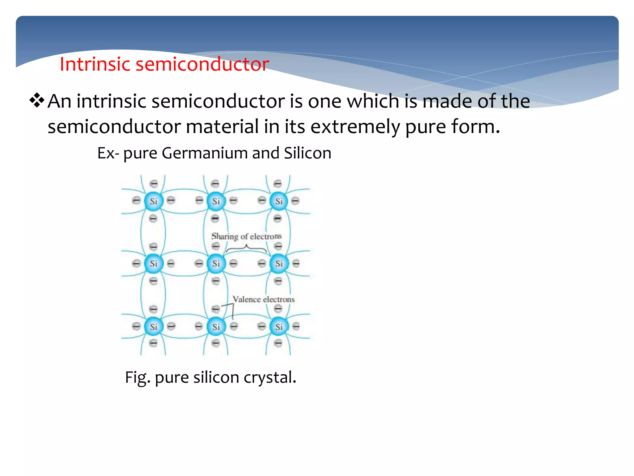
1. Semiconductors have conductivity between conductors and insulators and include materials like silicon, germanium, and gallium arsenide.
2. Doping semiconductors with impurities creates n-type or p-type materials by introducing excess electrons or holes.
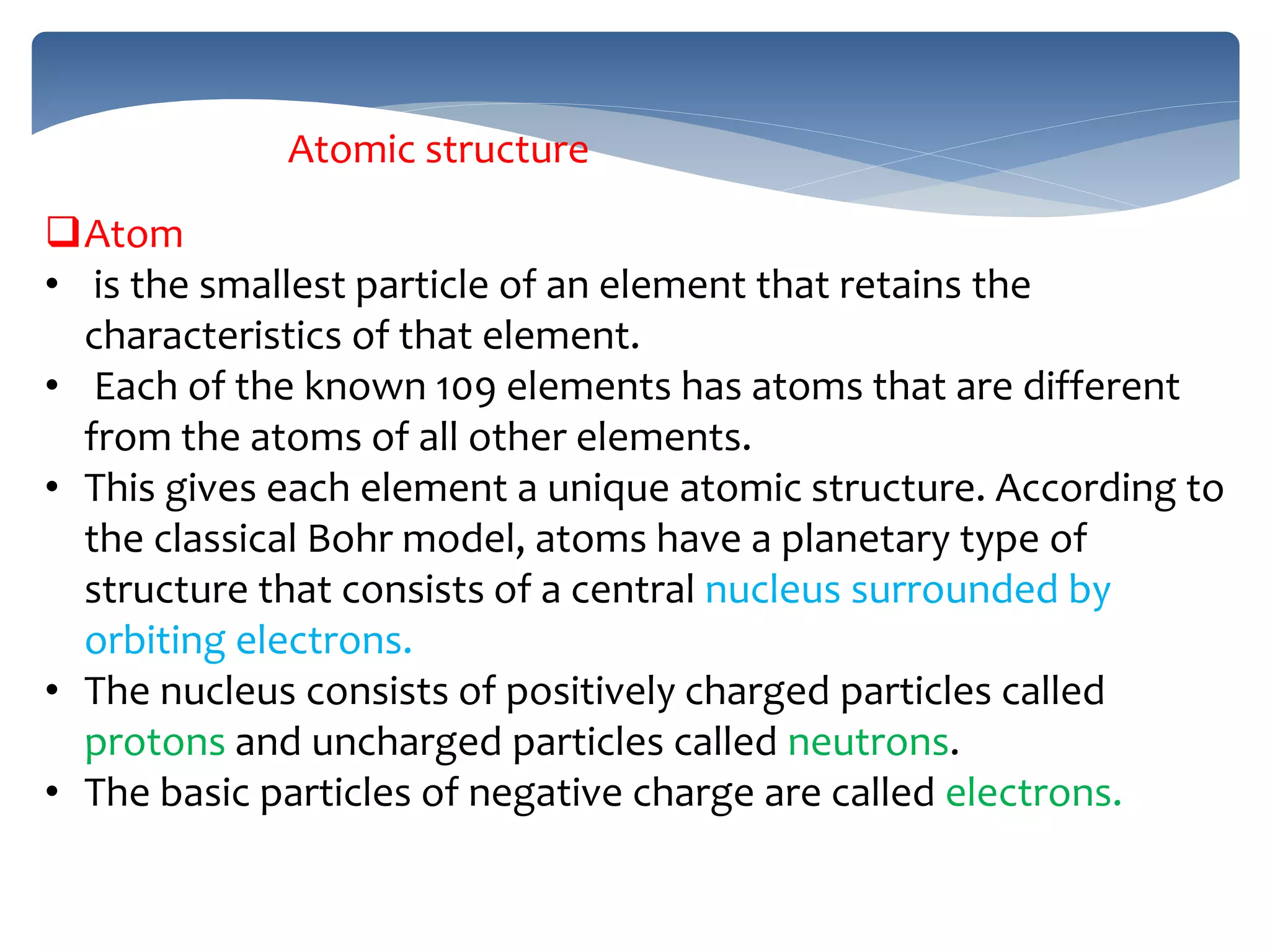
3. The atomic structure of semiconductors includes valence and conduction energy bands separated by a bandgap through which electrons can jump with sufficient energy.
Introduction to Semiconductor Devices.
In modern world no other technology permeates every nook and cranny of our existence as does electronics.
Application of electronics are : Televisions, radios, stereo equipment, computers, scanners, electronic control systems (in cars for example) etc.
First op amps built in 1930’s-1940’s
Technically feedback amplifiers due to only having one useable input
Used in WW-II to help how to strike military targets
Buffers, summers, differentiators, inverters
Took ±300V to ± 100V to power
Pn junction diode by sarmad baloch
I AM SARMAD KHOSA
BSIT (5TH A)
(ISP)
FACEBOOK PAGLE::
https://www.facebook.com/LAUGHINGHLAUGHTER/
YOUTUBE CHANNEL:::
https://www.youtube.com/channel/UCUjaIeS-DHI9xv-ZnBpx2hQ
This ppt is about semiconductor diodes.You can get every basic information about PN junction diode and its working and some more information about the semiconductors.
The three terminals of the FET are known as Gate, Drain, and Source.
It is a voltage controlled device, where the input voltage controls by the output current.
In FET current used to flow between the drain and the source terminal. And this current can be controlled by applying the voltage between the gate and the source terminal.
So this applied voltage generate the electric field within the device and by controlling these electric field we can control the flow of current through the device.
Explore the innovative world of trenchless pipe repair with our comprehensive guide, "The Benefits and Techniques of Trenchless Pipe Repair." This document delves into the modern methods of repairing underground pipes without the need for extensive excavation, highlighting the numerous advantages and the latest techniques used in the industry.
Learn about the cost savings, reduced environmental impact, and minimal disruption associated with trenchless technology. Discover detailed explanations of popular techniques such as pipe bursting, cured-in-place pipe (CIPP) lining, and directional drilling. Understand how these methods can be applied to various types of infrastructure, from residential plumbing to large-scale municipal systems.
Ideal for homeowners, contractors, engineers, and anyone interested in modern plumbing solutions, this guide provides valuable insights into why trenchless pipe repair is becoming the preferred choice for pipe rehabilitation. Stay informed about the latest advancements and best practices in the field.
Saudi Arabia stands as a titan in the global energy landscape, renowned for its abundant oil and gas resources. It's the largest exporter of petroleum and holds some of the world's most significant reserves. Let's delve into the top 10 oil and gas projects shaping Saudi Arabia's energy future in 2024.
TECHNICAL TRAINING MANUAL GENERAL FAMILIARIZATION COURSEDuvanRamosGarzon1
AIRCRAFT GENERAL
The Single Aisle is the most advanced family aircraft in service today, with fly-by-wire flight controls.
The A318, A319, A320 and A321 are twin-engine subsonic medium range aircraft.
The family offers a choice of engines
COLLEGE BUS MANAGEMENT SYSTEM PROJECT REPORT.pdfKamal Acharya
The College Bus Management system is completely developed by Visual Basic .NET Version. The application is connect with most secured database language MS SQL Server. The application is develop by using best combination of front-end and back-end languages. The application is totally design like flat user interface. This flat user interface is more attractive user interface in 2017. The application is gives more important to the system functionality. The application is to manage the student’s details, driver’s details, bus details, bus route details, bus fees details and more. The application has only one unit for admin. The admin can manage the entire application. The admin can login into the application by using username and password of the admin. The application is develop for big and small colleges. It is more user friendly for non-computer person. Even they can easily learn how to manage the application within hours. The application is more secure by the admin. The system will give an effective output for the VB.Net and SQL Server given as input to the system. The compiled java program given as input to the system, after scanning the program will generate different reports. The application generates the report for users. The admin can view and download the report of the data. The application deliver the excel format reports. Because, excel formatted reports is very easy to understand the income and expense of the college bus. This application is mainly develop for windows operating system users. In 2017, 73% of people enterprises are using windows operating system. So the application will easily install for all the windows operating system users. The application-developed size is very low. The application consumes very low space in disk. Therefore, the user can allocate very minimum local disk space for this application.
Hybrid optimization of pumped hydro system and solar- Engr. Abdul-Azeez.pdffxintegritypublishin
Advancements in technology unveil a myriad of electrical and electronic breakthroughs geared towards efficiently harnessing limited resources to meet human energy demands. The optimization of hybrid solar PV panels and pumped hydro energy supply systems plays a pivotal role in utilizing natural resources effectively. This initiative not only benefits humanity but also fosters environmental sustainability. The study investigated the design optimization of these hybrid systems, focusing on understanding solar radiation patterns, identifying geographical influences on solar radiation, formulating a mathematical model for system optimization, and determining the optimal configuration of PV panels and pumped hydro storage. Through a comparative analysis approach and eight weeks of data collection, the study addressed key research questions related to solar radiation patterns and optimal system design. The findings highlighted regions with heightened solar radiation levels, showcasing substantial potential for power generation and emphasizing the system's efficiency. Optimizing system design significantly boosted power generation, promoted renewable energy utilization, and enhanced energy storage capacity. The study underscored the benefits of optimizing hybrid solar PV panels and pumped hydro energy supply systems for sustainable energy usage. Optimizing the design of solar PV panels and pumped hydro energy supply systems as examined across diverse climatic conditions in a developing country, not only enhances power generation but also improves the integration of renewable energy sources and boosts energy storage capacities, particularly beneficial for less economically prosperous regions. Additionally, the study provides valuable insights for advancing energy research in economically viable areas. Recommendations included conducting site-specific assessments, utilizing advanced modeling tools, implementing regular maintenance protocols, and enhancing communication among system components.
Vaccine management system project report documentation..pdfKamal Acharya
The Division of Vaccine and Immunization is facing increasing difficulty monitoring vaccines and other commodities distribution once they have been distributed from the national stores. With the introduction of new vaccines, more challenges have been anticipated with this additions posing serious threat to the already over strained vaccine supply chain system in Kenya.
Quality defects in TMT Bars, Possible causes and Potential Solutions.PrashantGoswami42
Maintaining high-quality standards in the production of TMT bars is crucial for ensuring structural integrity in construction. Addressing common defects through careful monitoring, standardized processes, and advanced technology can significantly improve the quality of TMT bars. Continuous training and adherence to quality control measures will also play a pivotal role in minimizing these defects.
CFD Simulation of By-pass Flow in a HRSG module by R&R Consult.pptxR&R Consult
CFD analysis is incredibly effective at solving mysteries and improving the performance of complex systems!
Here's a great example: At a large natural gas-fired power plant, where they use waste heat to generate steam and energy, they were puzzled that their boiler wasn't producing as much steam as expected.
R&R and Tetra Engineering Group Inc. were asked to solve the issue with reduced steam production.
An inspection had shown that a significant amount of hot flue gas was bypassing the boiler tubes, where the heat was supposed to be transferred.
R&R Consult conducted a CFD analysis, which revealed that 6.3% of the flue gas was bypassing the boiler tubes without transferring heat. The analysis also showed that the flue gas was instead being directed along the sides of the boiler and between the modules that were supposed to capture the heat. This was the cause of the reduced performance.
Based on our results, Tetra Engineering installed covering plates to reduce the bypass flow. This improved the boiler's performance and increased electricity production.
It is always satisfying when we can help solve complex challenges like this. Do your systems also need a check-up or optimization? Give us a call!
Work done in cooperation with James Malloy and David Moelling from Tetra Engineering.
More examples of our work https://www.r-r-consult.dk/en/cases-en/
Automobile Management System Project Report.pdfKamal Acharya
The proposed project is developed to manage the automobile in the automobile dealer company. The main module in this project is login, automobile management, customer management, sales, complaints and reports. The first module is the login. The automobile showroom owner should login to the project for usage. The username and password are verified and if it is correct, next form opens. If the username and password are not correct, it shows the error message.
When a customer search for a automobile, if the automobile is available, they will be taken to a page that shows the details of the automobile including automobile name, automobile ID, quantity, price etc. “Automobile Management System” is useful for maintaining automobiles, customers effectively and hence helps for establishing good relation between customer and automobile organization. It contains various customized modules for effectively maintaining automobiles and stock information accurately and safely.
When the automobile is sold to the customer, stock will be reduced automatically. When a new purchase is made, stock will be increased automatically. While selecting automobiles for sale, the proposed software will automatically check for total number of available stock of that particular item, if the total stock of that particular item is less than 5, software will notify the user to purchase the particular item.
Also when the user tries to sale items which are not in stock, the system will prompt the user that the stock is not enough. Customers of this system can search for a automobile; can purchase a automobile easily by selecting fast. On the other hand the stock of automobiles can be maintained perfectly by the automobile shop manager overcoming the drawbacks of existing system.
Cosmetic shop management system project report.pdfKamal Acharya
Buying new cosmetic products is difficult. It can even be scary for those who have sensitive skin and are prone to skin trouble. The information needed to alleviate this problem is on the back of each product, but it's thought to interpret those ingredient lists unless you have a background in chemistry.
Instead of buying and hoping for the best, we can use data science to help us predict which products may be good fits for us. It includes various function programs to do the above mentioned tasks.
Data file handling has been effectively used in the program.
The automated cosmetic shop management system should deal with the automation of general workflow and administration process of the shop. The main processes of the system focus on customer's request where the system is able to search the most appropriate products and deliver it to the customers. It should help the employees to quickly identify the list of cosmetic product that have reached the minimum quantity and also keep a track of expired date for each cosmetic product. It should help the employees to find the rack number in which the product is placed.It is also Faster and more efficient way.
NO1 Uk best vashikaran specialist in delhi vashikaran baba near me online vas...Amil Baba Dawood bangali
Contact with Dawood Bhai Just call on +92322-6382012 and we'll help you. We'll solve all your problems within 12 to 24 hours and with 101% guarantee and with astrology systematic. If you want to take any personal or professional advice then also you can call us on +92322-6382012 , ONLINE LOVE PROBLEM & Other all types of Daily Life Problem's.Then CALL or WHATSAPP us on +92322-6382012 and Get all these problems solutions here by Amil Baba DAWOOD BANGALI
#vashikaranspecialist #astrologer #palmistry #amliyaat #taweez #manpasandshadi #horoscope #spiritual #lovelife #lovespell #marriagespell#aamilbabainpakistan #amilbabainkarachi #powerfullblackmagicspell #kalajadumantarspecialist #realamilbaba #AmilbabainPakistan #astrologerincanada #astrologerindubai #lovespellsmaster #kalajaduspecialist #lovespellsthatwork #aamilbabainlahore#blackmagicformarriage #aamilbaba #kalajadu #kalailam #taweez #wazifaexpert #jadumantar #vashikaranspecialist #astrologer #palmistry #amliyaat #taweez #manpasandshadi #horoscope #spiritual #lovelife #lovespell #marriagespell#aamilbabainpakistan #amilbabainkarachi #powerfullblackmagicspell #kalajadumantarspecialist #realamilbaba #AmilbabainPakistan #astrologerincanada #astrologerindubai #lovespellsmaster #kalajaduspecialist #lovespellsthatwork #aamilbabainlahore #blackmagicforlove #blackmagicformarriage #aamilbaba #kalajadu #kalailam #taweez #wazifaexpert #jadumantar #vashikaranspecialist #astrologer #palmistry #amliyaat #taweez #manpasandshadi #horoscope #spiritual #lovelife #lovespell #marriagespell#aamilbabainpakistan #amilbabainkarachi #powerfullblackmagicspell #kalajadumantarspecialist #realamilbaba #AmilbabainPakistan #astrologerincanada #astrologerindubai #lovespellsmaster #kalajaduspecialist #lovespellsthatwork #aamilbabainlahore #Amilbabainuk #amilbabainspain #amilbabaindubai #Amilbabainnorway #amilbabainkrachi #amilbabainlahore #amilbabaingujranwalan #amilbabainislamabad
2. Depending on their electrical properties, materials can be classified
into three groups. These are:
Conductors- Allows passage of electricity (easily conduct
electrical current)
Ex-silver, gold, copper, Al, …..,etc. are best conductors
Insulators-resist passage of electricity (not conduct electrical
current at normal conditions)
Ex-oil, glass, plastic(rubber)
Semiconductors- partially allows passage of electricity
Ex-Germanium, Silicon & Gallium Arsenide
3. Semiconductor materials :
Semiconductors are a special class of elements having a conductivity between
that of a good conductor and an insulators.
In general, semiconductor materials fall into one of two classes. These are: -
single crystal – have repetitive crystal structure
Fig.1 covalent bonding of silicon atom
4. compound crystals- constructed of two or more semiconductor
materials of different atomic structure.
Fig.2 covalent bonding of GaAs crystal
5. For the discovery of the diode and transistors germanium was
used exclusively. Because of
1. Relatively easy to find
2. Available in large quantity
3. Easy to refine (to obtain in very high level of purity)
Disadvantage of using Germanium
1. Heavy leakage current (sensitive to change in temperature)
2. Fabrication of germanium wafer is complex.
6. Silicon – is a semiconductor material of choice. Because of:
1. It improved temperature sensitivity(decreased leakage current)
2. Most abundant material on earth
3. Easy to design
4. Easily fabricated
Disadvantage of using silicon
Its refining process for manufacturing silicon of very high level of purity is
difficult.
Gallium arsenide
For the issue of speed for computers and communication systems gallium
arsenide is preferable one. Speed of GaAs=5*silicon
Draw back of using gallium arsenide
1. Difficult to manufacture at high level of purity
2. More expensive
7. Atomic structure
Atom
• is the smallest particle of an element that retains the
characteristics of that element.
• Each of the known 109 elements has atoms that are different
from the atoms of all other elements.
• This gives each element a unique atomic structure. According to
the classical Bohr model, atoms have a planetary type of
structure that consists of a central nucleus surrounded by
orbiting electrons.
• The nucleus consists of positively charged particles called
protons and uncharged particles called neutrons.
• The basic particles of negative charge are called electrons.
8. • Therefore, Fundamental components of an atom are electron,
proton and neutron.
• Protons and neutrons form the nucleus and electrons appear in
fixed orbit around the nucleus.
• atom is electrically neutral.
• Number of electrons and protons are equal.
Continued
9. ion
- Is an atom that gain or loose an electron.
(+ve ion-when atom loose electron & -ve ion when it gain electron)
-If a valence electron acquires a sufficient amount of energy, it
can actually escape from the outer shell and the atom's influence.
-The departure of a valence electron leaves a previously neutral
atom with an excess of positive charge (more protons than
electrons).
-The process of losing a valence electron is known as ionization.
and the resulting positively charged atom is called a positive ion.
Ionization energy-
energy required by an electron to come out of the atom and
the material completely.
11. Covalent bonding and intrinsic materials
covalent bonding
is a bonding of atoms strengthened by sharing of electrons.
when external energy (light energy or heat energy) is
applied, the bond breaks and electrons are released
from the bond.
The hole or free electron is said to be created.
Free electron
is an electron do not bonded but within the medium.
Hole
is absence of an electron (vacant site).
12. An increase in temperature of semiconductor can result in a
substantial increase in the number of free electrons in the
material.
Semiconductor materials have a negative temperature
coefficient.
↑temp =↑in number of free carrier. (but, reverse for conductors)
= ↓in resistance of semiconductor.
13. Energy band
the electrons of an atom can exist only within prescribed
energy bands.
Each shell around the nucleus corresponds to a certain energy
band and is separated from adjacent shells by energy gaps, in
which no electrons can exist. Figure below shows the energy
band diagram for an unexcited (no external energy such as
heat) atom in a pure silicon crystal.
This condition occurs only at a temperature of absolute 0
Kelvin.
14. Fig4. Energy band diagram for an unexcited atom in a pure (intrinsic) silicon crystal.
There are no electrons in the conduction band.
16. o Valence electrons
The outer most electrons of an atom and have least binding
energy.
o Valence band
The band of energy occupied by the valence electrons.
It may be completely filled or partially filled with electrons but
never empty.
o Conduction band
The higher permitted energy band.
May either be empty or partially filled with electrons.
o Conduction electrons
Are electrons can move freely in the conduction band.
o Forbidden energy gap(Eg)
The gap between valence band and conduction band.
17. If valence electron happen to absorb enough energy, it jumps
across the forbidden energy gap and enters the conduction
band.
When an electron is ejected from the valence band, hole is left
behind.
Conduction band has nothing to do with hole flow.
Hole flow experiences more opposition than electron flow in
the conduction band.
18. Energy bands of materials
Fig6. Energy diagrams for the three types of materials.
19. Insulators
Their valence electrons bound very tightly to their parent atoms.
No free charge carriers available within them under normal condition.
Full valence bands.
Empty conduction bands.
Large energy gap (Eg).
At ordinary temperature, the probability of electrons to cross the band gap
is slight.
Conductors
There is no physical distinction between the two bands.
(VB & CB overlaps).
There is no structure to establish holes.
The total current in such conductors is simply a flow of electrons.
20. Semiconductors
At normal condition, empty conduction band and almost filled
valence band with a very narrow energy gap(Eg).
With increase in temperature, width of energy gap decreases
and some of the electrons are liberated into the conduction
band.
22. Intrinsic semiconductor
An intrinsic semiconductor is one which is made of the
semiconductor material in its extremely pure form.
Ex- pure Germanium and Silicon
Fig. pure silicon crystal.
23. Process of adding impurities to a pure semiconductor is called
doping.
A semiconductor material that has been subjected to the
doping process is called an extrinsic material.
Conducting property of intrinsic semiconductors can be
improved in the following ways.
1. By changing the temperature of the environment.
2. By illumination of medium-(light energy)
3. By applying magnetic field-(magnetic energy)
4. By addition of impurities.
24. N-type extrinsic semiconductor
An N-type semiconductor is obtained when a pentavalent atom
like Antimony, Arsenic and Phosphorus are added to pure
Germanium or silicon crystals.
Diffused impurities with five valence electrons are called donor
atoms.
Fig. Diffused donor atom(Sb) to pure silicon crystal.
25. Concentration of electrons in conduction band, exceeds the
concentration of holes in the valence band.
Fig. Concentration of donor ions in N-type semiconductor.
In an n-type material the electron is called the majority
carrier and the hole is minority carrier.
26. P-type material
The p-type material is formed by doping a pure Germanium or
silicon crystal with trivalent atoms like Boron, Gallium and
Indium.
Fig. Diffused acceptor atom(B) to pure silicon crystal.
27. The three valence electrons of Boron atom form covalent
bonds with four surrounding silicon atom but , one bond is left
incomplete and give rise to a hole.
The diffused impurities with three valence electrons are called
acceptor atoms.
Concentration of holes in valence band, exceeds the
concentration of electrons in the conduction band.
In a p-type material the hole is majority carrier and electron is
the minority carrier.
Fig. Concentration of donor ions in N-type semiconductor.