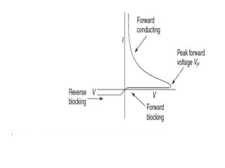
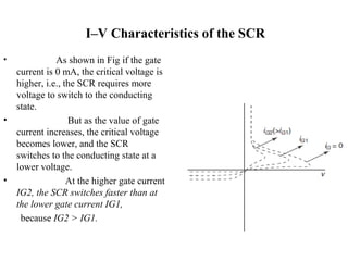
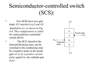
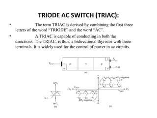
Objectives:
Power electronic Devices play a major role
in modern electronic design. High-power
semiconductor devices have better switching
speed, they are smaller in size and cost of
production is also low.
Subsequently, the
SCR,TRIAC, DIAC, UJT and IGBT are
discussed in a similar manner with respect to
their real life application.
Power Semiconductor Switches
Power Diodes Power Transistors Thyristors
2 layer device 3 layer Device 4 layer
Device
• Thyristor devices can convert and control large amounts of power in AC or
DC systems while using very low power for control.
• Thyristor family includes
1- Silicon controlled switch (SCR)
2- Gate-turnoff thyristor (GTO)
3- Triac
4- Diac
5- Silicon controlled switch (SCS)
6- Mos-controlled switch (MCT)
2
INTRODUCTION:
The SCR is the most important special semiconductor
device. This device is popular for its Forward-Conducting
and Reverse-blocking characteristics.
SCR can be used in high-power devices. For
example, in the central processing unit of the computer, the
SCR is used in switch mode power supply (SMPS).
The DIAC, a combination of two Shockley
Diodes, and the TRIAC, a combination of two SCRs
connected
anti-parallelly are important power-control devices. The
UJT is also used as an efficient switching device.
SILICON-CONTROLLED RECTIFIER
(SCR)
The silicon-controlled rectifier or
semiconductor controlled rectifier is a two-state
device used for efficient power control.
SCR is the parent member of the thyristor
family and is used in high-power electronics.Its
constructional features, physical operation and
characteristics are explained in the following
sections.
Constructional Features
The SCR is a four-layer structure, either
p–n–p–n or n–p–n–p, that effectively blocks current
through two terminals until it is turned ON by a small-
signal at a third terminal.
The SCR has two states: a high-current
low-impedance ON state and a low-current high-
impedance OFF state.
The basic transistor action in a four-layer
p–n–p–n structure is analysed first with only two
terminals,and then the third control input is introduced.
Physical Operation and
Characteristics
• The physical operation of the SCR can be
explained clearly with reference to the current–voltage
characteristics.
• The forward-bias condition and reverse-bias
condition illustrate the conducting state and the
reverse blocking state respectively. Based on these
two states a typical I –V characteristic of the SCR is
shown
SCR in Forward Bias:
• There are two different states in which we can examine the
SCR in the forward-biased condition:
(i) The high- impedance or forward-blocking state
(ii) The low-impedance or forward-conducting state
At a critical peak forward voltage Vp, the SCR switches from the
blocking state to the conducting state
• A positive voltage places junction j1 and j3 under
forward-bias, and the centre junction j2 under reverse-bias.
• The for ward voltage in the blocking state appears across
the reverse-biased junction j2 as the applied voltage V is
increased. The voltage from the anode A to cathode C, is very
small after switching to the forward-conducting state, and all three
junctions are forward-biased. The junction j2 switches from
reverse-bias to forward-bias..
SCR in Reverse Bias:
 In the reverse-blocking state the junctions j1 and j3 are reverse-
biased, and j2 is forward-biased.
 The supply of electrons and holes to junction j2 is restricted, and
due to the thermal generation of electron–hole pairs near junctions j1 and j2
the device current is a small saturation current.
 In the reverse blocking condition the current remains small until
avalanche breakdown occurs at a large reverse-bias of several thousand volts.
 An SCR p–n–p–n structure is equivalent to one p–n–p transistor
and one n–p–n transistor sharing some common terminals.
 Collector current I C1 = α1i + I CO1 having a transfer ratio α 1 for the p–n–p.
 Collector current I C2 =α2i + I CO2 having a transfer ratio a2 for the n–p–n.
 ICO1 and ICO2 stand for the respective collector-saturation currents.
I C1 = α 1i + I CO1 = I B2 ……………….
I C2 = α 2 i + I CO2 = I B1 ………………
SCR in Reverse Bias
• The total current through the SCR is the sum of iC1 and iC2:
• I C1 + I = i ………………..(8-3)
• Substituting the values of collector current from Eqs. (8-1) and (8-2) in Eq. (8-3) we
get:
• i (α1 + α2) + I CO1 + I CO2 = i
• i = (I CO1 + I CO2 ) /(1- α1 + α2) ………………..(8-4)
• Case I: When (α1 + α2) → 1, then the SCR current i → infinite.
• As the sum of the values of alphas tends to unity, the SCR current i increases rapidly.
The derivation is no
• longer valid as (α1 + α2) equals unity.
• Case II: When (α1 + α2 → 0, i.e., when the summation value of alphas goes to
zero, the SCR resultant current can be expressed as:
• i = I CO1 + I CO2 …………………………….(8-5)
• The current, i, passing through the SCR is very small. It is the combined collector-
saturation currents of the two equivalent transistors as long as the sum (α1 + α2) is
very small or almost near zero.
SCR in Reverse Bias
I–V Characteristics of the SCR:
• Forward-Blocking State:
• When the device is biased in the forward-blocking state, as shown in Fig. 8-
4(a), the applied voltage appears primarily across the reverse-biased junction j2. Al
though the junctions j1 and j3 are forward-biased, the current is small.
Reverse-Blocking State of the SCR:
• The SCR in reverse-biased condition allows almost negligible
current to flow through it. This is shown in Fig. 8-4(c).
• In the reverse-blocking state of the SCR, a small saturation
current flows from anode to cathode. Holes will flow from the gate into p2, the
base of the n–p–n transistor, due to positive gate current.
• The required gate current for turn-on is only a few milli-amperes,
therefore, the SCR can be turned on by a very small amount of power in the
gate.
I–V Characteristics of the SCR
• As shown in Fig if the gate
current is 0 mA, the critical voltage is
higher, i.e., the SCR requires more
voltage to switch to the conducting
state.
• But as the value of gate
current increases, the critical voltage
becomes lower, and the SCR
switches to the conducting state at a
lower voltage.
• At the higher gate current
IG2, the SCR switches faster than at
the lower gate current IG1,
because IG2 > IG1.
Semiconductor-controlled switch
(SCS):
• Few SCRs have two gate
leads, G2 attached to p2 and G1
attached to n1, as shown in Fig.
8-6. This configuration is called
the semiconductor-controlled
switch (SCS).
• The SCS, biased in the
forward-blocking state, can be
switched to the conducting state
by a negative pulse at the anode
gate n1 or by a positive current
pulse applied to the cathode gate
at p2.
TRIODE AC SWITCH (TRIAC):
• The term TRIAC is derived by combining the first three
letters of the word “TRIODE” and the word “AC”.
• A TRIAC is capable of conducting in both the
directions. The TRIAC, is thus, a bidirectional thyristor with three
terminals. It is widely used for the control of power in ac circuits.
Simple Applications
• The SCR is the most important member of the thyristor family. The SCR
is a capable power device as it can handle thousands of amperes and volts.
• Generally the SCR is used in many applications such as in high power
electronics, switches, power-control and conversion mode.
• It is also used as surge protector.
• Static Switch: The SCR is used as a switch for power-switching in various
control circuits.
• Power Control: Since the SCR can be turned on externally, it can be used to
regulate the amount of power delivered to a load.
• Surge Protection: In an SCR circuit, when the voltage rises beyond the
threshold value, the SCR is turned on to dissipate the charge or voltage
quickly.
• Power Conversion: The SCR is also used for high-power conversion and
regulation. This includes conversion of power source from ac to ac, ac to dc
and dc to ac.

Presentation1

  • 1.
    Objectives: Power electronic Devicesplay a major role in modern electronic design. High-power semiconductor devices have better switching speed, they are smaller in size and cost of production is also low. Subsequently, the SCR,TRIAC, DIAC, UJT and IGBT are discussed in a similar manner with respect to their real life application.
  • 2.
    Power Semiconductor Switches PowerDiodes Power Transistors Thyristors 2 layer device 3 layer Device 4 layer Device • Thyristor devices can convert and control large amounts of power in AC or DC systems while using very low power for control. • Thyristor family includes 1- Silicon controlled switch (SCR) 2- Gate-turnoff thyristor (GTO) 3- Triac 4- Diac 5- Silicon controlled switch (SCS) 6- Mos-controlled switch (MCT) 2
  • 3.
    INTRODUCTION: The SCR isthe most important special semiconductor device. This device is popular for its Forward-Conducting and Reverse-blocking characteristics. SCR can be used in high-power devices. For example, in the central processing unit of the computer, the SCR is used in switch mode power supply (SMPS). The DIAC, a combination of two Shockley Diodes, and the TRIAC, a combination of two SCRs connected anti-parallelly are important power-control devices. The UJT is also used as an efficient switching device.
  • 4.
    SILICON-CONTROLLED RECTIFIER (SCR) The silicon-controlledrectifier or semiconductor controlled rectifier is a two-state device used for efficient power control. SCR is the parent member of the thyristor family and is used in high-power electronics.Its constructional features, physical operation and characteristics are explained in the following sections.
  • 5.
    Constructional Features The SCRis a four-layer structure, either p–n–p–n or n–p–n–p, that effectively blocks current through two terminals until it is turned ON by a small- signal at a third terminal. The SCR has two states: a high-current low-impedance ON state and a low-current high- impedance OFF state. The basic transistor action in a four-layer p–n–p–n structure is analysed first with only two terminals,and then the third control input is introduced.
  • 6.
    Physical Operation and Characteristics •The physical operation of the SCR can be explained clearly with reference to the current–voltage characteristics. • The forward-bias condition and reverse-bias condition illustrate the conducting state and the reverse blocking state respectively. Based on these two states a typical I –V characteristic of the SCR is shown
  • 8.
    SCR in ForwardBias: • There are two different states in which we can examine the SCR in the forward-biased condition: (i) The high- impedance or forward-blocking state (ii) The low-impedance or forward-conducting state At a critical peak forward voltage Vp, the SCR switches from the blocking state to the conducting state • A positive voltage places junction j1 and j3 under forward-bias, and the centre junction j2 under reverse-bias. • The for ward voltage in the blocking state appears across the reverse-biased junction j2 as the applied voltage V is increased. The voltage from the anode A to cathode C, is very small after switching to the forward-conducting state, and all three junctions are forward-biased. The junction j2 switches from reverse-bias to forward-bias..
  • 9.
    SCR in ReverseBias:  In the reverse-blocking state the junctions j1 and j3 are reverse- biased, and j2 is forward-biased.  The supply of electrons and holes to junction j2 is restricted, and due to the thermal generation of electron–hole pairs near junctions j1 and j2 the device current is a small saturation current.  In the reverse blocking condition the current remains small until avalanche breakdown occurs at a large reverse-bias of several thousand volts.  An SCR p–n–p–n structure is equivalent to one p–n–p transistor and one n–p–n transistor sharing some common terminals.  Collector current I C1 = α1i + I CO1 having a transfer ratio α 1 for the p–n–p.  Collector current I C2 =α2i + I CO2 having a transfer ratio a2 for the n–p–n.  ICO1 and ICO2 stand for the respective collector-saturation currents. I C1 = α 1i + I CO1 = I B2 ………………. I C2 = α 2 i + I CO2 = I B1 ………………
  • 10.
  • 11.
    • The totalcurrent through the SCR is the sum of iC1 and iC2: • I C1 + I = i ………………..(8-3) • Substituting the values of collector current from Eqs. (8-1) and (8-2) in Eq. (8-3) we get: • i (α1 + α2) + I CO1 + I CO2 = i • i = (I CO1 + I CO2 ) /(1- α1 + α2) ………………..(8-4) • Case I: When (α1 + α2) → 1, then the SCR current i → infinite. • As the sum of the values of alphas tends to unity, the SCR current i increases rapidly. The derivation is no • longer valid as (α1 + α2) equals unity. • Case II: When (α1 + α2 → 0, i.e., when the summation value of alphas goes to zero, the SCR resultant current can be expressed as: • i = I CO1 + I CO2 …………………………….(8-5) • The current, i, passing through the SCR is very small. It is the combined collector- saturation currents of the two equivalent transistors as long as the sum (α1 + α2) is very small or almost near zero. SCR in Reverse Bias
  • 12.
    I–V Characteristics ofthe SCR: • Forward-Blocking State: • When the device is biased in the forward-blocking state, as shown in Fig. 8- 4(a), the applied voltage appears primarily across the reverse-biased junction j2. Al though the junctions j1 and j3 are forward-biased, the current is small.
  • 13.
    Reverse-Blocking State ofthe SCR: • The SCR in reverse-biased condition allows almost negligible current to flow through it. This is shown in Fig. 8-4(c). • In the reverse-blocking state of the SCR, a small saturation current flows from anode to cathode. Holes will flow from the gate into p2, the base of the n–p–n transistor, due to positive gate current. • The required gate current for turn-on is only a few milli-amperes, therefore, the SCR can be turned on by a very small amount of power in the gate.
  • 14.
    I–V Characteristics ofthe SCR • As shown in Fig if the gate current is 0 mA, the critical voltage is higher, i.e., the SCR requires more voltage to switch to the conducting state. • But as the value of gate current increases, the critical voltage becomes lower, and the SCR switches to the conducting state at a lower voltage. • At the higher gate current IG2, the SCR switches faster than at the lower gate current IG1, because IG2 > IG1.
  • 15.
    Semiconductor-controlled switch (SCS): • FewSCRs have two gate leads, G2 attached to p2 and G1 attached to n1, as shown in Fig. 8-6. This configuration is called the semiconductor-controlled switch (SCS). • The SCS, biased in the forward-blocking state, can be switched to the conducting state by a negative pulse at the anode gate n1 or by a positive current pulse applied to the cathode gate at p2.
  • 16.
    TRIODE AC SWITCH(TRIAC): • The term TRIAC is derived by combining the first three letters of the word “TRIODE” and the word “AC”. • A TRIAC is capable of conducting in both the directions. The TRIAC, is thus, a bidirectional thyristor with three terminals. It is widely used for the control of power in ac circuits.
  • 17.
    Simple Applications • TheSCR is the most important member of the thyristor family. The SCR is a capable power device as it can handle thousands of amperes and volts. • Generally the SCR is used in many applications such as in high power electronics, switches, power-control and conversion mode. • It is also used as surge protector. • Static Switch: The SCR is used as a switch for power-switching in various control circuits. • Power Control: Since the SCR can be turned on externally, it can be used to regulate the amount of power delivered to a load. • Surge Protection: In an SCR circuit, when the voltage rises beyond the threshold value, the SCR is turned on to dissipate the charge or voltage quickly. • Power Conversion: The SCR is also used for high-power conversion and regulation. This includes conversion of power source from ac to ac, ac to dc and dc to ac.