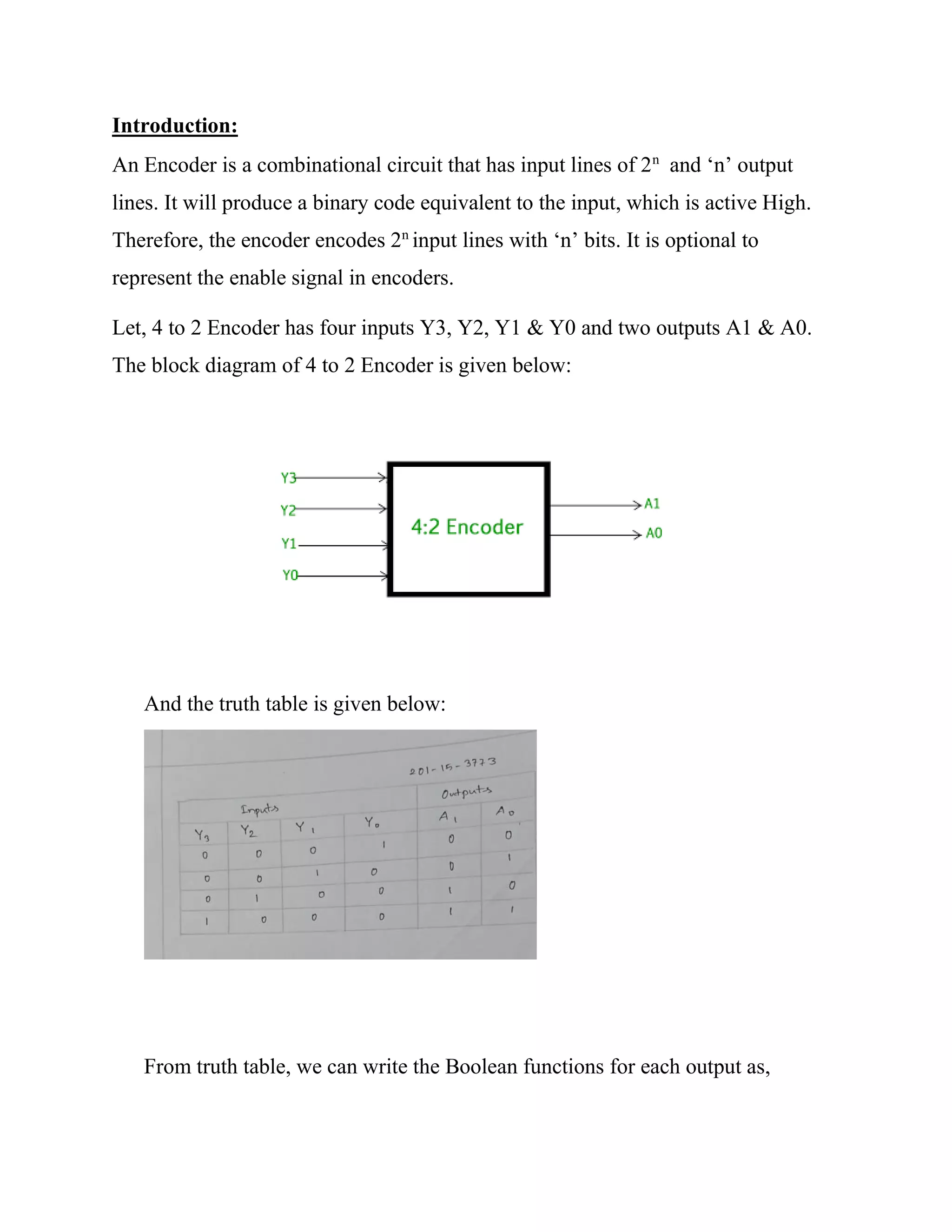
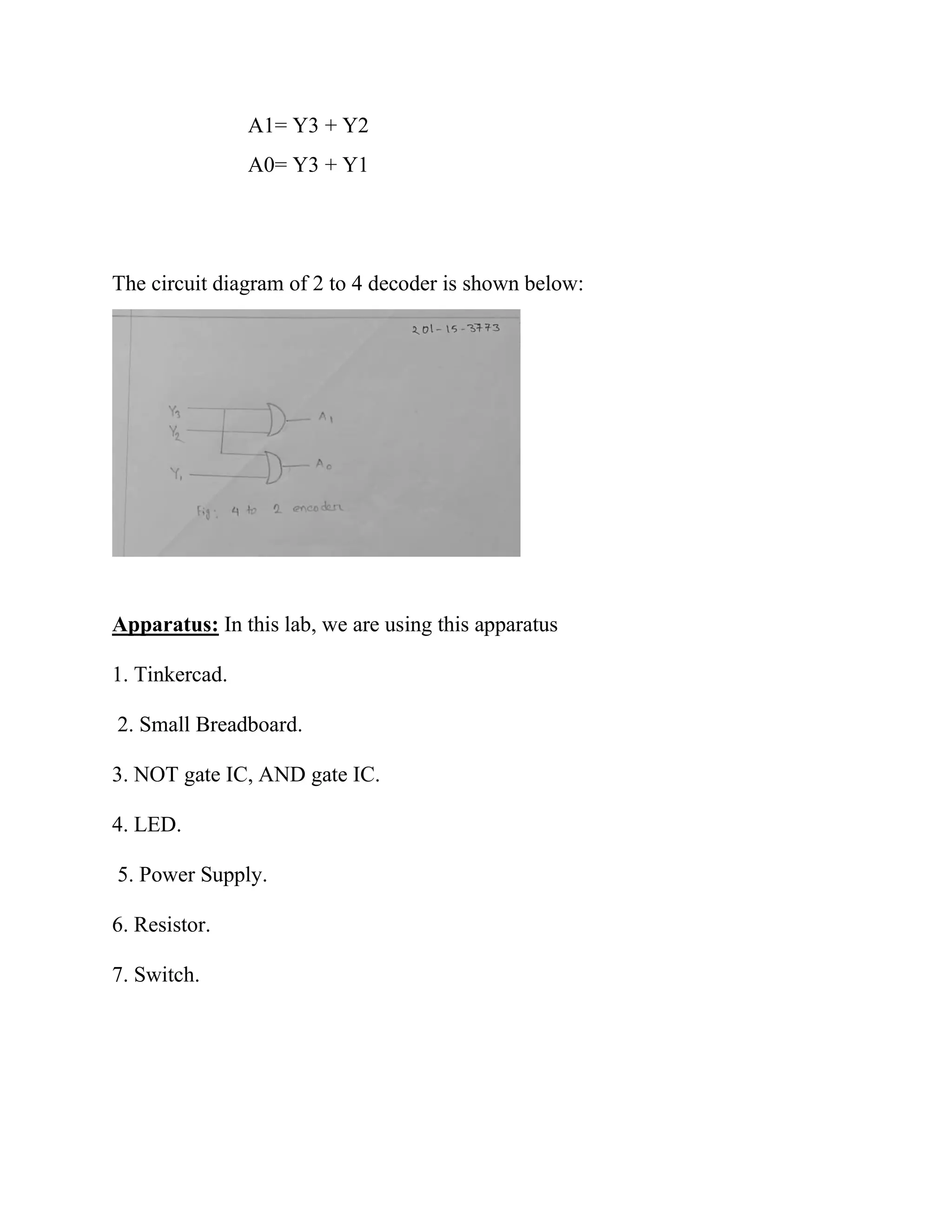
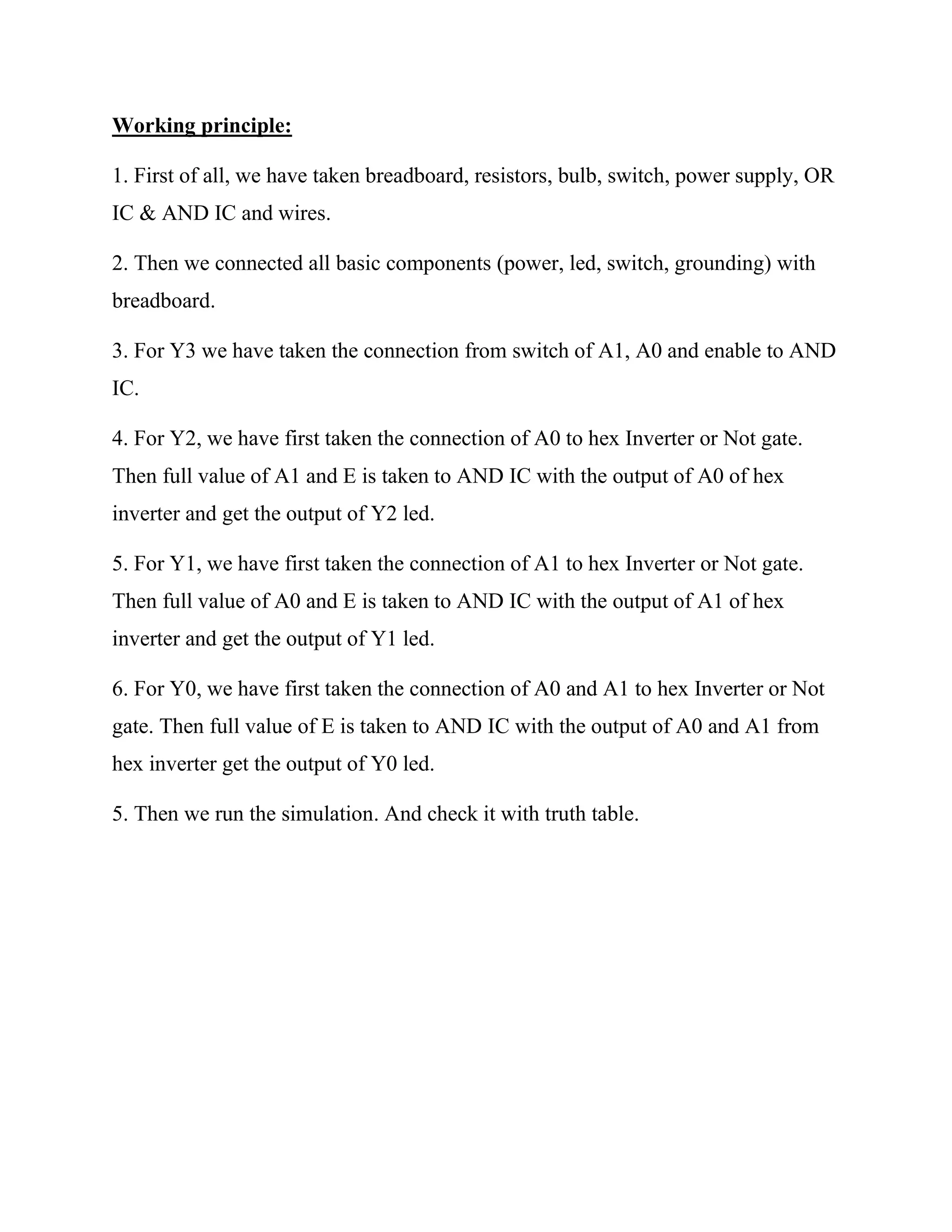
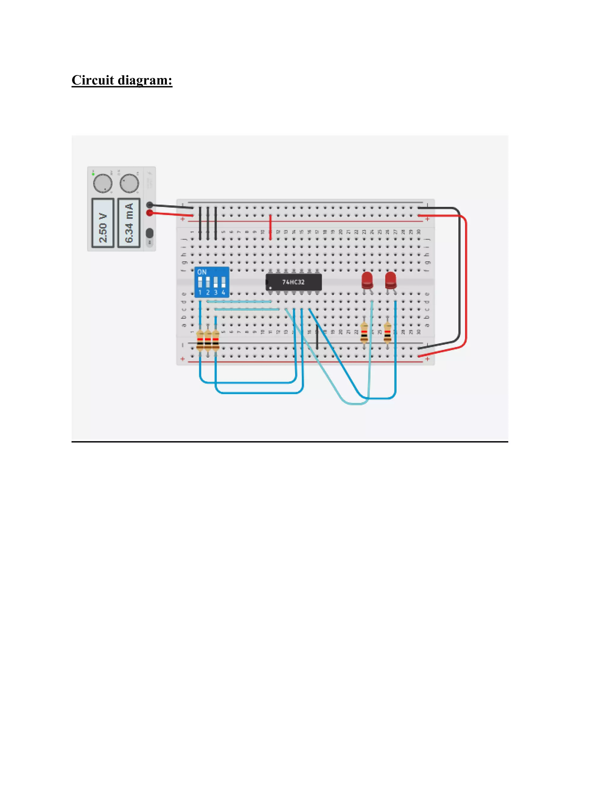
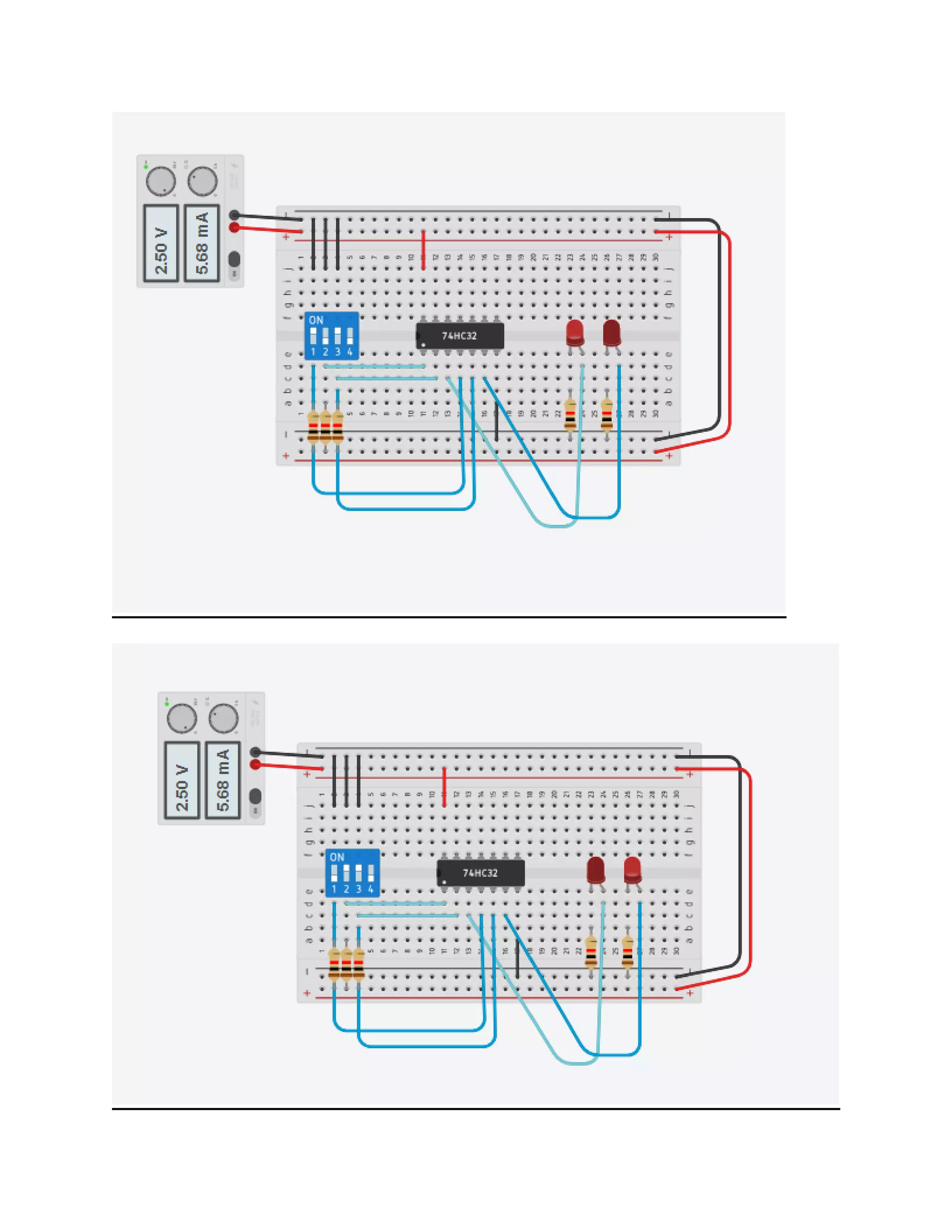
Course Title: Digital Electronics Lab
Course code: CSE224
Experiment Name: Design and Implementation of Encoder Circuits Using
Logic Gates
Submitted To:
Amir Sohel
Lecturer
Department Of CSE
Daffodil International University
Submitted By:
Name: Sajib Bormon
ID: 201 -15 - 3773
Section: PC - R
Department Of CSE
Daffodil International University
Introduction:
An Encoder is a combinational circuit that has input lines of 2n
and ‘n’ output
lines. It will produce a binary code equivalent to the input, which is active High.
Therefore, the encoder encodes 2n
input lines with ‘n’ bits. It is optional to
represent the enable signal in encoders.
Let, 4 to 2 Encoder has four inputs Y3, Y2, Y1 & Y0 and two outputs A1 & A0.
The block diagram of 4 to 2 Encoder is given below:
And the truth table is given below:
From truth table, we can write the Boolean functions for each output as,
A1= Y3 + Y2
A0= Y3 + Y1
The circuit diagram of 2 to 4 decoder is shown below:
Apparatus: In this lab, we are using this apparatus
1. Tinkercad.
2. Small Breadboard.
3. NOT gate IC, AND gate IC.
4. LED.
5. Power Supply.
6. Resistor.
7. Switch.
Working principle:
1. First of all, we have taken breadboard, resistors, bulb, switch, power supply, OR
IC & AND IC and wires.
2. Then we connected all basic components (power, led, switch, grounding) with
breadboard.
3. For Y3 we have taken the connection from switch of A1, A0 and enable to AND
IC.
4. For Y2, we have first taken the connection of A0 to hex Inverter or Not gate.
Then full value of A1 and E is taken to AND IC with the output of A0 of hex
inverter and get the output of Y2 led.
5. For Y1, we have first taken the connection of A1 to hex Inverter or Not gate.
Then full value of A0 and E is taken to AND IC with the output of A1 of hex
inverter and get the output of Y1 led.
6. For Y0, we have first taken the connection of A0 and A1 to hex Inverter or Not
gate. Then full value of E is taken to AND IC with the output of A0 and A1 from
hex inverter get the output of Y0 led.
5. Then we run the simulation. And check it with truth table.
Circuit diagram:
Description:
1. We get the output as same as we get in the truth table.
2. There is no error & risk because we run it in a simulation
software.

Sajib 201-15-3773-encoder

  • 1.
    Course Title: DigitalElectronics Lab Course code: CSE224 Experiment Name: Design and Implementation of Encoder Circuits Using Logic Gates Submitted To: Amir Sohel Lecturer Department Of CSE Daffodil International University Submitted By: Name: Sajib Bormon ID: 201 -15 - 3773 Section: PC - R Department Of CSE Daffodil International University
  • 2.
    Introduction: An Encoder isa combinational circuit that has input lines of 2n and ‘n’ output lines. It will produce a binary code equivalent to the input, which is active High. Therefore, the encoder encodes 2n input lines with ‘n’ bits. It is optional to represent the enable signal in encoders. Let, 4 to 2 Encoder has four inputs Y3, Y2, Y1 & Y0 and two outputs A1 & A0. The block diagram of 4 to 2 Encoder is given below: And the truth table is given below: From truth table, we can write the Boolean functions for each output as,
  • 3.
    A1= Y3 +Y2 A0= Y3 + Y1 The circuit diagram of 2 to 4 decoder is shown below: Apparatus: In this lab, we are using this apparatus 1. Tinkercad. 2. Small Breadboard. 3. NOT gate IC, AND gate IC. 4. LED. 5. Power Supply. 6. Resistor. 7. Switch.
  • 4.
    Working principle: 1. Firstof all, we have taken breadboard, resistors, bulb, switch, power supply, OR IC & AND IC and wires. 2. Then we connected all basic components (power, led, switch, grounding) with breadboard. 3. For Y3 we have taken the connection from switch of A1, A0 and enable to AND IC. 4. For Y2, we have first taken the connection of A0 to hex Inverter or Not gate. Then full value of A1 and E is taken to AND IC with the output of A0 of hex inverter and get the output of Y2 led. 5. For Y1, we have first taken the connection of A1 to hex Inverter or Not gate. Then full value of A0 and E is taken to AND IC with the output of A1 of hex inverter and get the output of Y1 led. 6. For Y0, we have first taken the connection of A0 and A1 to hex Inverter or Not gate. Then full value of E is taken to AND IC with the output of A0 and A1 from hex inverter get the output of Y0 led. 5. Then we run the simulation. And check it with truth table.
  • 5.
  • 7.
    Description: 1. We getthe output as same as we get in the truth table. 2. There is no error & risk because we run it in a simulation software.