Downloaded 212 times

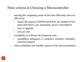
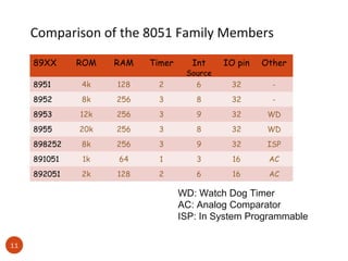
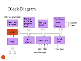
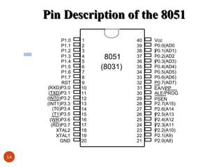
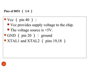
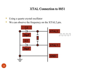
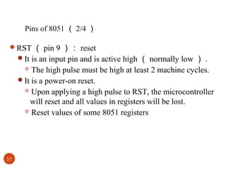


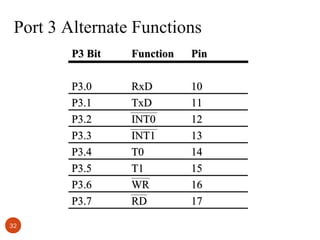
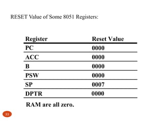
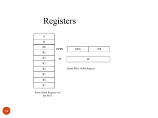
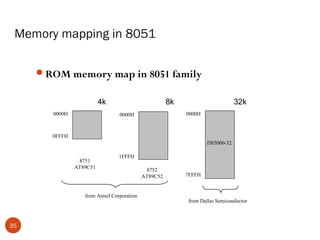
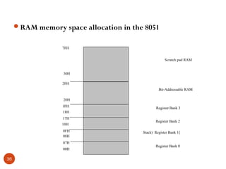
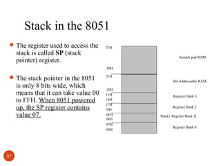
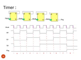
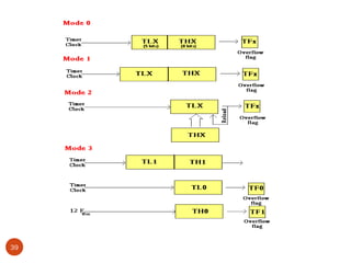

The document discusses the 8051 microcontroller. It begins with an introduction and table of contents. It then provides details about the 8051 including its block diagram, pin descriptions and functions, memory mapping, registers, stack, I/O port programming, timers, and interrupts.