Downloaded 24 times
![INNOPT -2012 7
detection function. The core facilitate interface with external
processor through the Host Processor interface and the Video
Sync Delay Circuit is used for synchronizing the input video
control signals with the output video of the core.
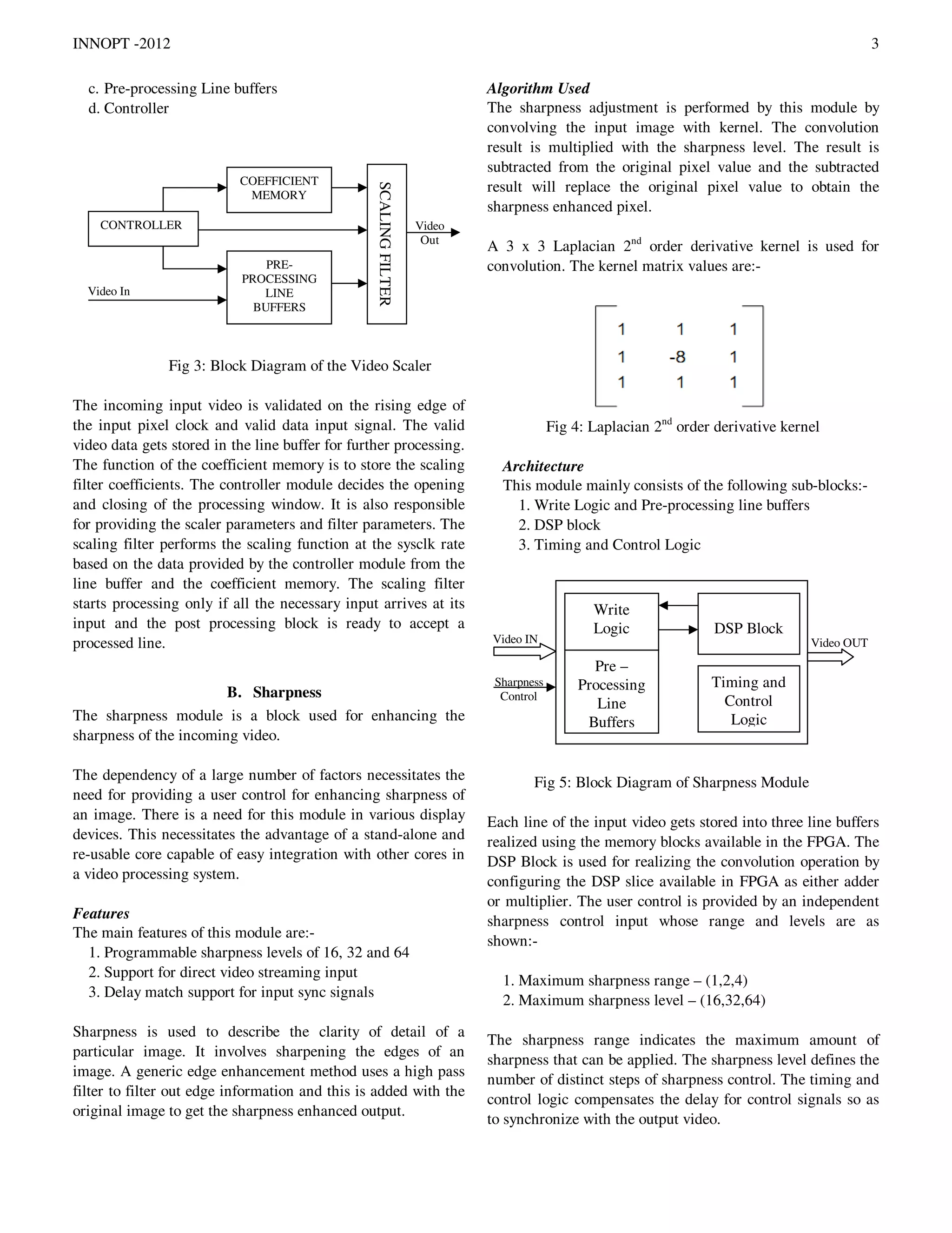
IV. RESOURCE UTILIZATION
The resource utilization of each individual core in Virtex-5
FPGA is as shown below:-
TABLE 1 Resource Utilization Summary
IP Core
Slice
Register
Slice
LUT
Block
RAM
DSP48
Clock
Frequency
Video
Scaler
7978 3900 24 21 200
Sharpness 759 673 7 27 250
Brightness 78 58 0 3 350
Contrast 31 79 0 3 350
Saturation 793 334 5 24 250
Gamma
30 24 2 0 250
Correction
VPS 16668 12625 73 82 -
* VPS or Video Processing System is an integrated system consisting of all re-usable
IP cores
The various resources available in Xilinx FPGA’s are
mainly:-
Slice Register and Slice LUT – These are blocks available
in Xilinx FPGA and are used mainly for the
implementation of logics in FPGA.
Block RAM – These are memory blocks available in Xilinx
FPGA. A total of 36Kbit of data memory is available in
Virtex-5 FPGA in the form of RAM or FIFO.
DSP48E – DSP48E is a DSP block available in Xilinx
Virtex -5 FPGA. It is capable of being configured either as
multiplier or multiplier followed by an accumulator.
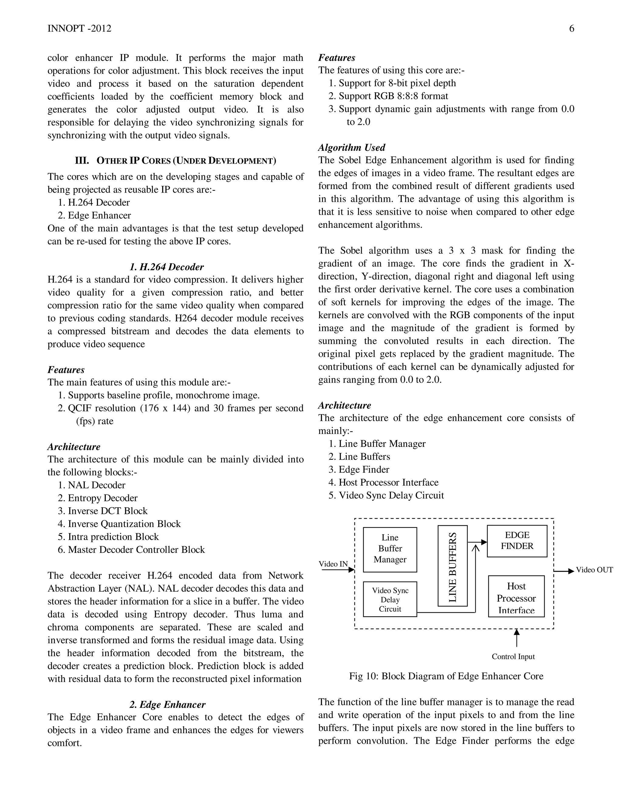
V. TEST SETUP
A test setup was developed to test all the above modules. It
was realized using the Xilinx Xtreme DSP Development Kit.
The Xilinx Xtreme DSP Development Platform (ML506) is
built around the Virtex-5 FPGA (XC5VSX50T-1FFG1136).It
contains many built-in features such as 36Kbit Block RAM
and 288 DSP slices, making it an ideal platform for testing
high performance signal applications.
The main blocks in the test setup are:-
1. Video Input Block
2. DDR2 Memory Controller
3. Scaler
4. Video Output Block
5. Picture Quality Enhancement Block
6. Gamma Correction Block
UART
Controller
Fig 11: System Architecture of Test Setup
The input video is connected to the Video ADC and the
digitized output from the Video ADC is given to FPGA as
video input. During video processing, video frames are stored
in DDR2 and is made available to FPGA for further
processing. The Video data gets processed while it passes
through the scaler block, picture quality block and the
Gamma correction block. The processed video output is
finally connected to display monitor through the Video ADC.
Control input for scaling and picture quality enhancement
block is provided from a Host PC through RS232.
VI. CONCLUSION
The goal of this project was to develop Video IP cores capable
of performing functions such as video scaling, sharpness
enhancement and picture quality enhancement. These cores,
when integrated into a single system provided a performance
equivalent to that of any ASIC based video processing
systems. This project has enabled NeST to gain sufficient
expertise in the video domain and develop more complex
video processing cores like H.264 Decoder and Edge
Enhancer.
REFERENCES
[1] NeST Video Scaler v1.0 – User Guide.
[2] NeST Sharpness Enhancer v1.0 – Datasheet
[3] NeST Gamma Correction v1.0 – User Guide
[4] NeST Contrast Enhancer v1.0 – User Guide
[5] NeST Color Enhancer v1.0 – User Guide
[6] NeST Brightness Enhancer v1.0 – User Guide
Video OUT
Video IN
DDR2
DDR2 Controller
Video Output
Block
Picture Quality
Enhancer
Video Input Block
V
I
D
E
O
A
D
C
V
I
D
E
O
D
A
C
Scaler Block
RS232
Microblaze
I2C
Controller
Sharpness
Enhancer
Block
Gamma
Correction Block](https://image.slidesharecdn.com/real-timevideoprocessinginfpga-140830034143-phpapp02/75/Real-Time-Video-Processing-in-FPGA-7-2048.jpg)

This document summarizes the development of real-time video processing IP cores in FPGA by NeST including a video scaler, sharpness enhancer, gamma correction, and picture quality enhancer modules. It describes the specifications, algorithms, and architectures of each module developed as reusable IP cores. The video scaler uses bilinear interpolation for scaling up and nearest neighbor for scaling down. The sharpness enhancer uses a Laplacian filter. Gamma correction uses programmable lookup tables. The picture quality enhancer contains brightness, contrast, and color adjustment modules. Together these cores form a video processing suite for applications like surveillance and medical imaging.