Downloaded 113 times
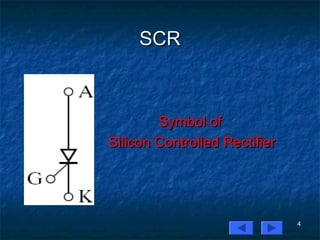
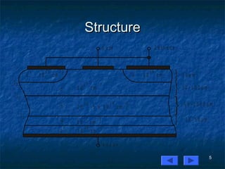
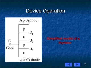
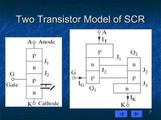
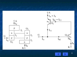
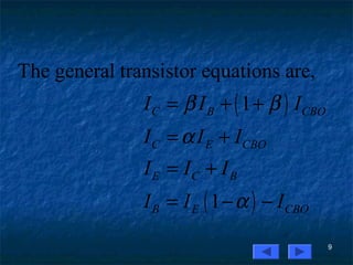
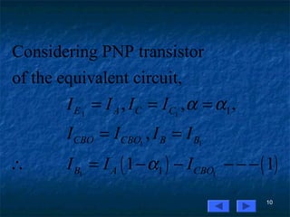
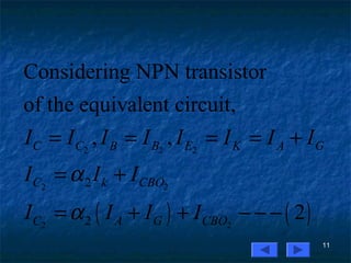
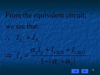
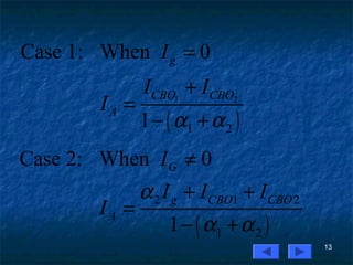
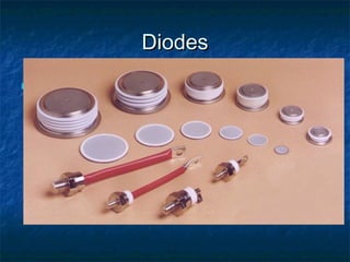
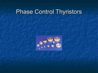
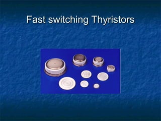
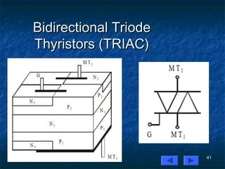
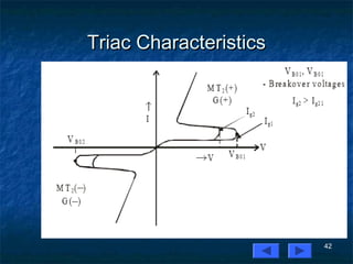


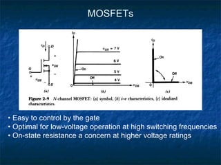
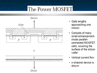
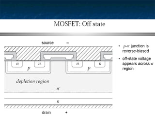
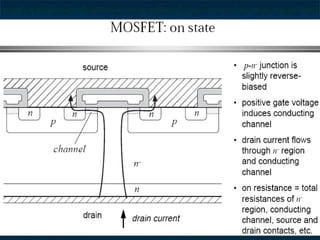

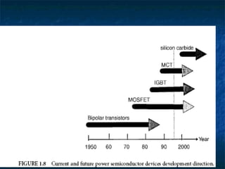

This document provides information about thyristors, which are the most important type of power semiconductor device. Thyristors have the highest power handling capability of semiconductor devices, with ratings up to 5000V/6000A and switching frequencies from 1-20kHz. Thyristors are inherently slow switching devices compared to other devices like BJTs and MOSFETs. Thyristors can be turned on by their gate but not turned off, making them useful as latching switches. The document discusses thyristor structure, operation, characteristics, types including phase control, fast switching, GTOs and TRIACs, and specifications like voltage and current ratings.


