Downloaded 365 times


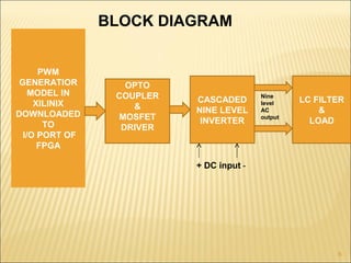
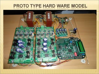

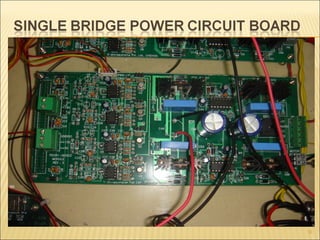


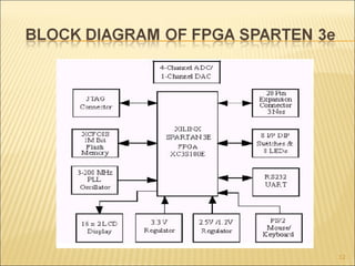


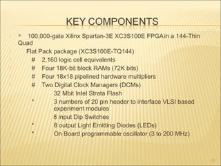


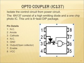
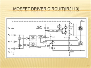
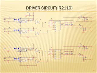
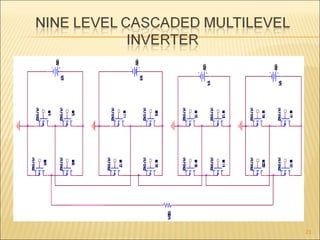


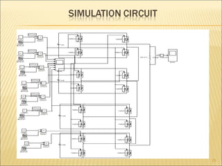
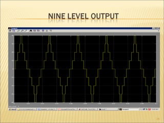
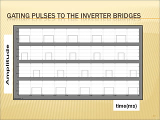
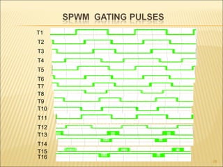
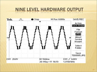
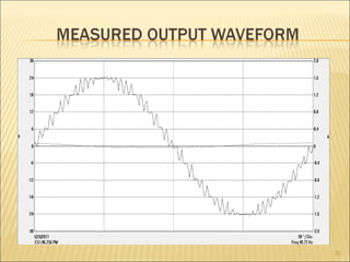

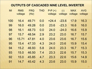

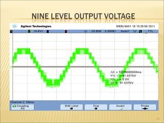
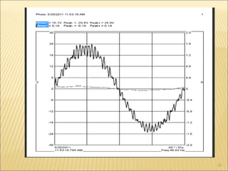
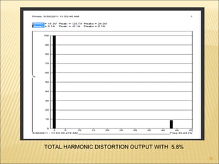


The document outlines the design and implementation of a prototype nine-level cascaded multilevel inverter using FPGA to generate desired AC output voltage via sinusoidal pulse width modulation (SPWM). It details the hardware setup, including the use of Xilinx software for signal generation and the integration of multiple full-bridge inverters for achieving varied voltage levels. Performance analysis indicates that PWM switching schemes demonstrate lower total harmonic distortion in the inverter's output.