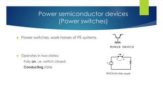
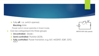
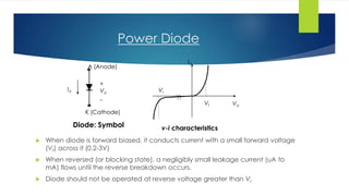
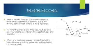
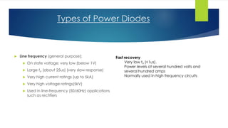
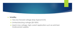
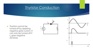
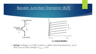
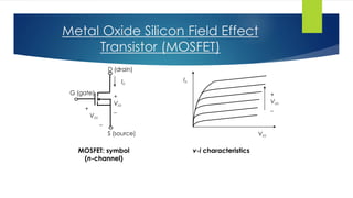
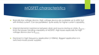
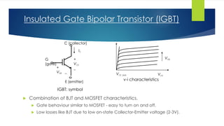
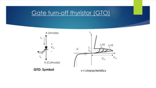
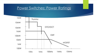
STATICS SWITCHES
PRAPERED BY:-
KATARIYA NIMESH (12EE40)
MAKWANA KRUNAL (12EE36)
SHIHORA HARSH (12EE45)
Power semiconductor devices
(Power switches)
 Power switches: work-horses of PE systems.
 Operates in two states:
Fully on. i.e. switch closed.
Conducting state
POWER SWITCH
SWITCH ON (fully closed)
Vin
Vswitch= 0
I
 Fully off , i.e. switch opened.
Blocking state
Power switch never operates in linear mode.
 Can be categorised into three groups:
 Uncontrolled: Diode :
 Semi-controlled: Thyristor (SCR).
 Fully controlled: Power transistors: e.g. BJT, MOSFET, IGBT, GTO,
IGCT
SWITCH OFF (fully opened)
Vin
Vswitch= Vin
I=0
Photos of Power Switch
• Power Diodes
Stud type
“Hockey-puck” type
• IGBT
Module type: Full
bridge and three
phase
IGCT
Integrated with
its driver
Power Diode
 When diode is forward biased, it conducts current with a small forward voltage
(Vf) across it (0.2-3V)
 When reversed (or blocking state), a negligibly small leakage current (uA to
mA) flows until the reverse breakdown occurs.
 Diode should not be operated at reverse voltage greater than Vr
A (Anode)
K (Cathode)
+
Vd
_
Id
Diode: Symbol
Id
VdVf
Vr
v-i characteristics
Reverse Recovery
 When a diode is switched quickly from forward to
reverse bias, it continues to conduct due to the
minority carriers which remains in the p-n junction.
 The minority carriers require finite time, i.e, trr (reverse
recovery time) to recombine with opposite charge and
neutralise.
 Effects of reverse recovery are increase in switching
losses, increase in voltage rating, over-voltage (spikes)
in inductive loads
IF
IRM
VR
t0
t2
trr= ( t2 - t0 )
VRM
Types of Power Diodes
 Line frequency (general purpose):
 On state voltage: very low (below 1V)
 Large trr (about 25us) (very slow response)
 Very high current ratings (up to 5kA)
 Very high voltage ratings(5kV)
 Used in line-frequency (50/60Hz) applications
such as rectifiers
Fast recovery
Very low trr (<1us).
Power levels at several hundred volts and
several hundred amps
Normally used in high frequency circuits
 Schottky
 Very low forward voltage drop (typical 0.3V)
 Limited blocking voltage (50-100V)
 Used in low voltage, high current application such as switched
mode power supplies.
Thyristor (SCR)
 If the forward breakover voltage (Vbo) is exceeded, the SCR “self-triggers”
into the conducting state
A (Anode)
K (Cathode)
+
Vak
_
Ia
Thyristor: Symbol
G (Gate)
Ig
Ia
Vak
Vr
Ig=0Ig>0
Ih
Ibo
Vbo
 The presence of gate current will reduce Vbo.
 “Normal” conditions for thyristors to turn on:
 the device is in forward blocking state (i.e Vak is positive)
 a positive gate current (Ig) is applied at the gate
 Once conducting, the anode current is latched. Vak collapses to
normal forward volt-drop, typically 1.5-3V.
 In reverse -biased mode, the SCR behaves like a diode.
Thyristor Conduction
 Thyristor cannot be
turned off by applying
negative gate current. It
can only be turned off if
Ia goes negative
(reverse)
+
vs
_
ig
ia
wt
vo
a
ig
wt
wt
vs
 This happens when negative portion of the of sine-wave occurs
(natural commutation),
 Another method of turning off is known as “forced
commutation”,The anode current is “diverted” to another
circuitry.
Types of thyristors
 Phase controlled
 rectifying line frequency voltage and current for ac and dc
motor drives
 large voltage (up to 7kV) and current (up to 4kA) capability
 low on-state voltage drop (1.5 to 3V)
 Inverter grade
 used in inverter and chopper
 Quite fast. Can be turned-on using “force-commutation”
method.
 Light activated
 Similar to phase controlled, but triggered by pulse of light.
 Normally very high power ratings
 TRIAC
 Dual polarity thyristors
Controllable switches
(power transistors)
 Can be turned “ON”and “OFF” by relatively very small control signals.
 Operated in SATURATION and CUT-OFF modes only.
 No “linear region” operation is allowed due to excessive power loss.
 In general, power transistors do not operate in latched mode.
 Traditional devices: Bipolar junction transistors (BJT), Metal oxide silicon field effect transistor (
MOSFET), Insulated gate bipolar transistors (IGBT), Gate turn-off thyristors (GTO)
 Emerging (new) devices: Gate controlled thyristors (GCT).
Bipolar Junction Transistor (BJT)
 Ratings: Voltage: VCE<1000, Current: IC<400A. Switching frequency up to
5kHz. Low on-state voltage: VCE(sat) : 2-3V
+
VCE
_
IC
IB
C (collector)
B (base)
E (emitter) VCE
IB
v-i characteristics
VCE (sat)
 Low current gain (b<10). Need high base current to obtain reasonable IC .
 Expensive and complex base drive circuit. Hence not popular in new
products.
Metal Oxide Silicon Field Effect
Transistor (MOSFET)
+
VDS
_
ID
D (drain)
G (gate)
S (source)
+
VGS
_
ID
VDS
+
VGS
_
MOSFET: symbol
(n-channel)
v-i characteristics
 Ratings: Voltage VDS<500V, current IDS<300A. Frequency f >100KHz.
For some low power devices (few hundred watts) may go up to
MHz range.
 Turning on and off is very simple.
 To turn on: VGS =+15V
 To turn off: VGS =0 V and 0V to turn off.
 Gate drive circuit is simple
MOSFET characteristics
 Basically low voltage device. High voltage device are available up to 600V but
with limited current. Can be paralleled quite easily for higher current capability.
 Internal (dynamic) resistance between drain and source during on state, RDS(ON), ,
limits the power handling capability of MOSFET. High losses especially for high
voltage device due to RDS(ON) .
 Dominant in high frequency application (>100kHz). Biggest application is in
switched-mode power supplies.
Insulated Gate Bipolar Transistor (IGBT)
 Combination of BJT and MOSFET characteristics.
 Gate behaviour similar to MOSFET - easy to turn on and off.
 Low losses like BJT due to low on-state Collector-Emitter voltage (2-3V).
IGBT: symbol
+
VCE
_
IC
C (collector)
G
(gate)
E (emitter)
+
VGE _
VCE
VGE
v-i characteristics
VCE (sat)
Gate turn-off thyristor (GTO)
v-i characteristics
A (Anode)
K (Cathode)
+
Vak
_
Ia
GTO: Symbol
Ig
Ia
Vak
Vr
Ig=0Ig>0
Ih
Ibo
Vbo
 Behave like normal thyristor, but can be turned off using gate signal
 However turning off is difficult. Need very large reverse gate current
(normally 1/5 of anode current).
 Gate drive design is very difficult due to very large reverse gate current at
turn off.
 Ratings: Highest power ratings switch: Voltage: Vak<5kV; Current: Ia<5kA.
Frequency<5KHz.
 Very stiff competition:
Low end-from IGBT. High end from IGCT
Power Switches: Power Ratings
10Hz 1kHz 1MHz100kHz 10MHz
1kW
100kW
10kW
10MW
1MW
10MW
1GW
100W
MOSFET
IGBT
GTO/IGCT
Thyristor
Statics switches

Statics switches

  • 1.
    STATICS SWITCHES PRAPERED BY:- KATARIYANIMESH (12EE40) MAKWANA KRUNAL (12EE36) SHIHORA HARSH (12EE45)
  • 2.
    Power semiconductor devices (Powerswitches)  Power switches: work-horses of PE systems.  Operates in two states: Fully on. i.e. switch closed. Conducting state POWER SWITCH SWITCH ON (fully closed) Vin Vswitch= 0 I
  • 3.
     Fully off, i.e. switch opened. Blocking state Power switch never operates in linear mode.  Can be categorised into three groups:  Uncontrolled: Diode :  Semi-controlled: Thyristor (SCR).  Fully controlled: Power transistors: e.g. BJT, MOSFET, IGBT, GTO, IGCT SWITCH OFF (fully opened) Vin Vswitch= Vin I=0
  • 4.
    Photos of PowerSwitch • Power Diodes Stud type “Hockey-puck” type • IGBT Module type: Full bridge and three phase IGCT Integrated with its driver
  • 5.
    Power Diode  Whendiode is forward biased, it conducts current with a small forward voltage (Vf) across it (0.2-3V)  When reversed (or blocking state), a negligibly small leakage current (uA to mA) flows until the reverse breakdown occurs.  Diode should not be operated at reverse voltage greater than Vr A (Anode) K (Cathode) + Vd _ Id Diode: Symbol Id VdVf Vr v-i characteristics
  • 6.
    Reverse Recovery  Whena diode is switched quickly from forward to reverse bias, it continues to conduct due to the minority carriers which remains in the p-n junction.  The minority carriers require finite time, i.e, trr (reverse recovery time) to recombine with opposite charge and neutralise.  Effects of reverse recovery are increase in switching losses, increase in voltage rating, over-voltage (spikes) in inductive loads IF IRM VR t0 t2 trr= ( t2 - t0 ) VRM
  • 7.
    Types of PowerDiodes  Line frequency (general purpose):  On state voltage: very low (below 1V)  Large trr (about 25us) (very slow response)  Very high current ratings (up to 5kA)  Very high voltage ratings(5kV)  Used in line-frequency (50/60Hz) applications such as rectifiers Fast recovery Very low trr (<1us). Power levels at several hundred volts and several hundred amps Normally used in high frequency circuits
  • 8.
     Schottky  Verylow forward voltage drop (typical 0.3V)  Limited blocking voltage (50-100V)  Used in low voltage, high current application such as switched mode power supplies.
  • 9.
    Thyristor (SCR)  Ifthe forward breakover voltage (Vbo) is exceeded, the SCR “self-triggers” into the conducting state A (Anode) K (Cathode) + Vak _ Ia Thyristor: Symbol G (Gate) Ig Ia Vak Vr Ig=0Ig>0 Ih Ibo Vbo
  • 10.
     The presenceof gate current will reduce Vbo.  “Normal” conditions for thyristors to turn on:  the device is in forward blocking state (i.e Vak is positive)  a positive gate current (Ig) is applied at the gate  Once conducting, the anode current is latched. Vak collapses to normal forward volt-drop, typically 1.5-3V.  In reverse -biased mode, the SCR behaves like a diode.
  • 11.
    Thyristor Conduction  Thyristorcannot be turned off by applying negative gate current. It can only be turned off if Ia goes negative (reverse) + vs _ ig ia wt vo a ig wt wt vs
  • 12.
     This happenswhen negative portion of the of sine-wave occurs (natural commutation),  Another method of turning off is known as “forced commutation”,The anode current is “diverted” to another circuitry.
  • 13.
    Types of thyristors Phase controlled  rectifying line frequency voltage and current for ac and dc motor drives  large voltage (up to 7kV) and current (up to 4kA) capability  low on-state voltage drop (1.5 to 3V)  Inverter grade  used in inverter and chopper  Quite fast. Can be turned-on using “force-commutation” method.
  • 14.
     Light activated Similar to phase controlled, but triggered by pulse of light.  Normally very high power ratings  TRIAC  Dual polarity thyristors
  • 15.
    Controllable switches (power transistors) Can be turned “ON”and “OFF” by relatively very small control signals.  Operated in SATURATION and CUT-OFF modes only.  No “linear region” operation is allowed due to excessive power loss.  In general, power transistors do not operate in latched mode.  Traditional devices: Bipolar junction transistors (BJT), Metal oxide silicon field effect transistor ( MOSFET), Insulated gate bipolar transistors (IGBT), Gate turn-off thyristors (GTO)  Emerging (new) devices: Gate controlled thyristors (GCT).
  • 16.
    Bipolar Junction Transistor(BJT)  Ratings: Voltage: VCE<1000, Current: IC<400A. Switching frequency up to 5kHz. Low on-state voltage: VCE(sat) : 2-3V + VCE _ IC IB C (collector) B (base) E (emitter) VCE IB v-i characteristics VCE (sat)
  • 17.
     Low currentgain (b<10). Need high base current to obtain reasonable IC .  Expensive and complex base drive circuit. Hence not popular in new products.
  • 18.
    Metal Oxide SiliconField Effect Transistor (MOSFET) + VDS _ ID D (drain) G (gate) S (source) + VGS _ ID VDS + VGS _ MOSFET: symbol (n-channel) v-i characteristics
  • 19.
     Ratings: VoltageVDS<500V, current IDS<300A. Frequency f >100KHz. For some low power devices (few hundred watts) may go up to MHz range.  Turning on and off is very simple.  To turn on: VGS =+15V  To turn off: VGS =0 V and 0V to turn off.  Gate drive circuit is simple
  • 20.
    MOSFET characteristics  Basicallylow voltage device. High voltage device are available up to 600V but with limited current. Can be paralleled quite easily for higher current capability.  Internal (dynamic) resistance between drain and source during on state, RDS(ON), , limits the power handling capability of MOSFET. High losses especially for high voltage device due to RDS(ON) .  Dominant in high frequency application (>100kHz). Biggest application is in switched-mode power supplies.
  • 21.
    Insulated Gate BipolarTransistor (IGBT)  Combination of BJT and MOSFET characteristics.  Gate behaviour similar to MOSFET - easy to turn on and off.  Low losses like BJT due to low on-state Collector-Emitter voltage (2-3V). IGBT: symbol + VCE _ IC C (collector) G (gate) E (emitter) + VGE _ VCE VGE v-i characteristics VCE (sat)
  • 22.
    Gate turn-off thyristor(GTO) v-i characteristics A (Anode) K (Cathode) + Vak _ Ia GTO: Symbol Ig Ia Vak Vr Ig=0Ig>0 Ih Ibo Vbo
  • 23.
     Behave likenormal thyristor, but can be turned off using gate signal  However turning off is difficult. Need very large reverse gate current (normally 1/5 of anode current).  Gate drive design is very difficult due to very large reverse gate current at turn off.  Ratings: Highest power ratings switch: Voltage: Vak<5kV; Current: Ia<5kA. Frequency<5KHz.  Very stiff competition: Low end-from IGBT. High end from IGCT
  • 24.
    Power Switches: PowerRatings 10Hz 1kHz 1MHz100kHz 10MHz 1kW 100kW 10kW 10MW 1MW 10MW 1GW 100W MOSFET IGBT GTO/IGCT Thyristor