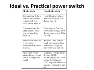
This document provides an overview of power semiconductor devices and their characteristics. It discusses various power devices including diodes, thyristors, transistors, and their construction and operating principles. Key points covered include:
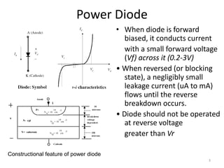
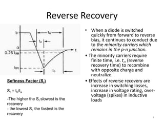
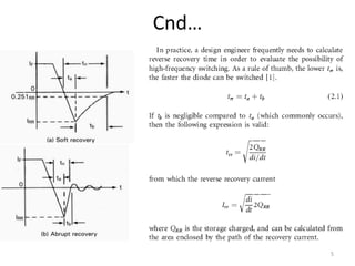
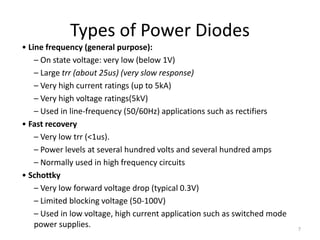
- Power diodes can conduct current in the forward bias state and block it in reverse bias, but require a recovery time when switched from on to off.
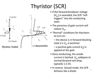
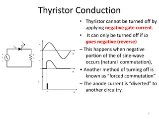
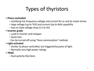
- Thyristors like SCRs can latch on in the forward conducting state and require the current to go to zero to turn off, while TRIACs are dual polarity thyristors.
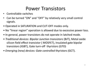
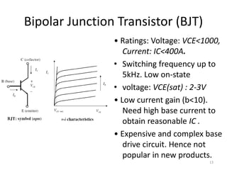
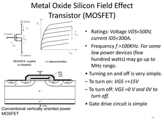
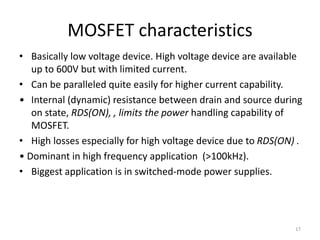
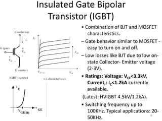
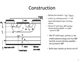
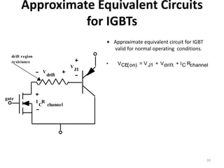
- Power transistors like IGBTs, MOSFETs, and BJTs can be precisely controlled on and off but require heat sinking due