Download as PDF, PPTX

![Features of 8255
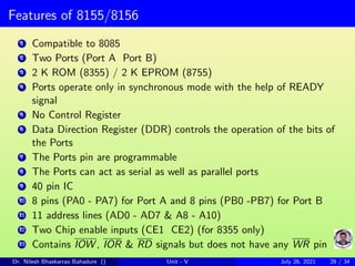
1. Compatible to 8085
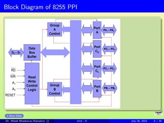
2. Three Ports (Port A, Port B & Port C) [All ports are of 8 bits]
3. Port A & Port B act as parallel ports whereas Port C can act as parallel
as well as serial port
4. Port C supply the Handshake signals for Port A and Port B
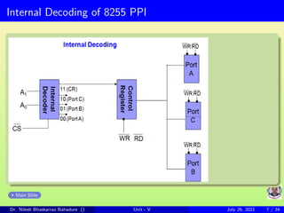
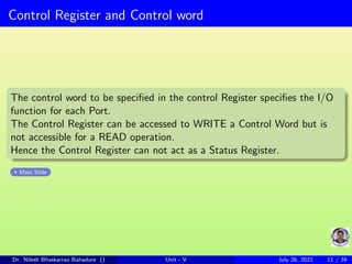
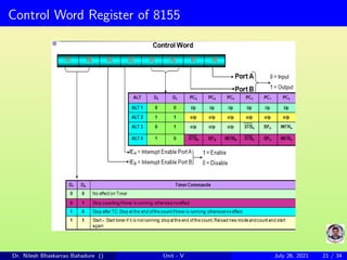
5. Only Command Register but no Status Register, i.e., the Command
Register can not act as Status Register
6. 40 pin IC
7. 8 pins (PA0 - PA7) for Port A, 8 pins (PB0 - PB7) for Port B and 8
pins (PC0 - PC7) for Port C
8. No memory or other application registers
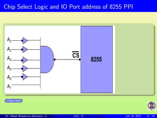
9. One Chip Select input (CS)
10. Contains RD and WR signals but no IO/M is required.
Main Slide
Dr. Nilesh Bhaskarrao Bahadure () Unit - V July 26, 2021 5 / 34](https://image.slidesharecdn.com/peripheralsofmicroprocessor8085ho-210726080519/85/Peripherals-of-Microprocessor-8085-5-320.jpg)
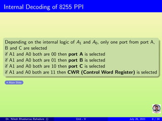
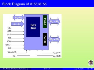
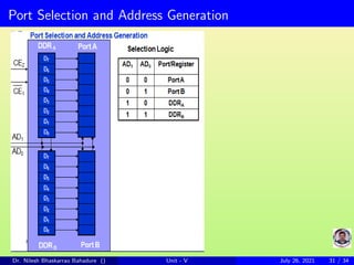
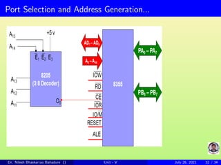
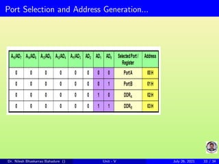


The document provides an overview of the architecture and features of various peripheral interfacing devices, specifically the 8255, 8155/8156, and 8355/8755 integrated circuits. It details their functionalities such as programmable input/output ports, control registers, timer modes, and application in interfacing with 8085 microprocessors. Additionally, the document includes block diagrams and operational modes of the mentioned devices.