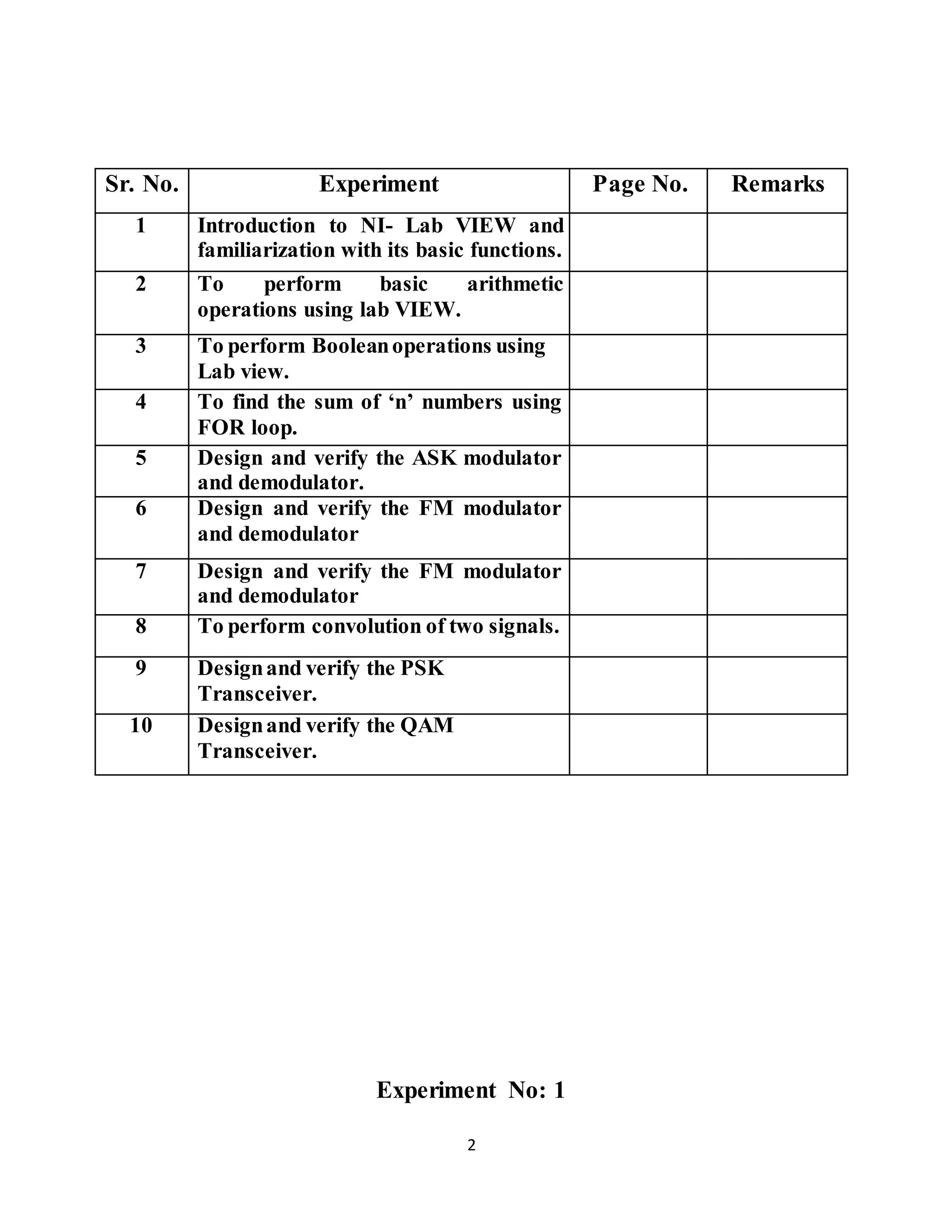
The document describes 10 experiments conducted using LabVIEW:
1) Introduction to LabVIEW and its basic functions.
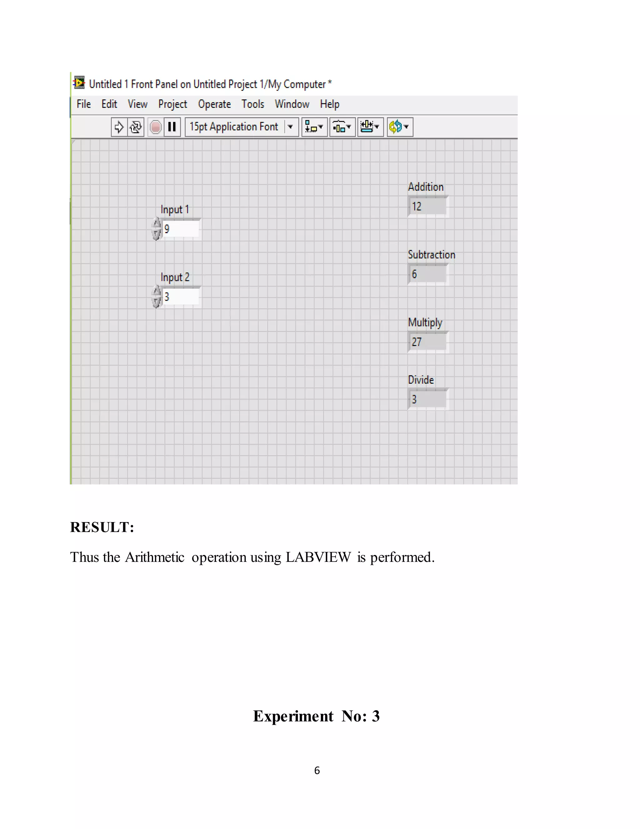
2) Performing basic arithmetic operations using LabVIEW.
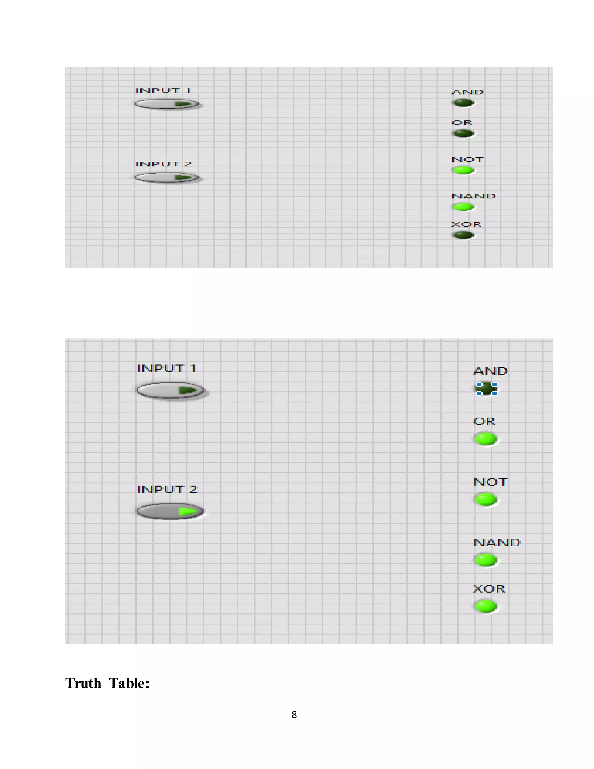
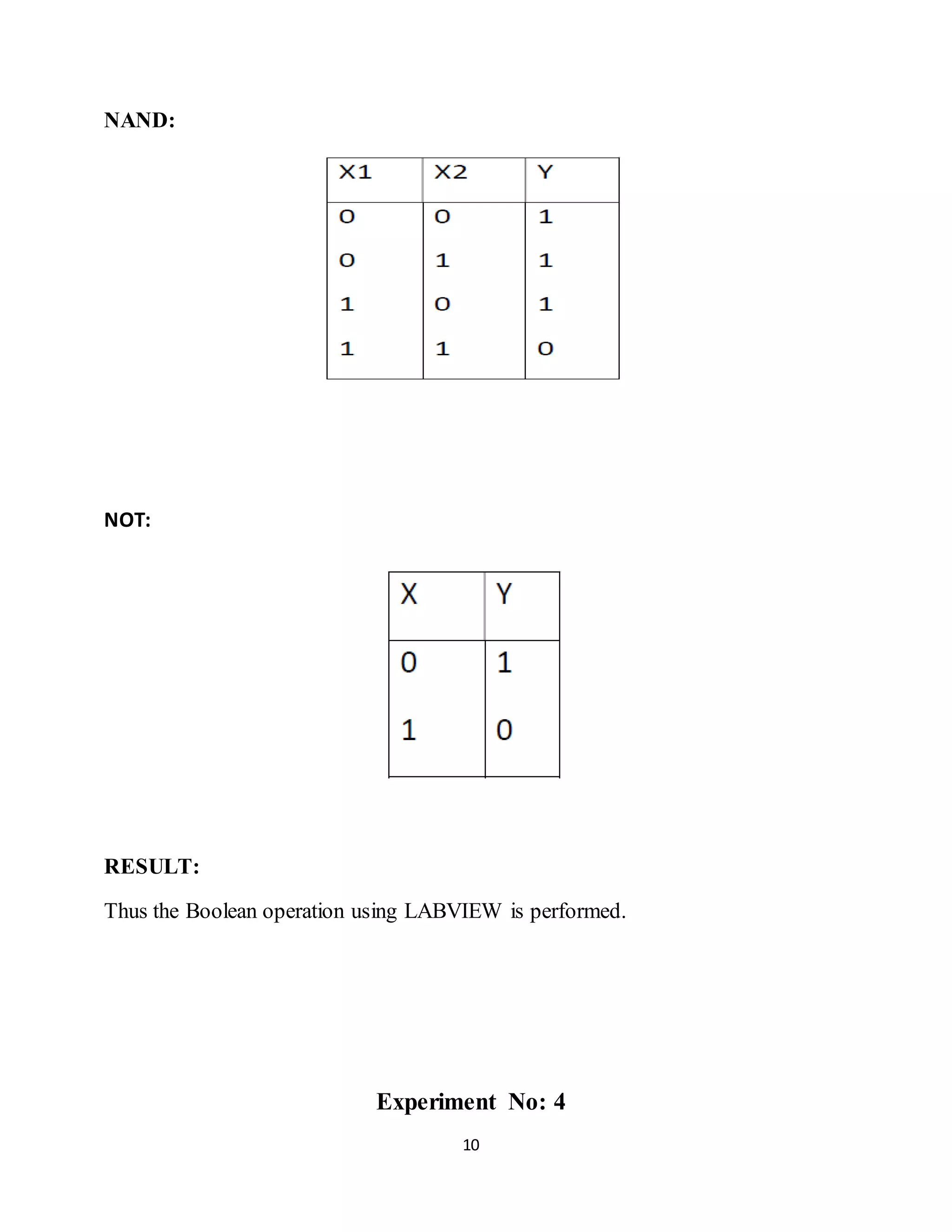
3) Performing Boolean operations using LabVIEW.
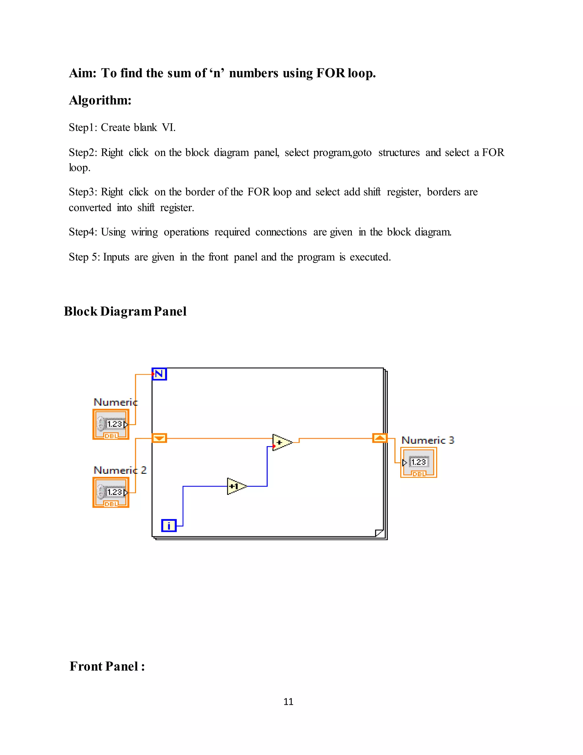
4) Finding the sum of 'n' numbers using a FOR loop.
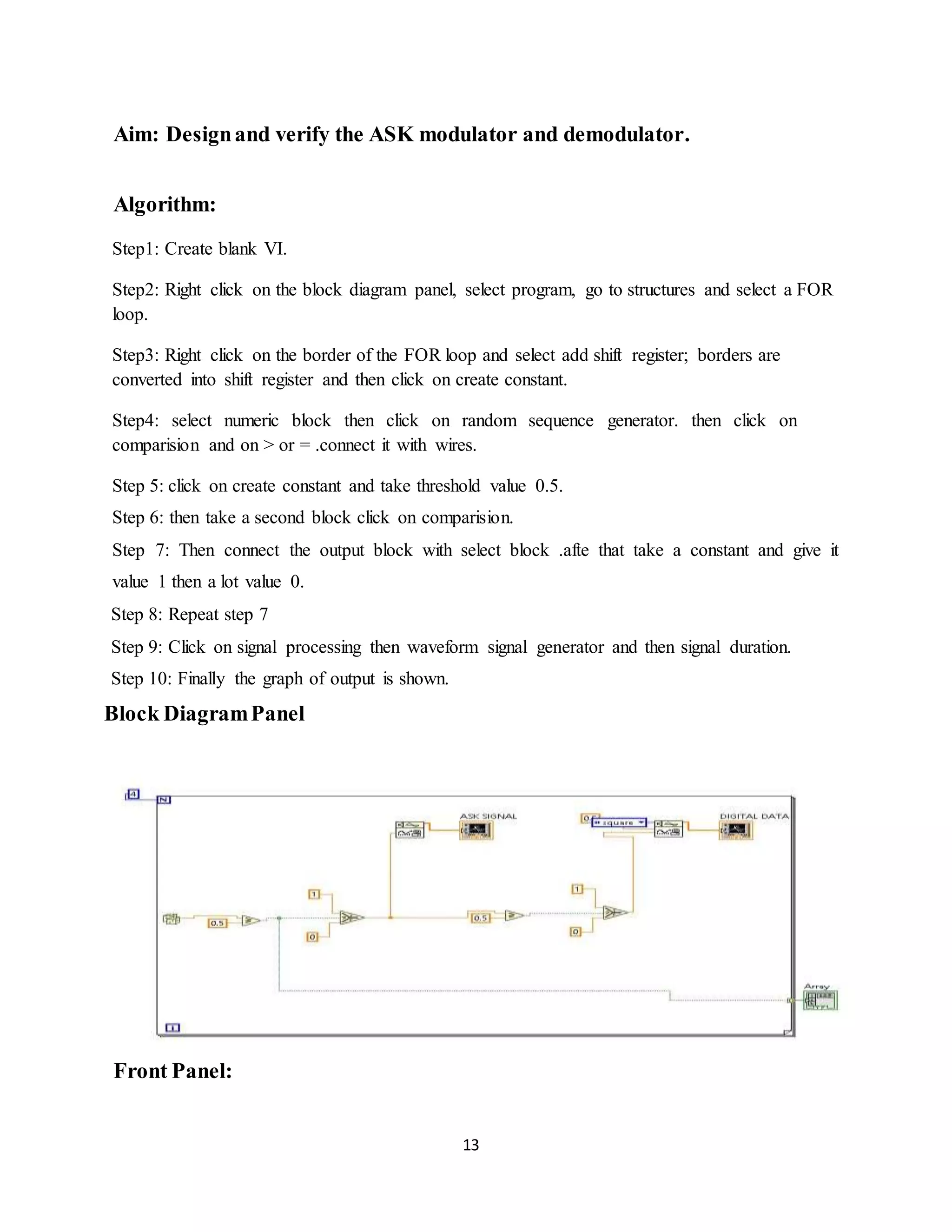
5) Designing and verifying an ASK modulator and demodulator.
6) Designing and verifying an FSK modulator and demodulator.
7) Designing and verifying an FM modulator and demodulator.
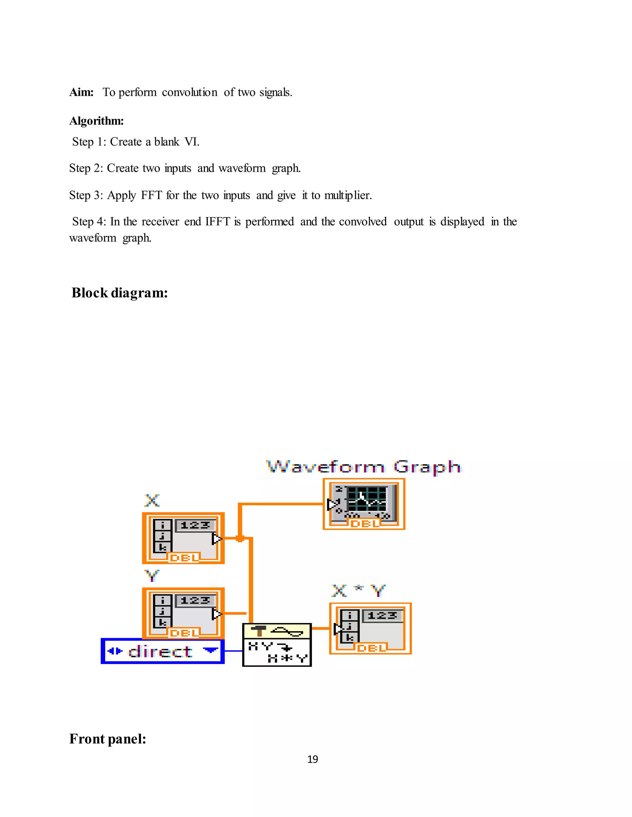
8) Performing convolution of two signals.
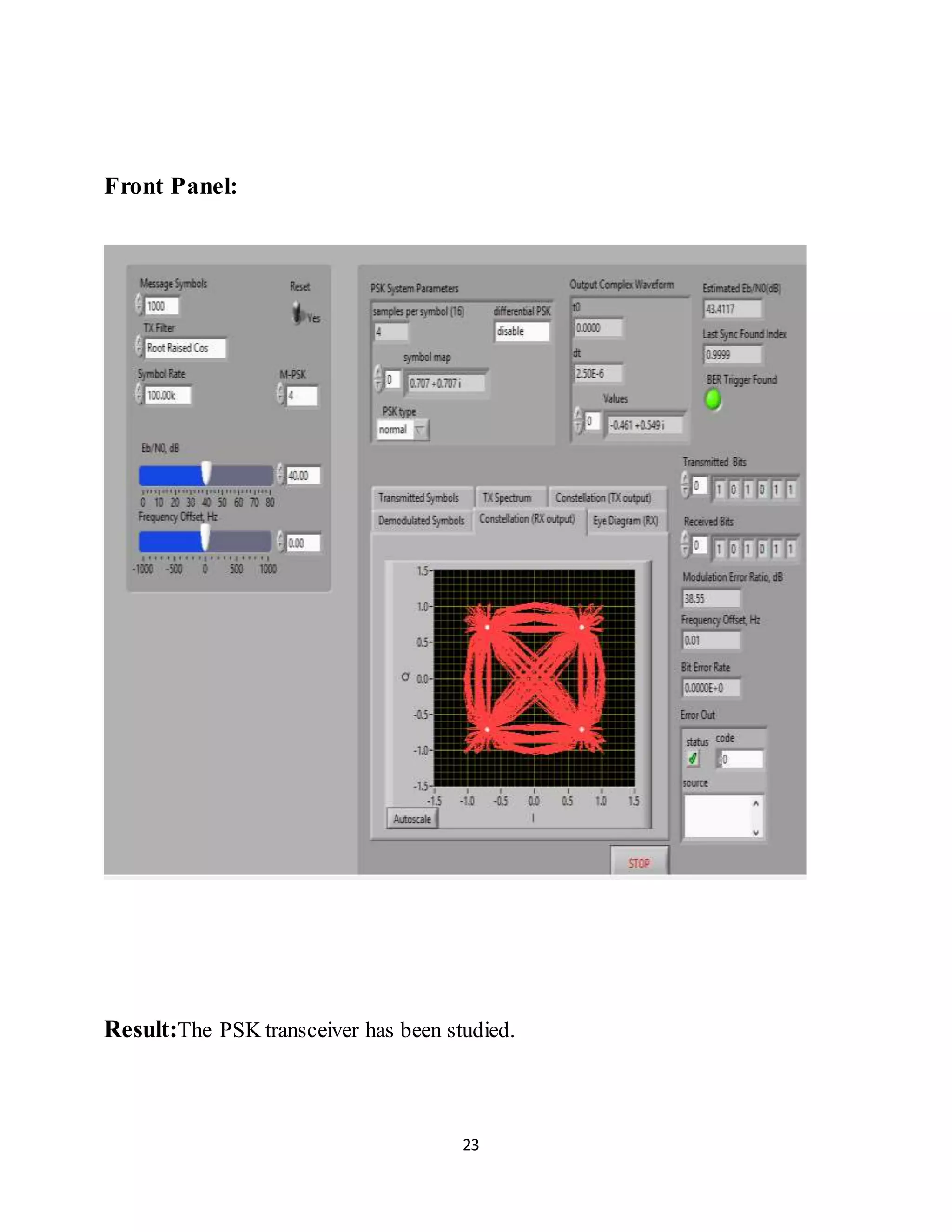
9) Designing and verifying a PSK transceiver.
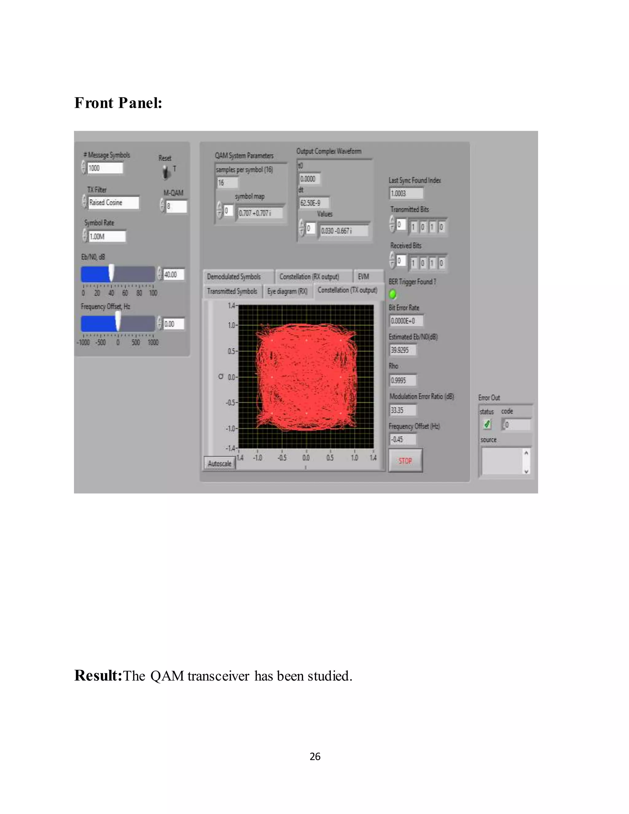
10) Designing