The document presents a generic architecture for an area-efficient 4-input binary coded decimal (BCD) adder implemented on an FPGA. It modifies a previously proposed area-efficient 3-input decimal adder to support a generic number of inputs. The proposed 4-input adder has four stages: 1) carry save addition and propagation/generation signal generation, 2) carry network, 3) correction stage, and 4) final addition. Simulation results on a Xilinx FPGA for different number of bits and inputs are presented, showing the adder has reduced delay and area compared to previous approaches. The generic approach can support addition of any number of inputs.

![Figure. . 1 Conventional hardware architecture for
performing the addition of three inputs of four digits
digits.
If the input bits are increased the number of full adder
are also increased so the propagation delay is
So reduced delay BCD adder is proposed for fast
calculation.
increased.
Figure.2 The hardware for performing the addition of
three inputs of four digits.
.2 From figure.2 addition of 3-input of 4
4-digit reduced
delay BCD adder, propagation delay is reduced, but on
chip consumed area is increased due to carry network
and an analyzer.
So the modification made regarding this
approach is area-efficient 3-input
of 4-digit each,
decimal adder presented in [13].There are
three stages
in this adder first stage is adder + analyzer it takes three
inputs of 4-digits and generate sum using carry look
look-here
ahead adder(CLA). There are two signal which is
DP(Digit Propagate)and DG(Digit Generate). When the
sum of three valid id BCD numbers is greater then 9 and
19 these conditions are identified by DG
DGi. When the sum
of three BCD numbers is 9,8,18 or 19, these condition
are identified by DPi, where, i==0 to 3.
Figure.3- The Architecture of 3
3-input Adder+Analyzer
for producing DG & DP
In second stage,
DGi and DPi signals are
sent to carry network which is composed by parallel
prefix adder to generate the decimal carry.
Cout[i] = DGi + DPi . Cin[i
i-1]
And stage 3 is correction stage which added in parallel
to the binary sums produced by the stage 1 to produce
the real decimal sums Results[15:0].
In this 3-input
reduced delay BCD adder, r, propagation delay is reduced
as well as chip consumed area is
also reduced .
Figure.4 the one-digit hardware proposed for 3
CSA+ PG Generator circuit
But this proposed model
3-inputs
is limited for fixed
number of input digits. i.e. Limited number of digits in
input.
Thus, in the next Section our proposed model
modified the previous model with reduced delay and
high area efficiency through generic
input.
approach of 4-
75](https://image.slidesharecdn.com/paperid-27201434-140904033816-phpapp01/85/Paper-id-27201434-2-320.jpg)
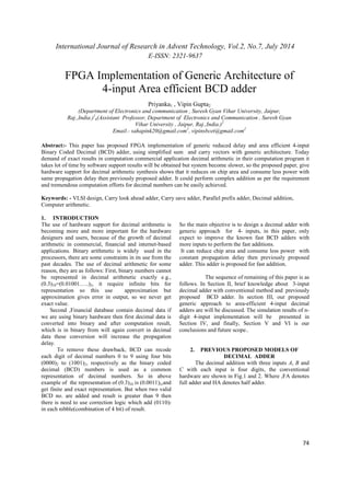
![3. PROPOSED GENERIC ARCHITECTURE OF
AREA- EFFICIENT DECIMAL ADDER WITH
FOUR INPUTS
The proposed model is consisting of FPGA
implementation of generic reduced delay and area
efficient 4-input BCD adder. It is the modification
Area Efficient 3-input Decimal adders using simplified
carry and sum vectors , presented in
generator rator circuits and the recursive generation gen
of
correction terms, this proposed decimal adders could
perform efficient summations with 'm' inputs with 'n'
number of digits of operands. The proposed BCD adder
consists of four stages, each input is divided into n
In proposed design has
of
[].Using proposed
n- bits.
perform decimal
each input is n-bits
addition with 4 inputs A,B,C,D with
and sent to the CSA+PG Generator to product the digit
sums and carries arries with digit propagation
and generation
signals, then using Carry Network to
obtain the real
decimal carries, in the last stage the sums can be
computed by adding the digit sums and
carries with
correction values using carry save adders (CSA) plus
bit carry look-ahead adders (CLA).
signals for each digit are computed by Carry Network in
a parallel-prefix way, the carry propagation for the last
stage can be removed.
n-
Since the correction
Figure.5. The one-digit hardware of our proposed CSA+
PG Generator nerator circuit.
As there are four inputs, use of carry save adders
adders(CSA)
to produce sums S[(4*i)+3:4*i] and the carries
C[(4*i)+3:4*i] of four inputs first. T
signals to indicate the conditions of sums and the
corresponding logical expressions, in the design of PG
Generator, are shown in Table I. The digit generation
signal is composed of 2-bit signals, which identifies if
the sums are greater than 9,19 or
propagation signal is composed of 3
identifies the sums are equal to 7, 8, 9,17, 18,19,27,28
and 29 since the decimal carry-ins may be 0, 1,2 and 3
depending upon the carry-outs from the lower digits.
The use of following
,19 29. The digit
3-bit signals, which
Table I: The digit generation and propagation signals for
identifying the conditions of sums in each digit
Signals Conditions of the sum in each digit
DGi[1] >9
DGi[2] >19
DGi[3] >29
DPi[1] =9
DPi[2] =8
DPi[3] =7
DPi[4] =19
DPi[5] =18
DPi[6] =17
DPi[7] =29
DPi[8] =28
DPi[9] =27
The addition of 4-inputs
can reduced the delay and it is more area efficient.
Figure.6 The architecture of our proposed N
input decimal Adder
4. SUMULATION RESULTS
The code which has been proposed
efficient decimal adders with four inputs using VHDL
programming and synthesized using
having modelsim 5.4a with project navigator
Let’s take numerical example
result's snapshots for diffirent n
Example1.
When, No. of bits(n)=16,
of n-bits architecture
N- digit four
are generic area-efficient
Xilinx software
navigator.
examples and their simulation
t's n-bits for each 4-inputs
76](https://image.slidesharecdn.com/paperid-27201434-140904033816-phpapp01/85/Paper-id-27201434-3-320.jpg)
![No. of digits (m) = 4
A=7865
B=3482
C=9634
D=3482
Figure.7.1 Simulation results of Examples-1
Example2.
When, n=24 and m=6
A=347621
B=567438
C=236547
D=686461
Figure.7.2- Simulation results of Examples-2
5. CONCLUSION
The Proposed FPGA implementation of generic
area efficient four input i.e., each having m- digits and
n-bits, adder using CSA and CLA is coded in VHDL.
This adder presents minimum delay compare to
previous adder and it acquire less chip area and power
consumption is also lesser than other adder by using
power prime.
This generic approach for 4-inputs in future can
be perform addition for multiple input. In future, this
generic approach for 4-input, is further can be perform
addition for multiple inputs with reduced delay and high
area efficiency.
REFERENCES
[1]. M. S. Schmookler and A.W.Weinberger. ‘‘High
Speed Decimal Addition,’’ IEEE Transactions
on Computers, Vol. 20, No. 8, pp.862--867, Aug.
1971.
[2].M. A. Erle, M. J. Schulte, and J. M. Linebarger,
“Potential speedup using decimal floating-point
hardware,” Proc. of the Thirty-Sixth Asilomar
Conference on Signals, Systems and Computers,
Vol. 2, pp.1073–1077, Nov. 2002.
[3]. M. F. Cowlishaw, “Decimal Floating-Point:
Algorism for Computers,” Proc. of 16th IEEE
Symposium on Computer Arithmetic (ARITH-16),
pp. 104–111, June 2003.
[4]. R.D. Kenney and M.J. Schulte, ‘‘Multioperand
Decimal Addition,’’Proc. IEEE Computer Society
Ann. Symp. VLSI, pp. 251-253, Feb.2004.
[5]. R.D. Kenney and M.J. Schulte, ‘‘High-speed
multioperand decimaladders,’’ IEEE Transactions
on Computers, pp. 953-963, Vol. 54, No.8, Aug.
2005.
[6] A. Bayrakci and A. Akkas, “Reduced delay BCD
adder,” Proc. IEEE 18th International Conference
on Application-specific Systems, Architectures and
Processors, (ASAP), pp. 266-271, July 2007.
[7]. G. Bioul, M. Vazquez, J. P. Deschamps, and G.
Sutter, "Decimal addition in FPGA," Proc. SPL. 5th
Southern Conference on Programmable Logic, pp.
101-108, 2009.
[8]. H. Nikmehr, B. Phillips, and C. -C. Lim "Fast
Decimal Floating-Point Division," IEEE
Transactions on Very Large Scale Integration
(VLSI) Systems, Vol. 14, No. 9, pp. 951-961, Sept.
2006.
[9]. T. Lang, and A. Nannarelli, "Division Unit for
Binary Integer Decimals," Prof. 20th IEEE
International Conference on Application-specific
Systems, Architectures and Processors (ASAP),pp.
1 7, 2009.
[10]. T. Lang and A. Nannarelli, "A Radix-10 Digit-
Recurrence Division Unit: Algorithm and
77](https://image.slidesharecdn.com/paperid-27201434-140904033816-phpapp01/85/Paper-id-27201434-4-320.jpg)
![Architecture," IEEE Transactions on Computers,
Vol. 56, No. 6, pp. 727-739, June 2007.
[11]. L. -K. Wang, M. A. Erle, C. Tsen, E. M. Schwarz
and M. J. Schulte,"A survey of hardware designs
for decimal arithmetic," IBM Journal of Research
and Development, Vol. 54, Issue 2, pp. 8:1-8:15,
2010.
[12]. P. Parhami, Computer Arithmetic: Algorithms and
Hardware Designs.New York: Oxford Univ. Press,
2000.
[13].Tso-Bing Juang, Hsin-Hao Peng, Chao-Tsung Kuo
"Area-Efficient 3-Input Decimal Adders Using
Simplified Carry and Sum VectorS", 2011
IEEE/IFIP 19th International Conference on VLSI
and System-on-Chip.
78](https://image.slidesharecdn.com/paperid-27201434-140904033816-phpapp01/85/Paper-id-27201434-5-320.jpg)


![Internet Technology (Practical Questions Paper) [CBSGS - 75:25 Pattern] {2013...](https://cdn.slidesharecdn.com/ss_thumbnails/it-cbsgs-2013-2014-manual-pq-190611111641-thumbnail.jpg?width=640&height=640&fit=bounds)