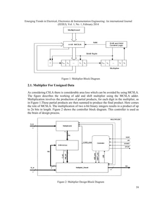
This document discusses the implementation of an unsigned multiplier using a modified carry select adder technique. It begins with an introduction to digital arithmetic operations like multiplication and addition. It then describes the proposed system, which uses a modified carry select adder based multiplier to reduce area over a traditional carry look ahead adder based multiplier, while maintaining similar delay times. The document provides details on the design of regular and modified square root carry select adders used in the multiplier. It discusses how replacing ripple carry adders with binary to excess-1 converters in the modified design can further reduce area and power consumption.


![Emerging Trends in Electrical, Electronics & Instrumentation Engineering: An international Journal
(EEIEJ), Vol. 1, No. 1, February 2014
66
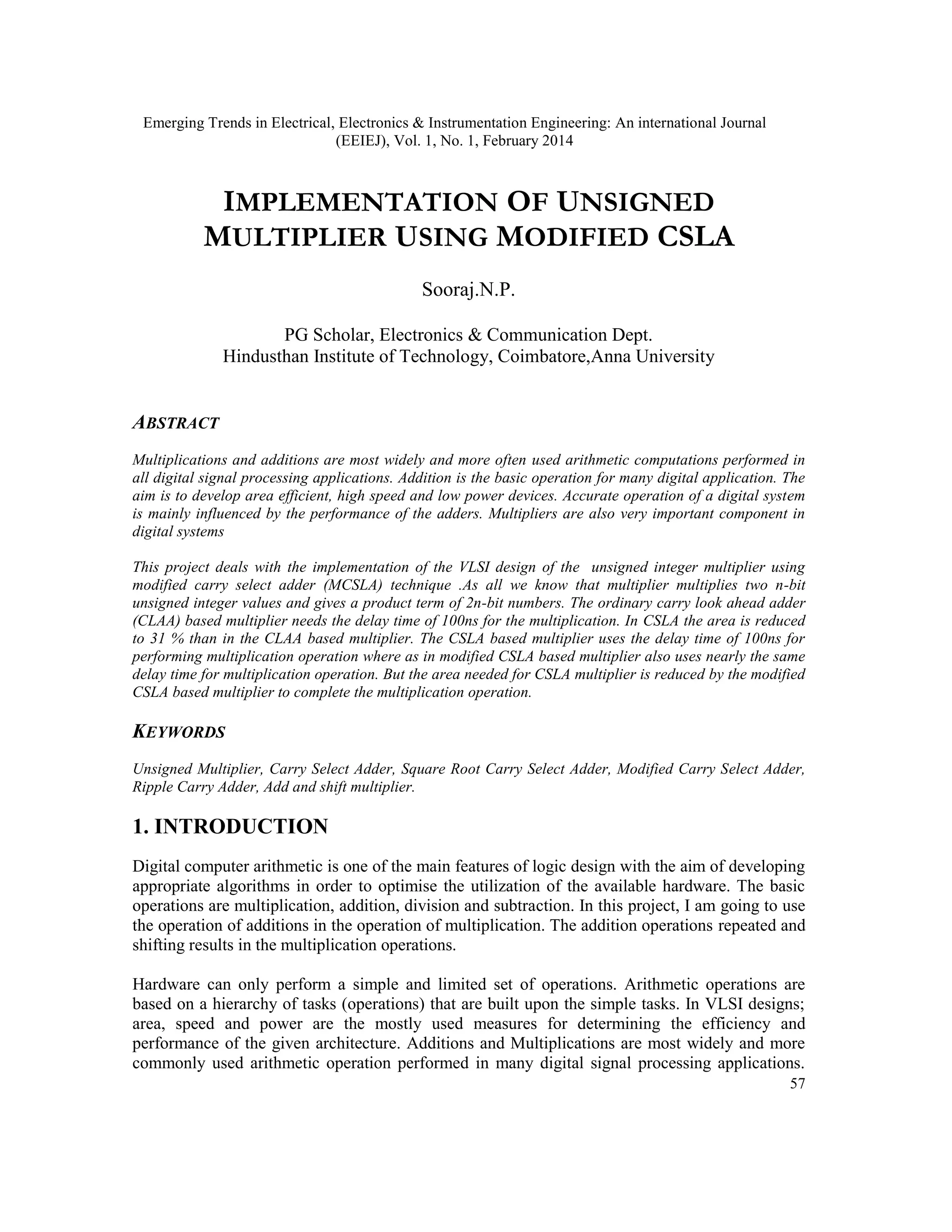
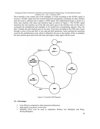
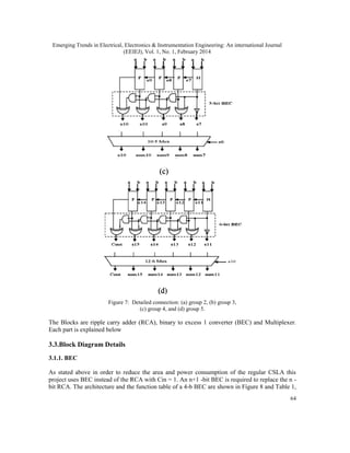
Figure 9: 4-b BEC with 8:4 MUX.
Table 1: Conversion table
B[3:0] X[3:0]
0000 0001
0001 0010
0010 0011
| |
1110 1111
1111 0000
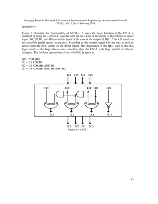
3.3.1. RCA
It is the well-known adder architecture. As shown in Figure 10 ripple carry adder is composed of
cascaded full adders for 4-bit adder. RCA can be constructed by cascading full adder blocks in
series. The carry out from one stage of full adder is fed to the carry-in of the next stage adder. ‘n’
full adders are required for an n-bit parallel adder. The dark line shows the carry flow from first
full adder to the last.](https://image.slidesharecdn.com/1114eeiej05-200130051132/85/IMPLEMENTATION-OF-UNSIGNED-MULTIPLIER-USING-MODIFIED-CSLA-10-320.jpg)
![Emerging Trends in Electrical, Electronics & Instrumentation Engineering: An international Journal
(EEIEJ), Vol. 1, No. 1, February 2014
69
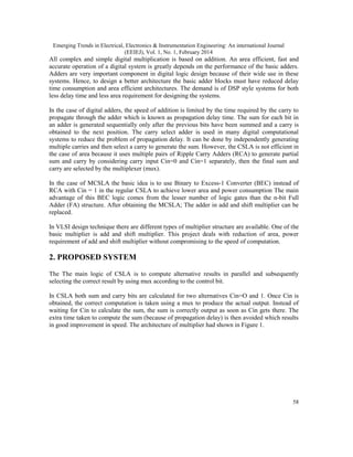
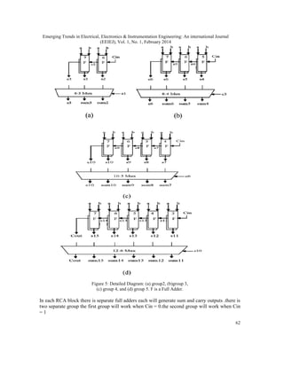
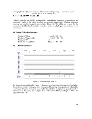
Figure 13: Simulated Output of Multiplier
5. CONCLUSIONS
Successfully achieved faster adder structure using the Modified Carry Select Adder structure.
With increasing word size, reduction of the delay increases; but the overhead of the area and
power constraints decreases. The MCSLA adder is used to construct efficient Add and Shift
multiplier. MCSLA structure also can be used to make Wallace tree multiplier and Baugh-
Wooley (BW) multiplier effectively. The proposed multipliers are energy efficient. The proposed
multiplier architecture can also be used to construct 32 bit, 64 bit and 128bit multiplier and
significant speed can be achieved without much area or power constraints; that is, the 128-bit
multiplier would be not only fast but also area, power, and energy efficient. The speed
improvements are significant. Proposed techniques also improve the performance of multipliers.
These design techniques can be implemented with all type of parallel multipliers of bit size higher
than 16-b to achieve optimum performance without significant area and power constraints.
ACKNOWLEDGMENT
I would like to thank the Department of Electronics and Communication Engineering, HIT,
Coimbatore for providing laboratory facilities and opportunity for experimental setup.
REFERENCES
[1] Ramkumar, B. and Harish M Kittur,( 2012) “Low Power and Area Efficient Carry Select Adder”,
IEEE Transactions on Very Large Scale Integration (VLSI) Systems, pp.1-5.
[2] V.Vijayalakshmil, R.Seshadd, Dr.S.Ramakrishnan,(2013) Design and Implementation of 32 Bit
Unsigned Multiplier Using CLAA and CSLA 978-1-4673-5301-IEEE.
Emerging Trends in Electrical, Electronics & Instrumentation Engineering: An international Journal
(EEIEJ), Vol. 1, No. 1, February 2014
69
Figure 13: Simulated Output of Multiplier
5. CONCLUSIONS
Successfully achieved faster adder structure using the Modified Carry Select Adder structure.
With increasing word size, reduction of the delay increases; but the overhead of the area and
power constraints decreases. The MCSLA adder is used to construct efficient Add and Shift
multiplier. MCSLA structure also can be used to make Wallace tree multiplier and Baugh-
Wooley (BW) multiplier effectively. The proposed multipliers are energy efficient. The proposed
multiplier architecture can also be used to construct 32 bit, 64 bit and 128bit multiplier and
significant speed can be achieved without much area or power constraints; that is, the 128-bit
multiplier would be not only fast but also area, power, and energy efficient. The speed
improvements are significant. Proposed techniques also improve the performance of multipliers.
These design techniques can be implemented with all type of parallel multipliers of bit size higher
than 16-b to achieve optimum performance without significant area and power constraints.
ACKNOWLEDGMENT
I would like to thank the Department of Electronics and Communication Engineering, HIT,
Coimbatore for providing laboratory facilities and opportunity for experimental setup.
REFERENCES
[1] Ramkumar, B. and Harish M Kittur,( 2012) “Low Power and Area Efficient Carry Select Adder”,
IEEE Transactions on Very Large Scale Integration (VLSI) Systems, pp.1-5.
[2] V.Vijayalakshmil, R.Seshadd, Dr.S.Ramakrishnan,(2013) Design and Implementation of 32 Bit
Unsigned Multiplier Using CLAA and CSLA 978-1-4673-5301-IEEE.](https://image.slidesharecdn.com/1114eeiej05-200130051132/85/IMPLEMENTATION-OF-UNSIGNED-MULTIPLIER-USING-MODIFIED-CSLA-13-320.jpg)
![Emerging Trends in Electrical, Electronics & Instrumentation Engineering: An international Journal
(EEIEJ), Vol. 1, No. 1, February 2014
70
[3] He, Y. Chang, C. H. and Gu, J.( 2005) “An Area Efficient 64-Bit Square Root Carry-Select Adder for
Low Power Applications,” in Proc. IEEE Int. Symp. Circuits Syst., Vol.4, pp. 4082–4085.
[4] Padma Devi, AshimaGirdher and Balwinder Singh (1998)“Improved Carry Select Adder with
Reduced Area and Low Power Consumption,”International Journal of Computer Applications, Vol.3,
No.4, pp. 14-18.
[5] AkhileshTyagi, (1993)“A Reduced-Area Scheme for Carry-Select Adders,” IEEE Transactions on
Computers, Vol.42, No.10, pp.1163-1170.
[6] Edison A.J and C.S.Manikandababu (2012.)“An Efficient CSLA Architecture for VLSI Hardware
Implementation” International Journal for Mechanical and Industrial Engineering, Vol. 2. Issue 5.
[7] P.Sreenivasulu,.K.SrinivasaRao, Malla Reddy, and A.VinayBabu(2012) “Energy sand Area efficient
Carry Select Adder on a reconFigureurable Hardware” International Journal of Engineering Research
and Applications, Vol. 2, Issue 2, pp.436-440.
[8] Sarabdeep Singh and Dilip Kumar, (2011) “Design of Area and Power efficient Modified Carry
Select Adder” International Journal of Computer Applications (0975 – 8887) Volume 33– No.3.
[9] S. Brown and Z. Vranesic, (2005) Fundamentals of Digital Logic with VHDL Design, 2nd ed.,
McGraw-Hill Higher Education, USA,. ISBN:0072499389.
[10] P. C. H. Meier, R. A. Rutenbar and L. R. Carley(1996), "Exploring Multiplier Architecture and
Layout for low Power", CIC'96.
[11] HasanKrad and AwsYousi(2010)"Design and Implementation of a Fast Unsigned 32-bit Multiplier
Using VHDL".
[12] SreehariVeeramachaneni, Kirthi M, Krishna LingamneniAvinashSreekanth Reddy Puppala M.B.
Srinivas(2007), ‘Novel Architectures for High-Speed and Low-Power 3-2, 4:2and 5:2Compressors’,
20th International Conference o VLSI Design, Pp: 324-329.
[13] S. F. Hsiao, M. R. Jiang, and J. S. Yeh, (1998.)‘Design of high speed low-power 3:2counter and
4:2compresso for fast multipliers’, Electron. Lett, vol. 34, no. 4, Pp. 341–343.
[14] K. Prasad and K. K. Parhi, (2001)‘Low-power 4:2and 5:2compressors,’ in Proc. of the 35th Asilomar
Conf. on Signals, Systems and Computers, vol. 1, , Pp.129–133.
[15] Massimo Alioto and Gaetano (2002), ‘Analysis and Comparison on Full Adder Block in Submicron
Technology’, IEEE Transaction Very Large Scale Integration (VLSI) Systems, Vol 10, No. 6, Pp: 806
–823.
[16] Anantha P. Chandrakasan, Samuel Sheng and Rober W. Brodersen (1992), ‘Low-Power CMOS
Digital Design‘, IEEE Journal of Solid State Circuits, Vol.27, No. 4.
[17] P. S. Mohanty,( 2009.)"Design and Implementation of Faster and Low Power Multipliers", Bachelor
Thesis. National Institute of Technology, Rourkela.
Author
Mr. Sooraj.N.P. Pursuing M.E. in VLSI Design and Embedded Systems, from
Hindusthan Institute of Technology, Coimbatore under Anna University, Chennai. He
Received B.Tech degree from Kannur University in Electronics and Communication
Engineering in 2010.He is currently an intern in Nexegen Technologies. He got many
prizes for the event line follower. His interests include automation, low power design and
robotics.](https://image.slidesharecdn.com/1114eeiej05-200130051132/85/IMPLEMENTATION-OF-UNSIGNED-MULTIPLIER-USING-MODIFIED-CSLA-14-320.jpg)