Download to read offline
![Design & Implement an IP Core for Fast Addition using Quaternary Signed Digit Number System
(IJSRD/Vol. 2/Issue 08/2014/051)
All rights reserved by www.ijsrd.com 222
Design & Implement an IP Core for Fast Addition using Quaternary
Signed Digit Number System
Raja Lavudi1
R.Anil kumar2
J. Suresh3
R.Gopi Reddy4
1
M.Tech 2,4
Assistant Professor 3
Associate Professor
1,2,3
Department of Electronics and Communication Engineering
1,2,3
Jyothishmathi College of Engineering and Technology
Abstract— With the binary number system, the computation
speed is limited by formation and propagation of carry
especially as the number of bits increases. Using a
quaternary Signed Digit number system one may perform
carry free addition, borrow free subtraction and
multiplication. However the QSD number system requires a
different set of prime modulo based logic elements for each
arithmetic operation. A carry free arithmetic operation can
be achieved using a higher radix number system such as
Quaternary Signed Digit (QSD). In QSD, each digit can be
represented by a number from -3 to 3. Carry free addition
and other operations on a large number of digits such as 64,
128, or more can be implemented with constant delay and
less complexity. Design is simulated & synthesized using
Modelsim6.0, Microwind and Leonardo Spectrum.
Key words: QSD, Modelsim6.0, Microwind, Leonardo
Spectrum
I. INTRODUCTION
These high performance adders are essential since the
speed of the digital processor depends heavily on the speed
of the adders used is the system. Also, it serves as a
building block for synthesis of all other arithmetic
operations. Adders are most commonly used in various
electronic applications e.g. Digital signal processing in
which adders are used to perform various algorithms like
FIR, IIR etc. In past, the major challenge for VLSI designer
is to reduce area of chip by using efficient optimization
techniques. Then the next phase is to increase the speed of
operation to achieve fast calculations like, in today’s
microprocessors millions of instructions are performed per
second. Speed of operation is one of the major constraints
in designing DSP processors[11]. The redundancy
associated with signed-digit numbers offers the possibility
of carry free addition. The redundancy provided in signed-
digit representation allows for fast addition and subtraction
because the sum or difference digit is a function of only the
digits in two adjacent digit positions of the operands for a
radix greater than 2, and 3 adjacent digit positions for a
radix of 2. Thus, the add time for two redundant signed-
digit numbers is a constant independent of the word length
of the operands, which is the key to high speed
computation. The advantage of carry free addition offered
by QSD numbers is exploited in designing a fast adder
circuit. Additionally adder designed with QSD number
system has a regular layout which is suitable for VLSI
implementation which is the great advantage over the
RBSD adder. An Algorithm for design of QSD adder is
proposed. This algorithm is used to write the VHDL code
for QSD adders. VHDL codes for QSD adder is simulated
and synthesized and the timing report is generated. The
timing report gives the delay time produced by the adder
structure.
Binary signed-digit numbers are known to allow
limitedcarry propagation with a somewhat more complex
addition process requiring very large circuit for
implementation [4] [10]. A special higher radix-based
(quaternary) representation of binary signed-digit numbers
not only allows carry-free addition and borrow-free
subtraction but also offers other important advantages such
as simplicity in logic and higher storage density [15].
A. Theorem It offers the advantage of reduced
circuit complexity both in terms of transistor count and
interconnections. QSD number uses 25% less space than
BSD to store number [10] and it can be verified by the
theorem described as underQSD numbers save 25% storage
compared to BSD: To represent a numeric value N log 4N
number of QSD digits and 3 log 4N binary bits are required
while for the same log 2N BSD digits and 2 log 2N binary
bits are required in BSD representation. Ratio of number of
bits in QSD to BSD representation for an arbitrary number
N is,
So the proposed QSD adder is better than RBSD
adder in terms of number of gates, input connections and
delay though both perform addition within constant time.
Proposed design has the advantages of both parallelisms as
well as reduced gate complexity. The computation speed
and circuit complexity increases as the number of
computation steps decreases. A two step schemes appear to
be a prudent choice in terms of computation speed and
storage complexity. Quaternary is the base 4 redundant
number system. The degree of redundancy usually increases
with the increase of the radix [24]. The signed digit number
system allows us to implement parallel arithmetic by using
redundancy. QSD numbers are the SD numbers with the
digit set as:
II. DESIGN ALGORITHM OF QSD ADDER
In QSD number system carry propagation chain are
eliminated which reduce the computation time substantially,
thus enhancing the speed of the machine [31]. As range of
QSD number is from -3 to 3, the addition result of two QSD
numbers varies from -6 to +6 [30]. Table I depicts the output](https://image.slidesharecdn.com/ijsrdv2i8173-150923093045-lva1-app6892/85/Design-Implement-an-IP-Core-for-Fast-Addition-using-Quaternary-Signed-Digit-Number-System-1-320.jpg)
![Design & Implement an IP Core for Fast Addition using Quaternary Signed Digit Number System
(IJSRD/Vol. 2/Issue 08/2014/051)
All rights reserved by www.ijsrd.com 222
Design & Implement an IP Core for Fast Addition using Quaternary
Signed Digit Number System
Raja Lavudi1
R.Anil kumar2
J. Suresh3
R.Gopi Reddy4
1
M.Tech 2,4
Assistant Professor 3
Associate Professor
1,2,3
Department of Electronics and Communication Engineering
1,2,3
Jyothishmathi College of Engineering and Technology
Abstract— With the binary number system, the computation
speed is limited by formation and propagation of carry
especially as the number of bits increases. Using a
quaternary Signed Digit number system one may perform
carry free addition, borrow free subtraction and
multiplication. However the QSD number system requires a
different set of prime modulo based logic elements for each
arithmetic operation. A carry free arithmetic operation can
be achieved using a higher radix number system such as
Quaternary Signed Digit (QSD). In QSD, each digit can be
represented by a number from -3 to 3. Carry free addition
and other operations on a large number of digits such as 64,
128, or more can be implemented with constant delay and
less complexity. Design is simulated & synthesized using
Modelsim6.0, Microwind and Leonardo Spectrum.
Key words: QSD, Modelsim6.0, Microwind, Leonardo
Spectrum
I. INTRODUCTION
These high performance adders are essential since the
speed of the digital processor depends heavily on the speed
of the adders used is the system. Also, it serves as a
building block for synthesis of all other arithmetic
operations. Adders are most commonly used in various
electronic applications e.g. Digital signal processing in
which adders are used to perform various algorithms like
FIR, IIR etc. In past, the major challenge for VLSI designer
is to reduce area of chip by using efficient optimization
techniques. Then the next phase is to increase the speed of
operation to achieve fast calculations like, in today’s
microprocessors millions of instructions are performed per
second. Speed of operation is one of the major constraints
in designing DSP processors[11]. The redundancy
associated with signed-digit numbers offers the possibility
of carry free addition. The redundancy provided in signed-
digit representation allows for fast addition and subtraction
because the sum or difference digit is a function of only the
digits in two adjacent digit positions of the operands for a
radix greater than 2, and 3 adjacent digit positions for a
radix of 2. Thus, the add time for two redundant signed-
digit numbers is a constant independent of the word length
of the operands, which is the key to high speed
computation. The advantage of carry free addition offered
by QSD numbers is exploited in designing a fast adder
circuit. Additionally adder designed with QSD number
system has a regular layout which is suitable for VLSI
implementation which is the great advantage over the
RBSD adder. An Algorithm for design of QSD adder is
proposed. This algorithm is used to write the VHDL code
for QSD adders. VHDL codes for QSD adder is simulated
and synthesized and the timing report is generated. The
timing report gives the delay time produced by the adder
structure.
Binary signed-digit numbers are known to allow
limitedcarry propagation with a somewhat more complex
addition process requiring very large circuit for
implementation [4] [10]. A special higher radix-based
(quaternary) representation of binary signed-digit numbers
not only allows carry-free addition and borrow-free
subtraction but also offers other important advantages such
as simplicity in logic and higher storage density [15].
A. Theorem It offers the advantage of reduced
circuit complexity both in terms of transistor count and
interconnections. QSD number uses 25% less space than
BSD to store number [10] and it can be verified by the
theorem described as underQSD numbers save 25% storage
compared to BSD: To represent a numeric value N log 4N
number of QSD digits and 3 log 4N binary bits are required
while for the same log 2N BSD digits and 2 log 2N binary
bits are required in BSD representation. Ratio of number of
bits in QSD to BSD representation for an arbitrary number
N is,
So the proposed QSD adder is better than RBSD
adder in terms of number of gates, input connections and
delay though both perform addition within constant time.
Proposed design has the advantages of both parallelisms as
well as reduced gate complexity. The computation speed
and circuit complexity increases as the number of
computation steps decreases. A two step schemes appear to
be a prudent choice in terms of computation speed and
storage complexity. Quaternary is the base 4 redundant
number system. The degree of redundancy usually increases
with the increase of the radix [24]. The signed digit number
system allows us to implement parallel arithmetic by using
redundancy. QSD numbers are the SD numbers with the
digit set as:
II. DESIGN ALGORITHM OF QSD ADDER
In QSD number system carry propagation chain are
eliminated which reduce the computation time substantially,
thus enhancing the speed of the machine [31]. As range of
QSD number is from -3 to 3, the addition result of two QSD
numbers varies from -6 to +6 [30]. Table I depicts the output](https://image.slidesharecdn.com/ijsrdv2i8173-150923093045-lva1-app6892/75/Design-Implement-an-IP-Core-for-Fast-Addition-using-Quaternary-Signed-Digit-Number-System-1-2048.jpg)
![Design & Implement an IP Core for Fast Addition using Quaternary Signed Digit Number System
(IJSRD/Vol. 2/Issue 08/2014/051)
All rights reserved by www.ijsrd.com 223
for all possible combinations of two numbers. The decimal
numbers in the range of -3 to +3 are represented by one digit
QSD number. As the decimal number exceeds from this
range, more than one digit of QSD number is required. For
the addition result, which is in the range of -6 to +6, two
QSD digits are needed. In the two digits QSD result the LSB
digit represents the sum bit and the MSB digit represents the
carry bit. To prevent this carry bit to propagate from lower
digit position to higher digit position QSD number
representation is used [37]. QSD numbers allow redundancy
in the number representations. The same decimal number
can be represented in more than one QSD representations.
So we choose such QSD represented number which prevents
further rippling of carry. To perform carry free addition, the
addition of two QSD numbers can be done in two steps [4]:
Step 1: First step generates an intermediate carry and
intermediate sum from the input QSD digits i.e., addend and
augend. Step 2: Second step combines intermediate sum of
current digit with the intermediate carry of the lower
significant digit. So the addition of two QSD numbers is
done in two stages. First stage of adder generates
intermediate carry and intermediate sum from the input
digits. Second stage of adder adds the intermediate sum of
current digit with the intermediate carry of lower significant
digit. To remove the further rippling of carry there are two
rules to perform QSD addition in two steps: Rule 1: First
rule states that the magnitude of the intermediate sum must
be less than or equal to 2 i.e., it should be in the range of -2
to +2. Rule 2: Second rule states that the magnitude of the
intermediate carry must be less than or equal to 1 i.e., it
should be in the range of -1 to +1.
According to these two rules the intermediate sum
and intermediate carry from the first step QSD adder can
have the range of -6 to +6. But by exploiting the redundancy
feature of QSD numbers we choose such QSD represented
number which satisfies the above mentioned two rules.
When the second step QSD adder adds the intermediate sum
of current digit, which is in the range of -2 to +2, with the
intermediate carry of lower significant digit, which is in the
range of -1 to +1, the addition result cannot be greater than 3
i.e., it will be in the range of -3 to +3[]. The addition result
in this range can be represented by a single digit QSD
number; hence no further carry is required. In the step 1
QSD adder, the range of output is from -6 to +6 which can
be represented in the intermediate carry and sum in QSD
format as shown in table I. We can see in the first column of
TableI that some numbers have multiple representations, but
only those that meet the above defined two rules are chosen.
The chosen intermediate carry and intermediate sum are
listed in the last column of Table I as the QSD coded
number. This addition process can be well understood by
following examples:
Example: To perform QSD addition of two
numbers A = 107 and B = -233 (One number is positive and
one number is negative). First convert the decimal number
to their equivalent QSD representation:
From these examples it is clear that the QSD adder
design process will carry two stages for addition. The first
stage generates intermediate carry and sum according to the
defined rules. In the second stage the intermediate carry
from the lower significant digit is added to the intermediate
sum of current digit which results in carry free output. In
this step the current digit can always absorb the carry-in
from the lower digit.
III. Logic Design and Implementation Using Of Single
Digit Qsd Adder Unit
There are two steps involved in the carry-free addition. The
first step generates an intermediate carry and sum from the
addend and augend. The second step combines the
intermediate sum of the current digit with the carry of the
lower significant digit. To prevent carry from further
rippling, two rules are defined. The first rule states that the
magnitude of the intermediate sum must be less than or
equal to 2. The second rule states that the magnitude of the
carry must be less than or equal to 1. Consequently, the
magnitude of the second step output cannot be greater than 3
which can be represented by a single-digit QSD number;
hence no further carry is required. In step 1, all possible
input pairs of the addend and augend are considered. The
range of input numbers can vary from -3 to +3, so the
addition result will vary from -6 to +6 which needs two
QSD digits. The lower significant digit serves as sum and
most significant digit serves as carry. The generation of the](https://image.slidesharecdn.com/ijsrdv2i8173-150923093045-lva1-app6892/85/Design-Implement-an-IP-Core-for-Fast-Addition-using-Quaternary-Signed-Digit-Number-System-2-320.jpg)
![Design & Implement an IP Core for Fast Addition using Quaternary Signed Digit Number System
(IJSRD/Vol. 2/Issue 08/2014/051)
All rights reserved by www.ijsrd.com 224
carry can be avoided by mapping the two digits into a pair
of intermediate sum and intermediate carry such that the nth
intermediate sum and the (n-1)th intermediate carry never
form any carry generating pair (3,3), (3,2), (3,1), (3 , 3 ), (3,
2 ), (3,1). If we restrict the representation such that the
intermediate carry is limited to a maximum of 1, and the
intermediate sum is restricted to be less than 2, then the final
addition will become carry free. Both inputs and outputs can
be encoded in 3-bit 2’s complement binary number. The
mapping between the inputs, addend and augend, and the
outputs, the intermediate carry and sum are shown in binary
format in Table II. To remove the further carry propagation
the redundancy feature of QSD numbers is used. We restrict
the representation such that all the intermediate carries are
limited to a maximum of 1, and the intermediate sums are
restricted to be less than 3, then the final addition will
become carry free. The QSD representations according to
these rules are shown in Table 4.3 for the range of -6 to +6.
As the range of intermediate carry is from -1 to +1, it can be
represented in 2 bit binary number but we take the 3 bit
representation for the bit compatibility with the intermediate
sum. At the input side, the addend Ai is represented by 3
variable input as A2, A1, A0 and the augend Bi is
represented by 3 variable input as B2, B1, B0. At the output
side, the intermediate carry IC is represented by IC2, IC1,
IC0 and the intermediate sum IS is represented by IS2, IS1,
IS0. The six variable expressions for intermediate carry and
intermediate sum in terms of inputs (A2, A1, A0, B2, B1
and B0) can be derived from Table 4.3. So we get the six
output expressions for IC2, IC1, IC0, IS2, IS1 and IS0. As
the intermediate carry can be represented by only 2 bits, the
third appended bit IC2 is equal to IC1 so the expression for
both outputs will be the same[5].
The VHDL code for intermediate carry and sum
generator in step 1 adder, by taking the six inputs (A2, A1,
A0, B2, B1 and B0) and six outputs (IC2, IC1, IC0, IS2, IS1
and IS0), has been written. The VHDL code is compiled and
simulated using ModelSim software. The design is
synthesized on FPGA device xc9536xvPC44 in Xilinx
XC9500XV technology using Leonardo Spectrum from
Mentor Graphics. Using 6 variable K-map, the logic
equations specifying a minimal hardware realization for
generating the intermediate carry and intermediate sum are
derived. The minterms for the intermediate carry (IC2 , IC1,
IC0) are:
The final sum which is carry free is generated from
those outputs i.e. Intermediate carry (IC2, IC1, and IC0) and
Intermediate sum (IS2, IS1, and IS0). Therefore it has six
input and three output bits.
IV. THE CONVERSION BETWEEN THE INPUTS AND OUTPUTS
OF THE INTERMEDIATE CARRY AND INTERMEDIATE S
Addition operation for higher order digit does not
wait for the completion of addition operation of the
immediate lower order digit resulting in a parallel addition
of each individual pair of digits.](https://image.slidesharecdn.com/ijsrdv2i8173-150923093045-lva1-app6892/85/Design-Implement-an-IP-Core-for-Fast-Addition-using-Quaternary-Signed-Digit-Number-System-3-320.jpg)
![Design & Implement an IP Core for Fast Addition using Quaternary Signed Digit Number System
(IJSRD/Vol. 2/Issue 08/2014/051)
All rights reserved by www.ijsrd.com 226
VI. CONCLUSION
In the proposed design of Quaternary Signed Digit adder
using NAND-NAND implementation for single digit
addition, the dynamic power dissipation is 36.255W at
5GHz frequency. These circuits consume less energy and
less energy and power, and shows better performance. The
delay of the proposed design is 2ns.The design is simulated
using Modelsim 6.0 and synthesized using Leonardo
Spectrum LS2006a_59, power dissipation is obtained using
Microwind. Consequently this design is appropriate to be
applied for construction of a high performance
multiprocessor which consists of many processing elements.
REFERENCES
[1] A. Avizinis “signed digit number representation for
fast parallel arithmetic”, IRE Transactions on Elec.
Comp..Vol EC-10,pp 389- 400,sept-1961.
[2] A.A.S. Awwal and J.U. Ahmed, “fast carry free adder
design using QSD number system ,”proceedings of
the IEEE 1993 national aerospace and electronic
conference, vol 2,pp 1085-1090,1993.
[3] Behrooz perhami “generalized signed digit number
systems, a unifying frame work for redundant number
reperesentation “.IEEE transactions on computers,vol
39,no.1,pp.89-98,January 19990.
[4] O. Ishizuka, A. Ohta, K. Tannno, Z. Tang, D.
Handoko, “VLSI design of a quaternary multiplier
with direct generation of partial products,”
Proceedings of the 27th International Symposium on
Multiple-Valued Logic, pp. 169-174, 1997.
[5] A.A.S Awwal, Syed M. Munir, A.T.M. Shafiqul
Khalid, Howard E. Michel and O. N. Garcia,
“Multivalued Optical Parallel Computation Using An
Optical Programmable Logic Array”, Informatica,
vol. 24, No. 4, pp. 467-473, 2000.
[6] F. Kharbash and G. M. Chaudhry, “Reliable Binary
Signed Digit Number Adder Design”, IEEE
Computer Society Annual Symposium on VLSI, pp
479-484, 2007.
[7] John Moskal, Erdal Oruklu and Jafar Saniie, “Design
and Synthesis of a Carry-Free Signed-Digit Decimal
Adder”, IEEE International symposium on Circuits
and Systems, pp 1089-1092, 2007.
[8] Kai Hwang, “Computer Arithmetic Principles,
Architecture and Design”, ISBN 0-471-03496-7, John
Wiley & Sons, 1979.
[9] P. K. Dakhole, D.G. Wakde, “ Multi Digit Quaternary
adder on Programmable Device : Design and
verification”, International Conference on Electronic
Design, pp. 1-4, Dec 2008.
[10][10] Behrooz Parhami, “Carry-Free Addition of
Recoded Binary SignedDigit Numbers”, IEEE
Transactions on Computers, Vol. 37, No. 11, pp.
1470-1476, November 1988.
[11]Reena Rani, Neelam Sharma, L.K.Singh, “FPGA
Implementation of Fast Adders using Quaternary
Signed Digit Number System” IEEE proceedings of
International Conference on Emerging Trends in
Electronic and Photonic Devices & Systems
(ELECTRO-2009), pp 132- 135, 2009.
[12]Reena Rani, Neelam Sharma, L.K.Singh, “Fast
Computing using Signed Digit Number System”
IEEE proceedings of International Conference on
Control, Automation, Communication And Energy
Conservation - 2009, 4th-6th June 2009.
[13]Reena Rani, L.K. Singh and Neelam Sharma, “A
Novel design of High Speed Adders Using
Quaternary Signed Digit Number System ”
International Journal of Computer and Network
Security(IJCNS), Vol. 2, No. 9, pp.62-66, September
2010.
[14]Vasundara Patel K S, K S Gurumurthy, “Design of
High Performance Quaternary Adders”, International
Journal of Computer Theory and Engineering, Vol.2,
No.6, pp. 944-952, December, 2010.](https://image.slidesharecdn.com/ijsrdv2i8173-150923093045-lva1-app6892/85/Design-Implement-an-IP-Core-for-Fast-Addition-using-Quaternary-Signed-Digit-Number-System-5-320.jpg)
![Design & Implement an IP Core for Fast Addition using Quaternary Signed Digit Number System
(IJSRD/Vol. 2/Issue 08/2014/051)
All rights reserved by www.ijsrd.com 227
[15]Ricardo Cunha, “quaternary lookup tables using
voltage mode CMOS logic design”, ISMVL 2007,
37th International Symposium on MultipleValued
Logic, pp.56-56, 2007, 13-16 May, 2007.
[16]Hirokatsu Shirahama and Takahiro Hanyu, “Design
of HighPerformance Quaternary Adders Based on
Output-Generator Sharing”, Proceedings of the 38th
International Symposium on Multiple Valued Logic,
pp. 8-13. 2008.
[17]Hirokatsu Shirahama and Takahiro Hanyu et.al,
“Design of a Processing Element Based on
Quaternary Differential Logic for a Multi-Core SIMD
Processor”, ISMVL, Proceedings of the 37th
International Symposium on Multiple-Valued Logic,
pp. 43, 2007.](https://image.slidesharecdn.com/ijsrdv2i8173-150923093045-lva1-app6892/85/Design-Implement-an-IP-Core-for-Fast-Addition-using-Quaternary-Signed-Digit-Number-System-6-320.jpg)

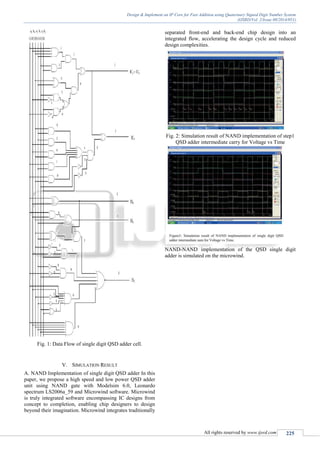
The document discusses the design and implementation of an IP core for fast addition using the quaternary signed digit (QSD) number system, which allows for carry-free arithmetic operations. By utilizing QSD, the proposed adder offers improved computation speed and reduced circuit complexity compared to binary signed-digit adders. The design is simulated and synthesized using various software tools, resulting in a power-efficient adder suitable for high-performance multiprocessors.