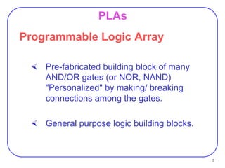
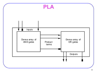
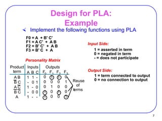
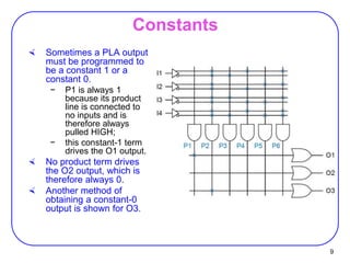
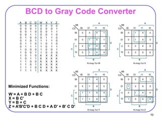
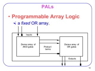
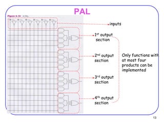
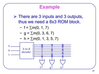
This document discusses programmable logic devices including PLA, PAL, and ROM. It provides examples of implementing logic functions using a PLA and converting between BCD and gray code using a PLA. ROM is described as a programmable logic device that can also be viewed as a memory, with the inputs serving as addresses and the outputs as stored data. An example is given of designing a BCD to 7-segment display controller using a ROM.


![26
ROM as Memory
0 1 1 0 1
1 0 0 0 0
2 1 0 0 1
3 0 0 1 0
4 0 0 0 0
5 1 0 0 0
6 0 0 1 1
7 0 1 0 0
Address
3 4
8x4 ROM
D0
D1
D2
D3
D4
D5
D6
D7
A2
A1
A0
A
B
C
F3F2F1F0
X XX
X
X
X
X
X
X
X
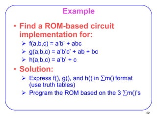
•Read Example: For input (A2,A1,A0) = 011, output is (F0,F1,F2,F3 ) =
0010.
•What are functions F3, F2 , F1 and F0 in terms of (A2, A1, A0)?
A[2:0] F[3:0]](https://image.slidesharecdn.com/palplarom-200206135328/85/PAL-25-320.jpg)