Lecture 13: Memoryand
Programmable Logic
Aby K George, ECE Department, Wayne State University
Syed M. Mahmud, Ph.D
ECE Department
Wayne State University
Introduction
• Memory unit:A device to which binary information is stored, and from
which information is retrieved when needed for processing.
• Two types of Memories
• Random Access Memory (RAM)
• Read Only Memory (ROM)
• RAM can perform read and write operations
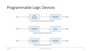
• ROM is a programmable logic device (PLD)
• Other types of PLDs
• Programmable Logic Array (PLA)
• Programmable Array Logic (PAL)
• Field Programmable Gate Array (FPGA)
Chapter 7 ECE 2610 – Digital Logic 1 3
4.
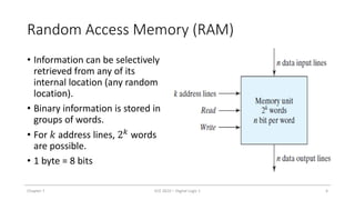
Random Access Memory(RAM)
• Information can be selectively
retrieved from any of its
internal location (any random
location).
• Binary information is stored in
groups of words.
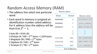
• For 𝑘 address lines, 2𝑘 words
are possible.
• 1 byte = 8 bits
Chapter 7 ECE 2610 – Digital Logic 1 4
5.
Random Access Memory(RAM)
• The address line select one particular
word.
• Each word in memory is assigned an
identification number called address.
For 𝑘 address lines the address will be
from 0 to 2𝑘 − 1.
Chapter 7 ECE 2610 – Digital Logic 1 5
1 byte (B) = 8 bits (b)
1 Kilobyte (K / KB) = 210 bytes = 1,024 bytes
1 Megabyte (M / MB) = 220 bytes
1 Gigabyte (G / GB) = 230
bytes
1 Terabyte (T / TB) = 240 bytes
1K X 16 Memory
6.
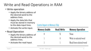
Write and ReadOperations in RAM
• Write operation
• Apply the binary address of
the desired word to the
address lines.
• Apply the data bits that
must be stored in memory
to the data input lines.
• Activate the write input.
• Read Operation
• Apply the binary address of
the desired word to the
address lines.
• Activate the read input.
Chapter 7 ECE 2610 – Digital Logic 1 6
7.
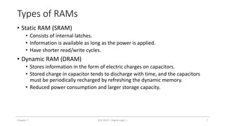
Types of RAMs
•Static RAM (SRAM)
• Consists of internal latches.
• Information is available as long as the power is applied.
• Have shorter read/write cycles.
• Dynamic RAM (DRAM)
• Stores information in the form of electric charges on capacitors.
• Stored charge in capacitor tends to discharge with time, and the capacitors
must be periodically recharged by refreshing the dynamic memory.
• Reduced power consumption and larger storage capacity.
Chapter 7 ECE 2610 – Digital Logic 1 7
8.
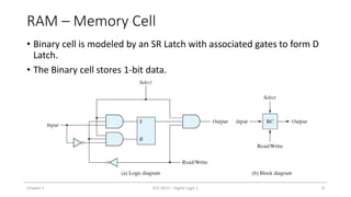
RAM – MemoryCell
• Binary cell is modeled by an SR Latch with associated gates to form D
Latch.
• The Binary cell stores 1-bit data.
Chapter 7 ECE 2610 – Digital Logic 1 8
9.
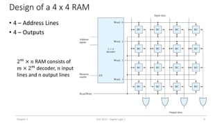
Design of a4 x 4 RAM
• 4 – Address Lines
• 4 – Outputs
Chapter 7 ECE 2610 – Digital Logic 1 9
2𝑚
× 𝑛 RAM consists of
𝑚 × 2𝑚 decoder, 𝑛 input
lines and n output lines
10.
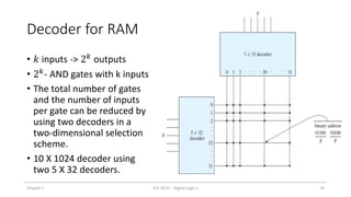
Decoder for RAM
•𝑘 inputs -> 2𝑘
outputs
• 2𝑘- AND gates with k inputs
• The total number of gates
and the number of inputs
per gate can be reduced by
using two decoders in a
two-dimensional selection
scheme.
• 10 X 1024 decoder using
two 5 X 32 decoders.
Chapter 7 ECE 2610 – Digital Logic 1 10
11.
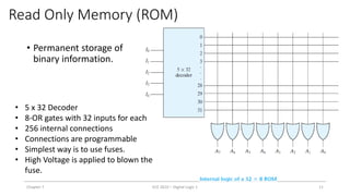
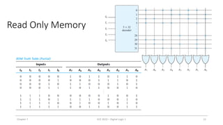
Read Only Memory(ROM)
• Permanent storage of
binary information.
Chapter 7 ECE 2610 – Digital Logic 1 11
• 5 x 32 Decoder
• 8-OR gates with 32 inputs for each
• 256 internal connections
• Connections are programmable
• Simplest way is to use fuses.
• High Voltage is applied to blown the
fuse.
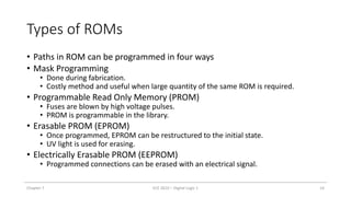
Types of ROMs
•Paths in ROM can be programmed in four ways
• Mask Programming
• Done during fabrication.
• Costly method and useful when large quantity of the same ROM is required.
• Programmable Read Only Memory (PROM)
• Fuses are blown by high voltage pulses.
• PROM is programmable in the library.
• Erasable PROM (EPROM)
• Once programmed, EPROM can be restructured to the initial state.
• UV light is used for erasing.
• Electrically Erasable PROM (EEPROM)
• Programmed connections can be erased with an electrical signal.
Chapter 7 ECE 2610 – Digital Logic 1 14
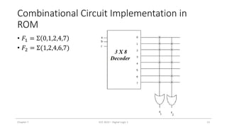
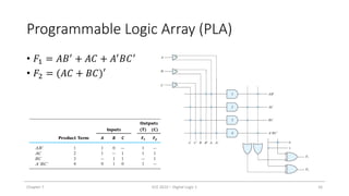
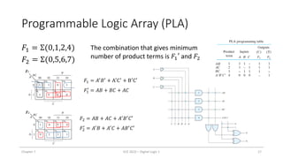
Programmable Logic Array(PLA)
𝐹1 = Σ(0,1,2,4)
𝐹2 = Σ(0,5,6,7)
Chapter 7 ECE 2610 – Digital Logic 1 17
𝐹1 = 𝐴′
𝐵′
+ A′
C′
+ B′
C′
𝐹1
′
= 𝐴𝐵 + 𝐵𝐶 + 𝐴𝐶
𝐹2 = 𝐴𝐵 + 𝐴𝐶 + 𝐴′
𝐵′
𝐶′
𝐹2
′
= 𝐴′𝐵 + 𝐴′𝐶 + 𝐴𝐵′𝐶′
The combination that gives minimum
number of product terms is 𝐹1′ and 𝐹2
18.
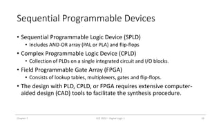
Sequential Programmable Devices
•Sequential Programmable Logic Device (SPLD)
• Includes AND-OR array (PAL or PLA) and flip-flops
• Complex Programmable Logic Device (CPLD)
• Collection of PLDs on a single integrated circuit and I/O blocks.
• Field Programmable Gate Array (FPGA)
• Consists of lookup tables, multiplexers, gates and flip-flops.
• The design with PLD, CPLD, or FPGA requires extensive computer-
aided design (CAD) tools to facilitate the synthesis procedure.
Chapter 7 ECE 2610 – Digital Logic 1 18
19.
Summary
• How toimplement a combinational function in a ROM?
• What is the difference between ROM, PLA and PAL?
• What are the different types of ROMs?
• How to implement a combinational function in a PLA?
• What are the common sequential programmable devices?
Chapter 7 ECE 2610 – Digital Logic 1 19
20.
Homework – 7
•7.1, 7.19, 7.20, 7.21
• Design a Full Adder using ROM and PLA
• Design a 5X2 RAM using D Flip-flop
Chapter 7 ECE 2610 – Digital Logic 1 20