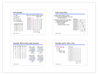
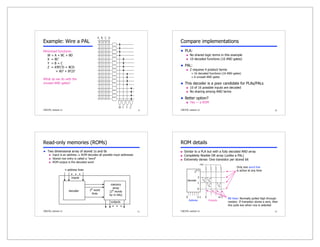
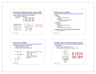
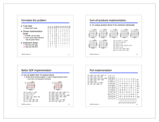
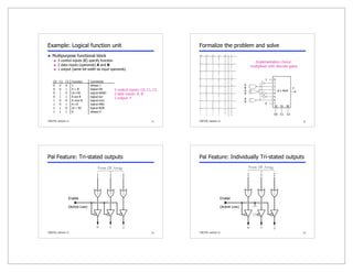
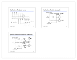
1
CSE370, Lecture 11
Overview
 Last lecture
 "Switching-network" logic blocks
 Multiplexers/selectors
 Demultiplexers/decoders
 Programmable logic devices (PLDs)
 Regular structures for 2-level logic
 Today
 PLDs
 PLAs
 PALs
 ROMs
 Tristates
 Design examples
2
CSE370, Lecture 11
• • •
• • •
inputs
outputs
product
terms
AND
array
OR
array
Programmable logic (PLAs & PALs )
 Concept: Large array of uncommitted AND/OR gates
 Actually NAND/NOR gates
 You program the array by making or breaking connections
 Programmable block for sum-of-products logic
3
CSE370, Lecture 11
Programming the wire connections
 Fuse: Comes connected; break unwanted connections
 Anti-fuse: Comes disconnected; make wanted connections
A B C
F1 F2 F3
F0
AB
B'C
AC'
B'C'
A
F0 = A + B'C'
F1 = AC' + AB
F2 = B'C' + AB
F3 = B'C + A
1
4
CSE370, Lecture 11
Short-hand notation
 Draw multiple wires as a single wire or bus
 × signifies a connection
After Programming
F0 F1
AB
A'B'
CD'
C'D
A B C D
Before Programming
F0 = AB + A'B'
F1 = CD' + C'D
5
CSE370, Lecture 11
A B C F1 F2 F3 F4 F5 F6
0 0 0 0 0 1 1 0 0
0 0 1 0 1 0 1 1 1
0 1 0 0 1 0 1 1 1
0 1 1 0 1 0 1 0 0
1 0 0 0 1 0 1 1 1
1 0 1 0 1 0 1 0 0
1 1 0 0 1 0 1 0 0
1 1 1 1 1 0 0 1 1
A'B'C'
A'B'C
A'BC'
A'BC
AB'C'
AB'C
ABC'
ABC
A B C
F1 F2 F3 F4 F5
F6
Think of as a memory-address decoder
Memory bits
PLA example
F1 = ABC
F2 = A + B + C
F3 = A' B' C'
F4 = A' + B' + C'
F5 = A xor B xor C
F6 = A xnor B xnor C
6
CSE370, Lecture 11
PLAs versus PALs
 We've been looking at PLAs
 Fully programmable AND / OR arrays
 Can share AND terms
 Programmable array logic (PAL)
 Programmable AND array
 OR array is prewired
 No sharing ANDs
 Cheaper and faster than PLAs
7
CSE370, Lecture 11
00 0 0 X 1
01 0 1 X 1
11 0 1 X X
10 0 1 X X
00 0 1 X 0
01 0 1 X 0
11 0 0 X X
10 0 0 X X
00 0 0 X 1
01 1 0 X 0
11 0 1 X X
10 1 0 X X
Example: BCD to Gray code converter
A B C D W X Y Z
0 0 0 0 0 0 0 0
0 0 0 1 0 0 0 1
0 0 1 0 0 0 1 1
0 0 1 1 0 0 1 0
0 1 0 0 0 1 1 0
0 1 0 1 1 1 1 0
0 1 1 0 1 0 1 0
0 1 1 1 1 0 1 1
1 0 0 0 1 0 0 1
1 0 0 1 1 0 0 0
1 0 1 0 X X X X
1 0 1 1 X X X X
1 1 0 0 X X X X
1 1 0 1 X X X X
1 1 1 0 X X X X
1 1 1 1 X X X X
A
D
AB
CD 00 01 11 10
C
B
K-map for W
A
D
AB
CD 00 01 11 10
C
B
A
D
00 0 1 X 0
01 0 1 X 0
11 1 1 X X
10 1 1 X X
AB
CD 00 01 11 10
C
B
A
D
AB
CD 00 01 11 10
C
B
K-map for X
K-map for Y K-map for Z
8
CSE370, Lecture 11
Example (con’t): Wire a PLA
A B C D
W X Y Z
Minimized functions:
W = A + BC + BD
X = BC'
Y = B + C
Z = A'B'C'D + BCD
+ AD' + B'CD'
9
CSE370, Lecture 11
Example: Wire a PAL
Minimized functions:
W = A + BC + BD
X = BC'
Y = B + C
Z = A'B'C'D + BCD
+ AD' + B'CD’
What do we do with the
unused AND gates?
10
CSE370, Lecture 11
Compare implementations
 PLA:
 No shared logic terms in this example
 10 decoded functions (10 AND gates)
 PAL:
 Z requires 4 product terms
 16 decoded functions (16 AND gates)
 6 unused AND gates
 This decoder is a poor candidate for PLAs/PALs
 10 of 16 possible inputs are decoded
 No sharing among AND terms
 Better option?
 Yes — a ROM
11
CSE370, Lecture 11
Read-only memories (ROMs)
 Two dimensional array of stored 1s and 0s
 Input is an address ⇒ ROM decodes all possible input addresses
 Stored row entry is called a "word"
 ROM output is the decoded word
inputs
outputs
n address lines
2n word
lines
decoder
• • •
• • •
memory
array
(2n words
by m bits)
12
CSE370, Lecture 11
ROM details
 Similar to a PLA but with a fully decoded AND array
 Completely flexible OR array (unlike a PAL)
 Extremely dense: One transistor per stored bit
decoder
0 n-1
Address
2
n-1
0
+5V
Bit lines: Normally pulled high through
resistor. If transistor stores a zero, then
line pulls low when row is selected
1
2
Only one word line
is active at any time
0 m-1
Outputs
13
CSE370, Lecture 11
A B C F0 F1 F2 F3
0 0 0 0 0 1 0
0 0 1 1 1 1 0
0 1 0 0 1 0 0
0 1 1 0 0 0 1
1 0 0 1 0 1 1
1 0 1 1 0 0 0
1 1 0 0 0 0 1
1 1 1 0 1 0 0
ROM
8 words x 4 bits/word
address outputs
A B C F0 F1 F2 F3
Two-level combinational logic using a ROM
 Use a ROM to directly store a truth table
 No need to minimize logic
 Example: F0 = A'B'C + AB'C' + AB'C
F1 = A'B'C + A'BC' + ABC
F2 = A'B'C' + A'B'C + AB'C'
F3 = A'BC + AB'C' + ABC'
You specify whether
to store 1 or 0 in each
location in the ROM
14
CSE370, Lecture 11
ROMs versus PLAs/PALs
 ROMs
 Benefits
 Quick to design, simple, dense
 Limitations
 Size doubles for each additional input
 Can't exploit don't cares
 PLAs/PALs
 Benefits
 Logic minimization reduces size
 Limitations
 PAL OR-plane has hard-wired fan-in
 Another answer: Field programmable gate arrays
 Learn about in 467
15
CSE370, Lecture 11
Loose end: Tristates
 Tristate buffers have a control input
 Enabled: Buffer works normally
 Disabled: Buffer output is disconnected
OUT
In1
In2
Sel
2:1 Tristate Mux module muxtri (In1,In2,Sel,OUT);
input In1,In2,Sel;
output OUT;
tri OUT;
bufif1 (OUT,In1,Sel);
bufif0 (OUT,In2,Sel);
endmodule
16
CSE370, Lecture 11
BCD to 7–segment
control-signal
decoder
c0 c1 c2 c3 c4 c5 c6
A B C D
c1
c5
c2
c4
c6
c0
c3
Example: BCD to 7-segment display controller
 The problem
 Input is a 4-bit BCD digit (A, B, C, D)
 Need signals to drive a display (7 outputs C0 – C6)
17
CSE370, Lecture 11
A B C D C0 C1 C2 C3 C4 C5 C6
0 0 0 0 1 1 1 1 1 1 0
0 0 0 1 0 1 1 0 0 0 0
0 0 1 0 1 1 0 1 1 0 1
0 0 1 1 1 1 1 1 0 0 1
0 1 0 0 0 1 1 0 0 1 1
0 1 0 1 1 0 1 1 0 1 1
0 1 1 0 1 0 1 1 1 1 1
0 1 1 1 1 1 1 0 0 0 0
1 0 0 0 1 1 1 1 1 1 1
1 0 0 1 1 1 1 0 0 1 1
1 0 1 – – – – – – – –
1 1 – – – – – – – – –
Formalize the problem
 Truth table
 Many don’t cares
 Choose implementation
target
 If ROM, we are done
 Don't cares imply PAL/PLA
may be good choice
 Implement design
 Minimize the logic
 Map into PAL/PLA
18
CSE370, Lecture 11
C0 = A + B D + C + B' D'
C1 = C' D' + C D + B'
C2 = B + C' + D
C3 = B' D' + C D' + B C' D + B' C
C4 = B' D' + C D'
C5 = A + C' D' + B D' + B C'
C6 = A + C D' + B C' + B' C
1 0 X 1
0 1 X 1
1 1 X X
1 1 X X
D
A
B
C
1 1 X 1
1 0 X 1
1 1 X X
1 0 X X
D
A
B
C
0 1 X 1
0 1 X 1
1 0 X X
1 1 X X
D
A
B
C
1 1 X 1
1 1 X 1
1 1 X X
0 1 X X
D
A
B
C
1 0 X 1
0 1 X 0
1 0 X X
1 1 X X
D
A
B
C
1 0 X 1
0 0 X 0
0 0 X X
1 1 X X
D
A
B
C
1 1 X 1
0 1 X 1
0 0 X X
0 1 X X
D
A
B
C
Sum-of-products implementation
 15 unique product terms if we minimize individually
19
CSE370, Lecture 11
C0 = BC'D + CD + B'D' + BCD' + A
C1 = B'D + C'D' + CD + B'D'
C2 = B'D + BC'D + C'D' + CD + BCD'
C3 = BC'D + B'D + B'D' + BCD'
C4 = B'D' + BCD'
C5 = BC'D + C'D' + A + BCD'
C6 = B'C + BC' + BCD' + A
C0 = A + BD + C + B'D'
C1 = C'D' + CD + B'
C2 = B + C' + D
C3 = B'D' + CD' + BC'D + B'C
C4 = B'D' + CD'
C5 = A + C'D' + BD' + BC'
C6 = A + CD' + BC' + B'C
C2 1 1 X 1
1 1 X 1
1 1 X X
0 1 X X
D
A
B
C
1 1 X 1
1 1 X 1
1 1 X X
0 1 X X
D
A
B
C
C2
Better SOP implementation
 Can do better than 15 product terms
 Share terms among outputs ⇒ only 9 unique product terms
 Each term not necessarily minimized
20
CSE370, Lecture 11
BC'
B'C
B'D
BC'D
C'D'
CD
B'D'
A
BCD'
A B C D
C0 C1 C2 C3 C4 C5 C6 C7
PLA implementation
C0 = BC'D + CD + B'D' + BCD' + A
C1 = B'D + C'D' + CD + B'D'
C2 = B'D + BC'D + C'D' + CD + BCD'
C3 = BC'D + B'D + B'D' + BCD'
C4 = B'D' + BCD'
C5 = BC'D + C'D' + A + BCD'
C6 = B'C + BC' + BCD' + A
21
CSE370, Lecture 11
C0 C1 C2 Function Comments
0 0 0 1 always 1
0 0 1 A + B logical OR
0 1 0 (A • B)' logical NAND
0 1 1 A xor B logical xor
1 0 0 A xnor B logical xnor
1 0 1 A • B logical AND
1 1 0 (A + B)' logical NOR
1 1 1 0 always 0
3 control inputs: C0, C1, C2
2 data inputs: A, B
1 output: F
Example: Logical function unit
 Multipurpose functional block
 3 control inputs (C) specify function
 2 data inputs (operands) A and B
 1 output (same bit-width as input operands)
22
CSE370, Lecture 11
Implementation choice:
multiplexer with discrete gates
C0 C1 C2 A B F
0 0 0 0 0 1
0 0 0 0 1 1
0 0 0 1 0 1
0 0 0 1 1 1
0 0 1 0 0 0
0 0 1 0 1 1
0 0 1 1 0 1
0 0 1 1 1 1
0 1 0 0 0 1
0 1 0 0 1 1
0 1 0 1 0 1
0 1 0 1 1 0
0 1 1 0 0 0
0 1 1 0 1 1
0 1 1 1 0 1
0 1 1 1 1 0
1 0 0 0 0 1
1 0 0 0 1 0
1 0 0 1 0 0
1 0 0 1 1 1
1 0 1 0 0 0
1 0 1 0 1 0
1 0 1 1 0 0
1 0 1 1 1 1
1 1 0 0 0 1
1 1 0 0 1 0
1 1 0 1 0 0
1 1 0 1 1 0
1 1 1 0 0 0
1 1 1 0 1 0
1 1 1 1 0 0
1 1 1 1 1 0
1
0
A
B
A
B
A
B
C2
C0 C1
0
1
2
3
4
5
6
7
S2
8:1 MUX
S1 S0
F
Formalize the problem and solve
23
CSE370, Lecture 11
Pal Feature: Tri-stated outputs
Enable
(Active Low)
24
CSE370, Lecture 11
Pal Feature: Individually Tri-stated outputs
Enable
(Active Low)
25
CSE370, Lecture 11
Pal Feature: Feedback terms
26
CSE370, Lecture 11
Pal Feature: Registered outputs
27
CSE370, Lecture 11
Pal Feature: Registers with bypass multiplexers

11-PLDs.pdf

  • 1.
    1 CSE370, Lecture 11 Overview Last lecture  "Switching-network" logic blocks  Multiplexers/selectors  Demultiplexers/decoders  Programmable logic devices (PLDs)  Regular structures for 2-level logic  Today  PLDs  PLAs  PALs  ROMs  Tristates  Design examples 2 CSE370, Lecture 11 • • • • • • inputs outputs product terms AND array OR array Programmable logic (PLAs & PALs )  Concept: Large array of uncommitted AND/OR gates  Actually NAND/NOR gates  You program the array by making or breaking connections  Programmable block for sum-of-products logic 3 CSE370, Lecture 11 Programming the wire connections  Fuse: Comes connected; break unwanted connections  Anti-fuse: Comes disconnected; make wanted connections A B C F1 F2 F3 F0 AB B'C AC' B'C' A F0 = A + B'C' F1 = AC' + AB F2 = B'C' + AB F3 = B'C + A 1 4 CSE370, Lecture 11 Short-hand notation  Draw multiple wires as a single wire or bus  × signifies a connection After Programming F0 F1 AB A'B' CD' C'D A B C D Before Programming F0 = AB + A'B' F1 = CD' + C'D
  • 2.
    5 CSE370, Lecture 11 AB C F1 F2 F3 F4 F5 F6 0 0 0 0 0 1 1 0 0 0 0 1 0 1 0 1 1 1 0 1 0 0 1 0 1 1 1 0 1 1 0 1 0 1 0 0 1 0 0 0 1 0 1 1 1 1 0 1 0 1 0 1 0 0 1 1 0 0 1 0 1 0 0 1 1 1 1 1 0 0 1 1 A'B'C' A'B'C A'BC' A'BC AB'C' AB'C ABC' ABC A B C F1 F2 F3 F4 F5 F6 Think of as a memory-address decoder Memory bits PLA example F1 = ABC F2 = A + B + C F3 = A' B' C' F4 = A' + B' + C' F5 = A xor B xor C F6 = A xnor B xnor C 6 CSE370, Lecture 11 PLAs versus PALs  We've been looking at PLAs  Fully programmable AND / OR arrays  Can share AND terms  Programmable array logic (PAL)  Programmable AND array  OR array is prewired  No sharing ANDs  Cheaper and faster than PLAs 7 CSE370, Lecture 11 00 0 0 X 1 01 0 1 X 1 11 0 1 X X 10 0 1 X X 00 0 1 X 0 01 0 1 X 0 11 0 0 X X 10 0 0 X X 00 0 0 X 1 01 1 0 X 0 11 0 1 X X 10 1 0 X X Example: BCD to Gray code converter A B C D W X Y Z 0 0 0 0 0 0 0 0 0 0 0 1 0 0 0 1 0 0 1 0 0 0 1 1 0 0 1 1 0 0 1 0 0 1 0 0 0 1 1 0 0 1 0 1 1 1 1 0 0 1 1 0 1 0 1 0 0 1 1 1 1 0 1 1 1 0 0 0 1 0 0 1 1 0 0 1 1 0 0 0 1 0 1 0 X X X X 1 0 1 1 X X X X 1 1 0 0 X X X X 1 1 0 1 X X X X 1 1 1 0 X X X X 1 1 1 1 X X X X A D AB CD 00 01 11 10 C B K-map for W A D AB CD 00 01 11 10 C B A D 00 0 1 X 0 01 0 1 X 0 11 1 1 X X 10 1 1 X X AB CD 00 01 11 10 C B A D AB CD 00 01 11 10 C B K-map for X K-map for Y K-map for Z 8 CSE370, Lecture 11 Example (con’t): Wire a PLA A B C D W X Y Z Minimized functions: W = A + BC + BD X = BC' Y = B + C Z = A'B'C'D + BCD + AD' + B'CD'
  • 3.
    9 CSE370, Lecture 11 Example:Wire a PAL Minimized functions: W = A + BC + BD X = BC' Y = B + C Z = A'B'C'D + BCD + AD' + B'CD’ What do we do with the unused AND gates? 10 CSE370, Lecture 11 Compare implementations  PLA:  No shared logic terms in this example  10 decoded functions (10 AND gates)  PAL:  Z requires 4 product terms  16 decoded functions (16 AND gates)  6 unused AND gates  This decoder is a poor candidate for PLAs/PALs  10 of 16 possible inputs are decoded  No sharing among AND terms  Better option?  Yes — a ROM 11 CSE370, Lecture 11 Read-only memories (ROMs)  Two dimensional array of stored 1s and 0s  Input is an address ⇒ ROM decodes all possible input addresses  Stored row entry is called a "word"  ROM output is the decoded word inputs outputs n address lines 2n word lines decoder • • • • • • memory array (2n words by m bits) 12 CSE370, Lecture 11 ROM details  Similar to a PLA but with a fully decoded AND array  Completely flexible OR array (unlike a PAL)  Extremely dense: One transistor per stored bit decoder 0 n-1 Address 2 n-1 0 +5V Bit lines: Normally pulled high through resistor. If transistor stores a zero, then line pulls low when row is selected 1 2 Only one word line is active at any time 0 m-1 Outputs
  • 4.
    13 CSE370, Lecture 11 AB C F0 F1 F2 F3 0 0 0 0 0 1 0 0 0 1 1 1 1 0 0 1 0 0 1 0 0 0 1 1 0 0 0 1 1 0 0 1 0 1 1 1 0 1 1 0 0 0 1 1 0 0 0 0 1 1 1 1 0 1 0 0 ROM 8 words x 4 bits/word address outputs A B C F0 F1 F2 F3 Two-level combinational logic using a ROM  Use a ROM to directly store a truth table  No need to minimize logic  Example: F0 = A'B'C + AB'C' + AB'C F1 = A'B'C + A'BC' + ABC F2 = A'B'C' + A'B'C + AB'C' F3 = A'BC + AB'C' + ABC' You specify whether to store 1 or 0 in each location in the ROM 14 CSE370, Lecture 11 ROMs versus PLAs/PALs  ROMs  Benefits  Quick to design, simple, dense  Limitations  Size doubles for each additional input  Can't exploit don't cares  PLAs/PALs  Benefits  Logic minimization reduces size  Limitations  PAL OR-plane has hard-wired fan-in  Another answer: Field programmable gate arrays  Learn about in 467 15 CSE370, Lecture 11 Loose end: Tristates  Tristate buffers have a control input  Enabled: Buffer works normally  Disabled: Buffer output is disconnected OUT In1 In2 Sel 2:1 Tristate Mux module muxtri (In1,In2,Sel,OUT); input In1,In2,Sel; output OUT; tri OUT; bufif1 (OUT,In1,Sel); bufif0 (OUT,In2,Sel); endmodule 16 CSE370, Lecture 11 BCD to 7–segment control-signal decoder c0 c1 c2 c3 c4 c5 c6 A B C D c1 c5 c2 c4 c6 c0 c3 Example: BCD to 7-segment display controller  The problem  Input is a 4-bit BCD digit (A, B, C, D)  Need signals to drive a display (7 outputs C0 – C6)
  • 5.
    17 CSE370, Lecture 11 AB C D C0 C1 C2 C3 C4 C5 C6 0 0 0 0 1 1 1 1 1 1 0 0 0 0 1 0 1 1 0 0 0 0 0 0 1 0 1 1 0 1 1 0 1 0 0 1 1 1 1 1 1 0 0 1 0 1 0 0 0 1 1 0 0 1 1 0 1 0 1 1 0 1 1 0 1 1 0 1 1 0 1 0 1 1 1 1 1 0 1 1 1 1 1 1 0 0 0 0 1 0 0 0 1 1 1 1 1 1 1 1 0 0 1 1 1 1 0 0 1 1 1 0 1 – – – – – – – – 1 1 – – – – – – – – – Formalize the problem  Truth table  Many don’t cares  Choose implementation target  If ROM, we are done  Don't cares imply PAL/PLA may be good choice  Implement design  Minimize the logic  Map into PAL/PLA 18 CSE370, Lecture 11 C0 = A + B D + C + B' D' C1 = C' D' + C D + B' C2 = B + C' + D C3 = B' D' + C D' + B C' D + B' C C4 = B' D' + C D' C5 = A + C' D' + B D' + B C' C6 = A + C D' + B C' + B' C 1 0 X 1 0 1 X 1 1 1 X X 1 1 X X D A B C 1 1 X 1 1 0 X 1 1 1 X X 1 0 X X D A B C 0 1 X 1 0 1 X 1 1 0 X X 1 1 X X D A B C 1 1 X 1 1 1 X 1 1 1 X X 0 1 X X D A B C 1 0 X 1 0 1 X 0 1 0 X X 1 1 X X D A B C 1 0 X 1 0 0 X 0 0 0 X X 1 1 X X D A B C 1 1 X 1 0 1 X 1 0 0 X X 0 1 X X D A B C Sum-of-products implementation  15 unique product terms if we minimize individually 19 CSE370, Lecture 11 C0 = BC'D + CD + B'D' + BCD' + A C1 = B'D + C'D' + CD + B'D' C2 = B'D + BC'D + C'D' + CD + BCD' C3 = BC'D + B'D + B'D' + BCD' C4 = B'D' + BCD' C5 = BC'D + C'D' + A + BCD' C6 = B'C + BC' + BCD' + A C0 = A + BD + C + B'D' C1 = C'D' + CD + B' C2 = B + C' + D C3 = B'D' + CD' + BC'D + B'C C4 = B'D' + CD' C5 = A + C'D' + BD' + BC' C6 = A + CD' + BC' + B'C C2 1 1 X 1 1 1 X 1 1 1 X X 0 1 X X D A B C 1 1 X 1 1 1 X 1 1 1 X X 0 1 X X D A B C C2 Better SOP implementation  Can do better than 15 product terms  Share terms among outputs ⇒ only 9 unique product terms  Each term not necessarily minimized 20 CSE370, Lecture 11 BC' B'C B'D BC'D C'D' CD B'D' A BCD' A B C D C0 C1 C2 C3 C4 C5 C6 C7 PLA implementation C0 = BC'D + CD + B'D' + BCD' + A C1 = B'D + C'D' + CD + B'D' C2 = B'D + BC'D + C'D' + CD + BCD' C3 = BC'D + B'D + B'D' + BCD' C4 = B'D' + BCD' C5 = BC'D + C'D' + A + BCD' C6 = B'C + BC' + BCD' + A
  • 6.
    21 CSE370, Lecture 11 C0C1 C2 Function Comments 0 0 0 1 always 1 0 0 1 A + B logical OR 0 1 0 (A • B)' logical NAND 0 1 1 A xor B logical xor 1 0 0 A xnor B logical xnor 1 0 1 A • B logical AND 1 1 0 (A + B)' logical NOR 1 1 1 0 always 0 3 control inputs: C0, C1, C2 2 data inputs: A, B 1 output: F Example: Logical function unit  Multipurpose functional block  3 control inputs (C) specify function  2 data inputs (operands) A and B  1 output (same bit-width as input operands) 22 CSE370, Lecture 11 Implementation choice: multiplexer with discrete gates C0 C1 C2 A B F 0 0 0 0 0 1 0 0 0 0 1 1 0 0 0 1 0 1 0 0 0 1 1 1 0 0 1 0 0 0 0 0 1 0 1 1 0 0 1 1 0 1 0 0 1 1 1 1 0 1 0 0 0 1 0 1 0 0 1 1 0 1 0 1 0 1 0 1 0 1 1 0 0 1 1 0 0 0 0 1 1 0 1 1 0 1 1 1 0 1 0 1 1 1 1 0 1 0 0 0 0 1 1 0 0 0 1 0 1 0 0 1 0 0 1 0 0 1 1 1 1 0 1 0 0 0 1 0 1 0 1 0 1 0 1 1 0 0 1 0 1 1 1 1 1 1 0 0 0 1 1 1 0 0 1 0 1 1 0 1 0 0 1 1 0 1 1 0 1 1 1 0 0 0 1 1 1 0 1 0 1 1 1 1 0 0 1 1 1 1 1 0 1 0 A B A B A B C2 C0 C1 0 1 2 3 4 5 6 7 S2 8:1 MUX S1 S0 F Formalize the problem and solve 23 CSE370, Lecture 11 Pal Feature: Tri-stated outputs Enable (Active Low) 24 CSE370, Lecture 11 Pal Feature: Individually Tri-stated outputs Enable (Active Low)
  • 7.
    25 CSE370, Lecture 11 PalFeature: Feedback terms 26 CSE370, Lecture 11 Pal Feature: Registered outputs 27 CSE370, Lecture 11 Pal Feature: Registers with bypass multiplexers