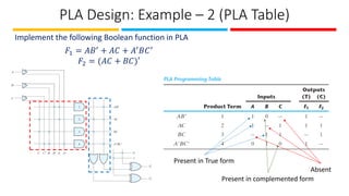
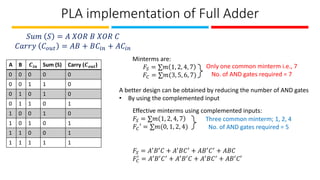
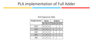
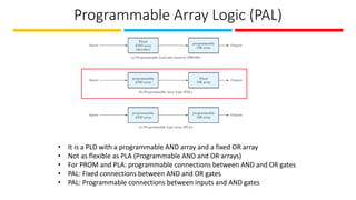
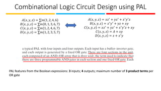
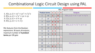
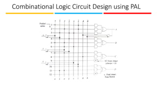
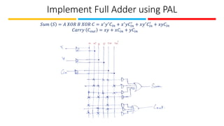
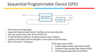
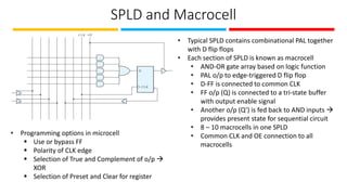
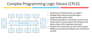
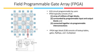
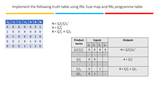
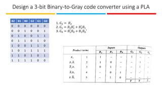
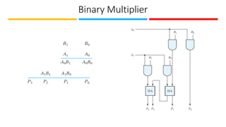
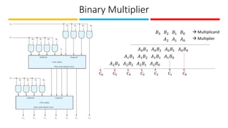
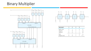
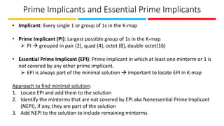
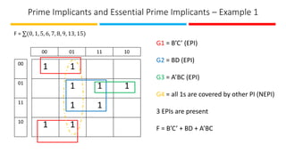
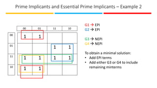
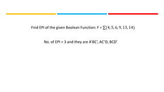
BITS Pilani, K K Birla Goa Campus
Souvik Ghosh
Department of Electrical and Electronics Engineering
Digital Electronics – Memory
Programmable Logic Array (PLA)
• PLA doesn’t generate all minterms
• Instead of a decoder (fixed AND gate array), tristate buffers are used in PLA
A’
A
PLA design: example - 1
Design a PLA device based on the given truth table.
A B C Y1 Y2
0 0 0 0 0
0 0 1 0 0
0 1 0 0 1
0 1 1 1 0
1 0 0 0 0
1 0 1 1 1
1 1 0 0 0
1 1 1 1 1
• Obtain the Boolean expression from the truth table:
𝑌1 = 𝐴𝐶 + 𝐵𝐶
𝑌2 = 𝐴𝐶 + 𝐴′𝐵𝐶′
• Implement the obtained Boolean expression in PLA
architecture
PLA Design: Example – 2
Implement the following Boolean function in PLA
𝐹1 = 𝐴𝐵′ + 𝐴𝐶 + 𝐴′𝐵𝐶′
𝐹2 = (𝐴𝐶 + 𝐵𝐶)′
• Fuse map of PLA can be explained with the Programming
table or PLA table
• Three sections in PLA table
• Section 1: List of product terms
• Section 2: Specifies the paths between inputs and AND
gates
• Section 3: specifies paths between AND and OR gates
• Outputs: can be True (T) or complemented (C)
• True o/p (T): another XOR i/p = 0
• Complement o/p (C): another XOR i/p = 1
PLA Design: Example – 2 (PLA Table)
Implement the following Boolean function in PLA
𝐹1 = 𝐴𝐵′ + 𝐴𝐶 + 𝐴′𝐵𝐶′
𝐹2 = (𝐴𝐶 + 𝐵𝐶)′
Absent
Present in True form
Present in complemented form
PLA implementation of Full Adder
𝑆𝑢𝑚 𝑆 = 𝐴 𝑋𝑂𝑅 𝐵 𝑋𝑂𝑅 𝐶
𝐶𝑎𝑟𝑟𝑦 𝐶𝑜𝑢𝑡 = 𝐴𝐵 + 𝐵𝐶𝑖𝑛 + 𝐴𝐶𝑖𝑛
A B 𝑪𝒊𝒏 Sum (S) Carry (𝑪𝒐𝒖𝒕)
0 0 0 0 0
0 0 1 1 0
0 1 0 1 0
0 1 1 0 1
1 0 0 1 0
1 0 1 0 1
1 1 0 0 1
1 1 1 1 1
Minterms are:
𝐹𝑆 = ∑𝑚 1, 2, 4, 7
𝐹𝐶 = ∑𝑚(3, 5, 6, 7)
Only one common minterm i.e., 7
No. of AND gates required = 7
A better design can be obtained by reducing the number of AND gates
• By using the complemented input
Effective minterms using complemented inputs:
𝐹𝑆 = ∑𝑚 1, 2, 4, 7
𝐹𝐶′ = ∑𝑚(0, 1, 2, 4)
𝐹𝑆 = 𝐴′𝐵′𝐶 + 𝐴′𝐵𝐶′ + 𝐴𝐵′𝐶′ + 𝐴𝐵𝐶
𝐹𝐶
′
= 𝐴′𝐵′𝐶′ + 𝐴′𝐵′𝐶 + 𝐴′𝐵𝐶′ + 𝐴𝐵′𝐶′
Three common minterm; 1, 2, 4
No. of AND gates required = 5
PLA implementation of Full Adder
Product terms Inputs Outputs
A B C 𝐹𝑆 (T) 𝐹𝐶 (𝐶)
A’B’C’ 0 0 0 - 1
A’B’C 0 0 1 1 1
A’BC’ 0 1 0 1 1
AB’C’ 1 0 0 1 1
ABC 1 1 1 1 -
PLA Programme Table
Programmable Array Logic (PAL)
• It is a PLD with a programmable AND array and a fixed OR array
• Not as flexible as PLA (Programmable AND and OR arrays)
• For PROM and PLA: programmable connections between AND and OR gates
• PAL: Fixed connections between AND and OR gates
• PAL: Programmable connections between inputs and AND gates
Combinational Logic Circuit Design using PAL
𝐴 𝑥, 𝑦, 𝑧 = ∑𝑚 1, 2, 4, 6
𝐵 𝑥, 𝑦, 𝑧 = ∑𝑚 0, 1, 3, 6, 7
𝐶 𝑥, 𝑦, 𝑧 = ∑𝑚 1, 2, 4, 6, 7
𝐷 𝑥, 𝑦, 𝑧 = ∑𝑚(1, 2, 3, 5, 7)
𝐴 𝑥, 𝑦, 𝑧 = 𝑥𝑧′ + 𝑦𝑧′ + 𝑥′𝑦′𝑧
𝐵 𝑥, 𝑦, 𝑧 = 𝑥′𝑦′ + 𝑦𝑧 + 𝑥𝑦
𝐶 𝑥, 𝑦, 𝑧 = 𝑥𝑧′ + 𝑦𝑧′ + 𝑥′𝑦′𝑧 + 𝑥𝑦
𝐶 𝑥, 𝑦, 𝑧 = 𝐴 + 𝑥𝑦
𝐷 𝑥, 𝑦, 𝑧 = 𝑧 + 𝑥′𝑦
PAL features from the Boolean expressions: 3 inputs; 4 outputs; maximum number of 3 product terms per
OR gate
Combinational Logic Circuit Design using PAL
1. 𝐴 𝑥, 𝑦, 𝑧 = 𝑥𝑧′ + 𝑦𝑧′ + 𝑥′𝑦′𝑧
2. 𝐵 𝑥, 𝑦, 𝑧 = 𝑥′𝑦′ + 𝑦𝑧 + 𝑥𝑦
3. 𝐶 𝑥, 𝑦, 𝑧 = 𝐴 + 𝑥𝑦
4. 𝐷 𝑥, 𝑦, 𝑧 = 𝑧 + 𝑥′
𝑦
PAL features from the Boolean
expressions: 3 inputs; 4 outputs;
maximum number of 3 product
terms per OR gate
PAL Program table
Product terms x y z A Outputs
1 xz’ 1 - 0 - 𝐴 𝑥, 𝑦, 𝑧 = 𝑥𝑧′
+ 𝑦𝑧′
+ 𝑥′
𝑦′
𝑧
2 yz’ - 1 0 -
3 x’y’z’ 0 0 0 -
4 x’y’ 0 0 - - 𝐵 𝑥, 𝑦, 𝑧 = 𝑥′𝑦′ + 𝑦𝑧 + 𝑥𝑦
5 yz - 1 1 -
6 xy 1 1 - -
7 xy 1 1 - - 𝐶 𝑥, 𝑦, 𝑧 = 𝐴 + 𝑥𝑦
8 A - - - 1
9 - - - - -
10 z - - 1 - 𝐷 𝑥, 𝑦, 𝑧 = 𝑧 + 𝑥′𝑦
11 x’y 0 1 - -
12 - - - - -
Combinational Logic Circuit Design using PAL
Implement Full Adder using PAL
𝑆𝑢𝑚 𝑆 = 𝐴 𝑋𝑂𝑅 𝐵 𝑋𝑂𝑅 𝐶 = 𝑥′𝑦′𝐶𝑖𝑛 + 𝑥′𝑦𝐶𝑖𝑛
′
+ 𝑥𝑦′𝐶𝑖𝑛
′
+ 𝑥𝑦𝐶𝑖𝑛
𝐶𝑎𝑟𝑟𝑦 𝐶𝑜𝑢𝑡 = 𝑥𝑦 + 𝑥𝐶𝑖𝑛 + 𝑦𝐶𝑖𝑛
Sequential Programmable Device (SPD)
• PLD contains only logic gates
• Sequential Programmable Device: Flip flops can be used externally
• PLD may contain PLA or PAL → o/p of PLD to FF
• FF o/p fed back to AND i/ps → provide present state condition
• outputs can be taken from the OR gates or the outputs of the flip-flops
• PAL or PLA with FF → Register
Three major types of SPD:
1. Simple Programmable Logic Device (SPLD)
2. Complex Programmable Logic Device (CPLD)
3. Field Programmable Gate Array (FPGA)
SPLD and Macrocell
• Typical SPLD contains combinational PAL together
with D flip flops
• Each section of SPLD is known as macrocell
• AND-OR gate array based on logic function
• PAL o/p to edge-triggered D flip flop
• D-FF is connected to common CLK
• FF o/p (Q) is connected to a tri-state buffer
with output enable signal
• Another o/p (Q’) is fed back to AND inputs →
provides present state for sequential circuit
• 8 – 10 macrocells in one SPLD
• Common CLK and OE connection to all
macrocells
• Programming options in microcell
▪ Use or bypass FF
▪ Polarity of CLK edge
▪ Selection of True and Complement of o/p →
XOR
▪ Selection of Preset and Clear for register
Complex Programming Logic Device (CPLD)
• Collection of individual PLDs in a single IC
• Multiple PLDs interconnected through a
programmable switch matrix
• I/O blocks provide the connections to the IC pins
• Switch matrix receives inputs from I/O block and
directs them to the individual macrocells
• Outputs from macrocells are sent to the outputs
• Different manufacturers follow to the architecture
of CPLD
Field Programmable Gate Array (FPGA)
• VLSI circuit programmable by users
• FPGA typically consists of an
(1) array of millions of logic blocks,
(2) surrounded by programmable input and output
blocks and
(3) connected together via programmable
interconnections
• FPGA logic block (CLB) consists of lookup tables,
gates, flipflops, and multiplexer
Implement the following truth table using PAL fuse map and PAL programme table
𝑰𝟎 𝑰𝟏 𝑰𝟐 𝑰𝟑 A B N
0 0 0 0 X X 1
1 X X X 0 0 0
0 1 X X 0 1 0
0 0 1 X 1 0 0
0 0 0 1 1 1 0
N = 𝐼0
′
𝐼1
′
𝐼2
′
𝐼3′
A = 𝐼0
′
𝐼1
′
B = 𝐼0
′
𝐼2
′
+ 𝐼0
′
𝐼1
Product
terms
Inputs Outputs
𝐼0 𝐼1 𝐼2 𝐼3
𝐼0
′
𝐼1
′
𝐼2
′
𝐼3
′
0 0 0 0 N = 𝐼0
′
𝐼1
′
𝐼2
′
𝐼3′
- - - - -
𝐼0
′
𝐼1
′
0 0 - - A = 𝐼0
′
𝐼1
′
- - - - -
𝐼𝑜
′
𝐼2 0 - 1 - B = 𝐼0
′
𝐼2
′
+ 𝐼0
′
𝐼1
𝐼0
′
𝐼1 0 1 - -
Design a 3-bit Binary-to-Gray code converter using a PLA
B2 B1 B0 G2 G1 G0
0 0 0 0 0 0
0 0 1 0 0 1
0 1 0 0 1 1
0 1 1 0 1 0
1 0 0 1 1 0
1 0 1 1 1 1
1 1 0 1 0 1
1 1 1 1 0 0
1. 𝐺2 = 𝐵2
2. 𝐺1 = 𝐵2𝐵1
′
+ 𝐵2
′
𝐵1
3. 𝐺0 = 𝐵1
′
𝐵0 + 𝐵1𝐵0′
Binary Multiplier
Binary Multiplier
𝐵3 𝐵2 𝐵1 𝐵0
𝐴2 𝐴1 𝐴0
→ Multiplicand
→ Multiplier
𝐴0𝐵3 𝐴0𝐵2 𝐴0𝐵1 𝐴0𝐵0
𝐴1𝐵3 𝐴1𝐵2 𝐴1𝐵1 𝐴1𝐵0
𝐴2𝐵3 𝐴2𝐵2 𝐴2𝐵1 𝐴2𝐵0
𝐶6 𝐶5 𝐶4 𝐶3 𝐶2 𝐶1 𝐶0
Binary Multiplier
Prime Implicants and Essential Prime Implicants
• Implicant: Every single 1 or group of 1s in the K-map
• Prime Implicant (PI): Largest possible group of 1s in the K-map
➢ PI → grouped in pair (2), quad (4), octet (8), double octet(16)
• Essential Prime Implicant (EPI): Prime implicant in which at least one minterm or 1 is
not covered by any other prime implicant.
➢ EPI is always part of the minimal solution → important to locate EPI in K-map
Approach to find minimal solution:
1. Locate EPI and add them to the solution
2. Identify the minterms that are not covered by EPI aka Nonessential Prime Implicant
(NEPI), if any, they are part of the solution
3. Add NEPI to the solution to include remaining minterms
Prime Implicants and Essential Prime Implicants – Example 1
F = ∑(0, 1, 5, 6, 7, 8, 9, 13, 15)
1 1
1 1 1
1 1
1 1
00 01 11 10
00
01
11
10
G1 = B’C’ (EPI)
G2 = BD (EPI)
G3 = A’BC (EPI)
G4 = all 1s are covered by other PI (NEPI)
3 EPIs are present
F = B’C’ + BD + A’BC
Prime Implicants and Essential Prime Implicants – Example 2
1 1
1 1
1 1 1 1
1 1
00 01 11 10
00
01
11
10
G1 → EPI
G2 → EPI
G3 → NEPI
G4 → NEPI
To obtain a minimal solution:
• Add EPI terms
• Add either G3 or G4 to include
remaining minterms
Find EPI of the given Boolean Function: F = ∑(4, 5, 6, 9, 13, 14)
No. of EPI = 3 and they are A’BC’, AC’D, BCD’
DD-F215-L-Memory_v2.pdfDIGITAL design bits

DD-F215-L-Memory_v2.pdfDIGITAL design bits

  • 1.
    BITS Pilani, KK Birla Goa Campus Souvik Ghosh Department of Electrical and Electronics Engineering Digital Electronics – Memory
  • 2.
    Programmable Logic Array(PLA) • PLA doesn’t generate all minterms • Instead of a decoder (fixed AND gate array), tristate buffers are used in PLA A’ A
  • 3.
    PLA design: example- 1 Design a PLA device based on the given truth table. A B C Y1 Y2 0 0 0 0 0 0 0 1 0 0 0 1 0 0 1 0 1 1 1 0 1 0 0 0 0 1 0 1 1 1 1 1 0 0 0 1 1 1 1 1 • Obtain the Boolean expression from the truth table: 𝑌1 = 𝐴𝐶 + 𝐵𝐶 𝑌2 = 𝐴𝐶 + 𝐴′𝐵𝐶′ • Implement the obtained Boolean expression in PLA architecture
  • 4.
    PLA Design: Example– 2 Implement the following Boolean function in PLA 𝐹1 = 𝐴𝐵′ + 𝐴𝐶 + 𝐴′𝐵𝐶′ 𝐹2 = (𝐴𝐶 + 𝐵𝐶)′ • Fuse map of PLA can be explained with the Programming table or PLA table • Three sections in PLA table • Section 1: List of product terms • Section 2: Specifies the paths between inputs and AND gates • Section 3: specifies paths between AND and OR gates • Outputs: can be True (T) or complemented (C) • True o/p (T): another XOR i/p = 0 • Complement o/p (C): another XOR i/p = 1
  • 5.
    PLA Design: Example– 2 (PLA Table) Implement the following Boolean function in PLA 𝐹1 = 𝐴𝐵′ + 𝐴𝐶 + 𝐴′𝐵𝐶′ 𝐹2 = (𝐴𝐶 + 𝐵𝐶)′ Absent Present in True form Present in complemented form
  • 6.
    PLA implementation ofFull Adder 𝑆𝑢𝑚 𝑆 = 𝐴 𝑋𝑂𝑅 𝐵 𝑋𝑂𝑅 𝐶 𝐶𝑎𝑟𝑟𝑦 𝐶𝑜𝑢𝑡 = 𝐴𝐵 + 𝐵𝐶𝑖𝑛 + 𝐴𝐶𝑖𝑛 A B 𝑪𝒊𝒏 Sum (S) Carry (𝑪𝒐𝒖𝒕) 0 0 0 0 0 0 0 1 1 0 0 1 0 1 0 0 1 1 0 1 1 0 0 1 0 1 0 1 0 1 1 1 0 0 1 1 1 1 1 1 Minterms are: 𝐹𝑆 = ∑𝑚 1, 2, 4, 7 𝐹𝐶 = ∑𝑚(3, 5, 6, 7) Only one common minterm i.e., 7 No. of AND gates required = 7 A better design can be obtained by reducing the number of AND gates • By using the complemented input Effective minterms using complemented inputs: 𝐹𝑆 = ∑𝑚 1, 2, 4, 7 𝐹𝐶′ = ∑𝑚(0, 1, 2, 4) 𝐹𝑆 = 𝐴′𝐵′𝐶 + 𝐴′𝐵𝐶′ + 𝐴𝐵′𝐶′ + 𝐴𝐵𝐶 𝐹𝐶 ′ = 𝐴′𝐵′𝐶′ + 𝐴′𝐵′𝐶 + 𝐴′𝐵𝐶′ + 𝐴𝐵′𝐶′ Three common minterm; 1, 2, 4 No. of AND gates required = 5
  • 7.
    PLA implementation ofFull Adder Product terms Inputs Outputs A B C 𝐹𝑆 (T) 𝐹𝐶 (𝐶) A’B’C’ 0 0 0 - 1 A’B’C 0 0 1 1 1 A’BC’ 0 1 0 1 1 AB’C’ 1 0 0 1 1 ABC 1 1 1 1 - PLA Programme Table
  • 8.
    Programmable Array Logic(PAL) • It is a PLD with a programmable AND array and a fixed OR array • Not as flexible as PLA (Programmable AND and OR arrays) • For PROM and PLA: programmable connections between AND and OR gates • PAL: Fixed connections between AND and OR gates • PAL: Programmable connections between inputs and AND gates
  • 9.
    Combinational Logic CircuitDesign using PAL 𝐴 𝑥, 𝑦, 𝑧 = ∑𝑚 1, 2, 4, 6 𝐵 𝑥, 𝑦, 𝑧 = ∑𝑚 0, 1, 3, 6, 7 𝐶 𝑥, 𝑦, 𝑧 = ∑𝑚 1, 2, 4, 6, 7 𝐷 𝑥, 𝑦, 𝑧 = ∑𝑚(1, 2, 3, 5, 7) 𝐴 𝑥, 𝑦, 𝑧 = 𝑥𝑧′ + 𝑦𝑧′ + 𝑥′𝑦′𝑧 𝐵 𝑥, 𝑦, 𝑧 = 𝑥′𝑦′ + 𝑦𝑧 + 𝑥𝑦 𝐶 𝑥, 𝑦, 𝑧 = 𝑥𝑧′ + 𝑦𝑧′ + 𝑥′𝑦′𝑧 + 𝑥𝑦 𝐶 𝑥, 𝑦, 𝑧 = 𝐴 + 𝑥𝑦 𝐷 𝑥, 𝑦, 𝑧 = 𝑧 + 𝑥′𝑦 PAL features from the Boolean expressions: 3 inputs; 4 outputs; maximum number of 3 product terms per OR gate
  • 10.
    Combinational Logic CircuitDesign using PAL 1. 𝐴 𝑥, 𝑦, 𝑧 = 𝑥𝑧′ + 𝑦𝑧′ + 𝑥′𝑦′𝑧 2. 𝐵 𝑥, 𝑦, 𝑧 = 𝑥′𝑦′ + 𝑦𝑧 + 𝑥𝑦 3. 𝐶 𝑥, 𝑦, 𝑧 = 𝐴 + 𝑥𝑦 4. 𝐷 𝑥, 𝑦, 𝑧 = 𝑧 + 𝑥′ 𝑦 PAL features from the Boolean expressions: 3 inputs; 4 outputs; maximum number of 3 product terms per OR gate PAL Program table Product terms x y z A Outputs 1 xz’ 1 - 0 - 𝐴 𝑥, 𝑦, 𝑧 = 𝑥𝑧′ + 𝑦𝑧′ + 𝑥′ 𝑦′ 𝑧 2 yz’ - 1 0 - 3 x’y’z’ 0 0 0 - 4 x’y’ 0 0 - - 𝐵 𝑥, 𝑦, 𝑧 = 𝑥′𝑦′ + 𝑦𝑧 + 𝑥𝑦 5 yz - 1 1 - 6 xy 1 1 - - 7 xy 1 1 - - 𝐶 𝑥, 𝑦, 𝑧 = 𝐴 + 𝑥𝑦 8 A - - - 1 9 - - - - - 10 z - - 1 - 𝐷 𝑥, 𝑦, 𝑧 = 𝑧 + 𝑥′𝑦 11 x’y 0 1 - - 12 - - - - -
  • 11.
  • 12.
    Implement Full Adderusing PAL 𝑆𝑢𝑚 𝑆 = 𝐴 𝑋𝑂𝑅 𝐵 𝑋𝑂𝑅 𝐶 = 𝑥′𝑦′𝐶𝑖𝑛 + 𝑥′𝑦𝐶𝑖𝑛 ′ + 𝑥𝑦′𝐶𝑖𝑛 ′ + 𝑥𝑦𝐶𝑖𝑛 𝐶𝑎𝑟𝑟𝑦 𝐶𝑜𝑢𝑡 = 𝑥𝑦 + 𝑥𝐶𝑖𝑛 + 𝑦𝐶𝑖𝑛
  • 13.
    Sequential Programmable Device(SPD) • PLD contains only logic gates • Sequential Programmable Device: Flip flops can be used externally • PLD may contain PLA or PAL → o/p of PLD to FF • FF o/p fed back to AND i/ps → provide present state condition • outputs can be taken from the OR gates or the outputs of the flip-flops • PAL or PLA with FF → Register Three major types of SPD: 1. Simple Programmable Logic Device (SPLD) 2. Complex Programmable Logic Device (CPLD) 3. Field Programmable Gate Array (FPGA)
  • 14.
    SPLD and Macrocell •Typical SPLD contains combinational PAL together with D flip flops • Each section of SPLD is known as macrocell • AND-OR gate array based on logic function • PAL o/p to edge-triggered D flip flop • D-FF is connected to common CLK • FF o/p (Q) is connected to a tri-state buffer with output enable signal • Another o/p (Q’) is fed back to AND inputs → provides present state for sequential circuit • 8 – 10 macrocells in one SPLD • Common CLK and OE connection to all macrocells • Programming options in microcell ▪ Use or bypass FF ▪ Polarity of CLK edge ▪ Selection of True and Complement of o/p → XOR ▪ Selection of Preset and Clear for register
  • 15.
    Complex Programming LogicDevice (CPLD) • Collection of individual PLDs in a single IC • Multiple PLDs interconnected through a programmable switch matrix • I/O blocks provide the connections to the IC pins • Switch matrix receives inputs from I/O block and directs them to the individual macrocells • Outputs from macrocells are sent to the outputs • Different manufacturers follow to the architecture of CPLD
  • 16.
    Field Programmable GateArray (FPGA) • VLSI circuit programmable by users • FPGA typically consists of an (1) array of millions of logic blocks, (2) surrounded by programmable input and output blocks and (3) connected together via programmable interconnections • FPGA logic block (CLB) consists of lookup tables, gates, flipflops, and multiplexer
  • 17.
    Implement the followingtruth table using PAL fuse map and PAL programme table 𝑰𝟎 𝑰𝟏 𝑰𝟐 𝑰𝟑 A B N 0 0 0 0 X X 1 1 X X X 0 0 0 0 1 X X 0 1 0 0 0 1 X 1 0 0 0 0 0 1 1 1 0 N = 𝐼0 ′ 𝐼1 ′ 𝐼2 ′ 𝐼3′ A = 𝐼0 ′ 𝐼1 ′ B = 𝐼0 ′ 𝐼2 ′ + 𝐼0 ′ 𝐼1 Product terms Inputs Outputs 𝐼0 𝐼1 𝐼2 𝐼3 𝐼0 ′ 𝐼1 ′ 𝐼2 ′ 𝐼3 ′ 0 0 0 0 N = 𝐼0 ′ 𝐼1 ′ 𝐼2 ′ 𝐼3′ - - - - - 𝐼0 ′ 𝐼1 ′ 0 0 - - A = 𝐼0 ′ 𝐼1 ′ - - - - - 𝐼𝑜 ′ 𝐼2 0 - 1 - B = 𝐼0 ′ 𝐼2 ′ + 𝐼0 ′ 𝐼1 𝐼0 ′ 𝐼1 0 1 - -
  • 18.
    Design a 3-bitBinary-to-Gray code converter using a PLA B2 B1 B0 G2 G1 G0 0 0 0 0 0 0 0 0 1 0 0 1 0 1 0 0 1 1 0 1 1 0 1 0 1 0 0 1 1 0 1 0 1 1 1 1 1 1 0 1 0 1 1 1 1 1 0 0 1. 𝐺2 = 𝐵2 2. 𝐺1 = 𝐵2𝐵1 ′ + 𝐵2 ′ 𝐵1 3. 𝐺0 = 𝐵1 ′ 𝐵0 + 𝐵1𝐵0′
  • 19.
  • 20.
    Binary Multiplier 𝐵3 𝐵2𝐵1 𝐵0 𝐴2 𝐴1 𝐴0 → Multiplicand → Multiplier 𝐴0𝐵3 𝐴0𝐵2 𝐴0𝐵1 𝐴0𝐵0 𝐴1𝐵3 𝐴1𝐵2 𝐴1𝐵1 𝐴1𝐵0 𝐴2𝐵3 𝐴2𝐵2 𝐴2𝐵1 𝐴2𝐵0 𝐶6 𝐶5 𝐶4 𝐶3 𝐶2 𝐶1 𝐶0
  • 21.
  • 22.
    Prime Implicants andEssential Prime Implicants • Implicant: Every single 1 or group of 1s in the K-map • Prime Implicant (PI): Largest possible group of 1s in the K-map ➢ PI → grouped in pair (2), quad (4), octet (8), double octet(16) • Essential Prime Implicant (EPI): Prime implicant in which at least one minterm or 1 is not covered by any other prime implicant. ➢ EPI is always part of the minimal solution → important to locate EPI in K-map Approach to find minimal solution: 1. Locate EPI and add them to the solution 2. Identify the minterms that are not covered by EPI aka Nonessential Prime Implicant (NEPI), if any, they are part of the solution 3. Add NEPI to the solution to include remaining minterms
  • 23.
    Prime Implicants andEssential Prime Implicants – Example 1 F = ∑(0, 1, 5, 6, 7, 8, 9, 13, 15) 1 1 1 1 1 1 1 1 1 00 01 11 10 00 01 11 10 G1 = B’C’ (EPI) G2 = BD (EPI) G3 = A’BC (EPI) G4 = all 1s are covered by other PI (NEPI) 3 EPIs are present F = B’C’ + BD + A’BC
  • 24.
    Prime Implicants andEssential Prime Implicants – Example 2 1 1 1 1 1 1 1 1 1 1 00 01 11 10 00 01 11 10 G1 → EPI G2 → EPI G3 → NEPI G4 → NEPI To obtain a minimal solution: • Add EPI terms • Add either G3 or G4 to include remaining minterms
  • 25.
    Find EPI ofthe given Boolean Function: F = ∑(4, 5, 6, 9, 13, 14) No. of EPI = 3 and they are A’BC’, AC’D, BCD’