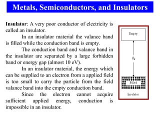
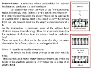
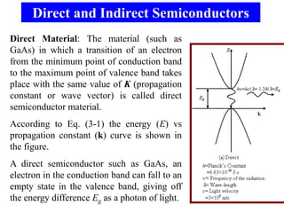
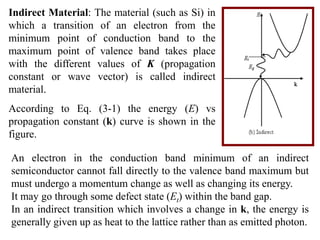
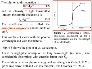
The document outlines the properties of insulators, semiconductors, and metals, detailing their conduction mechanisms and band structures. It explains intrinsic and extrinsic semiconductors, emphasizing the roles of doping and the effects of temperature on carrier concentrations. Additionally, it discusses Fermi-Dirac statistics in relation to carrier concentrations and the impact of Fermi levels on semiconductor behavior.
![For an energy E equal to the Fermi level energy EF, the occupation
probability is 1 1
f ( EF ) ( E F E F ) / kT
1 e 2
The significant of Fermi Level is that the probability of electron and
hole is 50 percent at the Fermi energy level. And, the Fermi function
is symmetrical about EF for all temperature; that is, the probability
f(EF +E) of electron that a state E above EF is filled is the same as
probability [1-f(EF-E)] of hole that a state E below EF is empty.
At 0K the distribution takes the
simple rectangular form shown in
Fig. 3-14.
With T=0K in the denominator of
the exponent, f(E) is 1/(1+0)=1
when the exponent is negative
(E<EF), and is 1/(1+)=0 when
the exponent is positive (E>EF).](https://image.slidesharecdn.com/opto-electronics-1-120508220004-phpapp01/85/Opto-electronics-12-320.jpg)
![This rectangular distribution implies that at 0K every available energy
state up to EF is filled with electrons, and all states above EF are empty.
At temperature higher than 0K, some probability exists for states above
the Fermi level to be filled.
At T=T1 in Fig. 3-14 there is
some probability f(E) that states
above EF are filled, and there is
a corresponding probability [1-
f(E)] that states below EF are
empty.
The symmetry of the
distribution of empty and filled
states about EF makes the Fermi
level a natural reference point
in calculations of electron and
hole concentration in
semiconductors.](https://image.slidesharecdn.com/opto-electronics-1-120508220004-phpapp01/85/Opto-electronics-13-320.jpg)
![For intrinsic material, the concentration of holes in
the valence band is equal to the concentration of
electrons in the conduction band.
Therefore, the Fermi level EF must lies at the middle
of the band gap.
Since f(E) is symmetrical
about EF, the electron
probability „tail‟ if f(E)
extending into the conduction
band of Fig. 3-15a is
symmetrical with the hole
probability tail [1-f(E)] in the
valence band.
Fig. 3-15(a) Intrinsic Material](https://image.slidesharecdn.com/opto-electronics-1-120508220004-phpapp01/85/Opto-electronics-14-320.jpg)
![In n-type material the Fermi level lies near Fig. 3.15(b) n-
the conduction band (Fig. 3-15b) such that type material
the value of f(E) for each energy level in the
conduction band increases as EF moves
closer to Ec.
Thus the energy difference (Ec- EF) gives
measure of n.
Fig. 3.15(c) p-
type material
In p-type material the Fermi level lies
near the valence band (Fig. 3-15c) such
that the [1- f(E)] tail value Ev is larger
than the f(E) tail above Ec.
The value of (EF-Ev) indicates how
strongly p-type the material is.](https://image.slidesharecdn.com/opto-electronics-1-120508220004-phpapp01/85/Opto-electronics-15-320.jpg)
![Electron and Hole Concentrations at Equilibrium
The concentration of electron and hole in the conduction band and
valance are
n0 E f ( E ) N ( E )dE (3.12a)
c
p0 [1 f ( E )] N ( E )dE
Ev
(3.12b)
where N(E)dE is the density of states (cm-3) in the energy range dE.
The subscript 0 used with the electron and hole concentration symbols
(n0, p0) indicates equilibrium conditions.
The number of electrons (holes) per unit volume in the energy range
dE is the product of the density of states and the probability of
occupancy f(E) [1-f(E)].
Thus the total electron (hole) concentration is the integral over the
entire conduction (valance) band as in Eq. (3.12).
The function N(E) is proportional to E(1/2), so the density of states in
the conduction (valance) band increases (decreases) with electron
(hole) energy.](https://image.slidesharecdn.com/opto-electronics-1-120508220004-phpapp01/85/Opto-electronics-17-320.jpg)
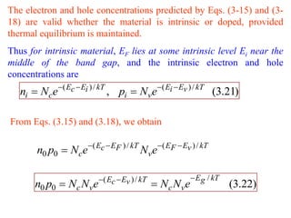
![Similarly, the probability of finding an empty state (hole) in the
valence band [1-f(E)] decreases rapidly below Ev, and most hole
occupy states near the top of the valence band.
This effect is demonstrated for intrinsic, n-type and p-type materials
in Fig. 3-16.
Fig. 3.16 (a) Concentration of electrons and holes in intrinsic material.](https://image.slidesharecdn.com/opto-electronics-1-120508220004-phpapp01/85/Opto-electronics-18-320.jpg)
![Steady State Carrier Generation
The thermal generation of EHPs is balanced by the recombination rate that means
[Eq. 3.7] g (T ) ar n2 ar n p (4.10)
i 0 0
If a steady state light is shone on the sample, an optical generation rate gop will be
added to the thermal generation, and the carrier concentration n and p will increase to
new steady sate values.
If n and p are the carrier concentrations which are departed from equilibrium:
g (T ) gop a r np a r (n0 n)( p0 p) (4.11)
For steady state recombination and no traping, n=p; thus Eq. (4.11) becomes
g (T ) gop a r n0 p0 a r [(n0 p0 )n n 2 ] (4.12)
Since g(T)==arn0p0 and neglecting the n2, we can rewrite Eq. (4.12) as
gop a r [(n0 p0 )n] (n / n ) (4.13)
1
where, n is the carrier life time.
a r (n0 p0 )
The excess carrier can be written as n p gop n (4.14)](https://image.slidesharecdn.com/opto-electronics-1-120508220004-phpapp01/85/Opto-electronics-30-320.jpg)