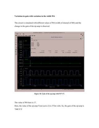
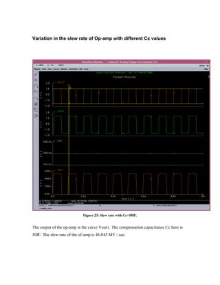
This document describes the design of an operational amplifier (op-amp) with specific gain and slew rate specifications. The design process involves choosing an architecture, then designing the transistor sizes and compensation network. An existing two-stage op-amp architecture is adapted. Transistor widths and lengths are calculated to meet the gain of 20,000 V/V and slew rate of 20 MV/sec. The schematic is drawn and simulated. The output is as expected but cannot drive the load, so an output buffer is added to minimize delay for larger loads.


![Block diagram
The general block diagram of an op-amp with an output buffer is shown below.
Figure 1 : Block diagram of two-stage op-amp with output buffer[1]
[1]The first stage of the op-amp is a differential amplifier. It has two inputs which are the
inverting and non-inverting voltages. The difference of these voltages is the output of the
differential stage. This is followed by the gain stage. This stage amplifies the voltage of
the differential amplifier. If the op-amp is intended to drive a small purely capacitive
load, which is the case in many switched capacitor or data conversion applications, the
output buffer is not used. [1]
[1] = CMOS Circuit Design. Layout, and Simulation By R. Jacob Baker.](https://image.slidesharecdn.com/07-200102100242/85/07-4-320.jpg)
![Design Strategy:
[2]The design process involves two distinct activities:
Architecture Design
• Find architecture already available and adapt it to present requirements
• Create a new architecture that can meet requirements
Component Design
• Design transistor sizes
• Design compensation network
If available architectures do not meet requirements, then an existing architecture must be
modified, or a new one designed. Once a satisfactory architecture has been obtained, then
devices and the compensation network must be designed.[2]
Circuit of the op-amp
Figure 2 : Circuit Diagram of two stage op-amp [2]
In this project, an architecture that is already available is used and is adapted to the
present requirements. For this architecture, devices and the compensation network is
designed.](https://image.slidesharecdn.com/07-200102100242/85/07-5-320.jpg)
![Design Procedure:
[2]In this project we aim to design an op-amp with a gain of 20000 V/V and a slew rate
of 20 MV/Sec.
The steps that are followed in designing the op-amp are:
1. The compensation capacitance is chosen to be at least 0.22 times the load capacitance
Cc > 0.22CL.
Here Cc is the compensation capacitance and CL is the load capacitance.
2. Determine the value for the “tail current” (I5).
I5 = SR .Cc
Here SR is the slew rate of the op-amp.
3. Design for S3 from the maximum input voltage specification.
S3 = ( Ι5 ÷ ( ) ( )[ ]( )2
minmax|03(max)3' VTIVTVinVDDK +−− ) 1≥
I5 is the drain current of M5, VDD is the positive supply voltage, Vin is the input voltage,
is the threshold voltage and K is the transconductance parameter (in saturation).VT
Also, S = (W/L).
4. Design for S1 (S2) to achieve the desired GB.
gm1 = GB. Cc S2 =⇒ 2
g m2 / K’2 I5
GB is the gain bandwidth and gm is the small signal transconductance from gate to
channel.
5. Design for S5 from the minimum input voltage. First calculate VDS5 (sat) then find S5.
VDS5 (sat) = Vin (min) − VSS − V−1I5/β Τ1 ( max)
S5 =2I5 /K'5 [VDS5 (sat)] 2
Where, β is the MOS transconductance parameter and VSS is the negative supply voltage.](https://image.slidesharecdn.com/07-200102100242/85/07-6-320.jpg)
![6. Find gm6 and S6.
gm6 = 2.2gm2(CL/Cc)
S6 = S3 (gm6 / gm3)
7. Calculate I6:
I6 = (S6/S4) I4 = (S6/S4)(I5/2)
8. Design S7 to achieve the desired current ratios between I5 and I6.
S7 = (I6/I5) S5
9. Simulate the circuit to check to see that all specifications are met.[2]
Design and Calculations for an op-amp with given specifications
Specifications:
Gain = 20,000 V/V Slew rate = 20 MV/sec
The positive supply voltage VDD = 1.5V
The negative supply voltage VSS = -1.5V
The maximum input voltage Vin (max) = 1.4V
The minimum input voltage Vin (min) = -0.97V
The load capacitance CL = 1pF and gain bandwidth = 2Π × 27.5 × 106
For 0.18 micrometer process:
The threshold voltages for CMOS = Vthn = Vthp =0.3V 10± %
The transconductance parameter (in saturation) for
NMOS = Kn = 288 μ A / V 2
PMOS = Kp = 77.84 μ A / V 2
[2] CMOS Analog Circuit Design By Phillip E. Allen and Douglas R. Holberg](https://image.slidesharecdn.com/07-200102100242/85/07-7-320.jpg)
2
minmax|03(max)3' VTIVTVinVDDK +−− )
⇒ S3 = (4.4 × 10 6−
÷ 77.84 10 ([1.5 – 1.4 – 0.345 + 0.255]) )× 6− 2
⇒ S3 5.≅
⇒ (W/L) 3 = (W/L) 4 = 5
4.) gm1 = GB. Cc
gm1 = 2 27.5 × 10 220 × 10 = 38.01Π × 6
× 15−
× 10 6−
⇒ gm1 = gm2 = 38.01 * 10 6−
⇒ S2 = m2
2
g / K’2 I5
⇒ S2 = 38.01 × 10 38.01 * 106−
× 6−
÷(288 × 10 6−
× 4.4 × 10 )6−
⇒ S2 1≅
⇒ (W/L)2= (W/L)1= 1
5.) VDS5 (sat) = Vin (min) − VSS − V−1I5/β Τ1 ( max)
⇒ VDS5 (sat) = -0.97– (-1.5) - 1288)10*4.4( 6
×÷−
- 0.345
⇒ VDS5 (sat) = 0.061V
S5 =2I5 /K'5 [VDS5 (sat)] 2
⇒S5= 2 × 4.4 × 10 6−
÷(288 × 10 6−
× 0.061 )2
⇒S5 ≅ 8
⇒ (W/L)5 = 8](https://image.slidesharecdn.com/07-200102100242/85/07-8-320.jpg)


![The Gain of the Op-amp
The circuit is now simulated with an inverting voltage of 1.4V and a non inverting
voltage of 1.40005 volts. This means that the difference of non-inverting and inverting
voltage is 5 × 10 V. The output of the op-amp is (Vout1). So, the gain of the op-amp is
[(5 10 ) / Vout1] V/V.
5−
× 5−
Figure 7: The gain of op-amp is observed from the waveform.
Here, the value of the op-amp Vout1 (curve 2) is 1.0309 volts. So, the gain of the op-amp
is 20,600 V/V. Notice that the output of the inverter is 1.5 volts and this value depends on
the value of the positive input voltage.](https://image.slidesharecdn.com/07-200102100242/85/07-15-320.jpg)