This document summarizes an experiment on characterizing the input and output properties of a bipolar junction transistor (BJT) and demonstrating its ability to amplify signals when biased in the active region. Key findings include:
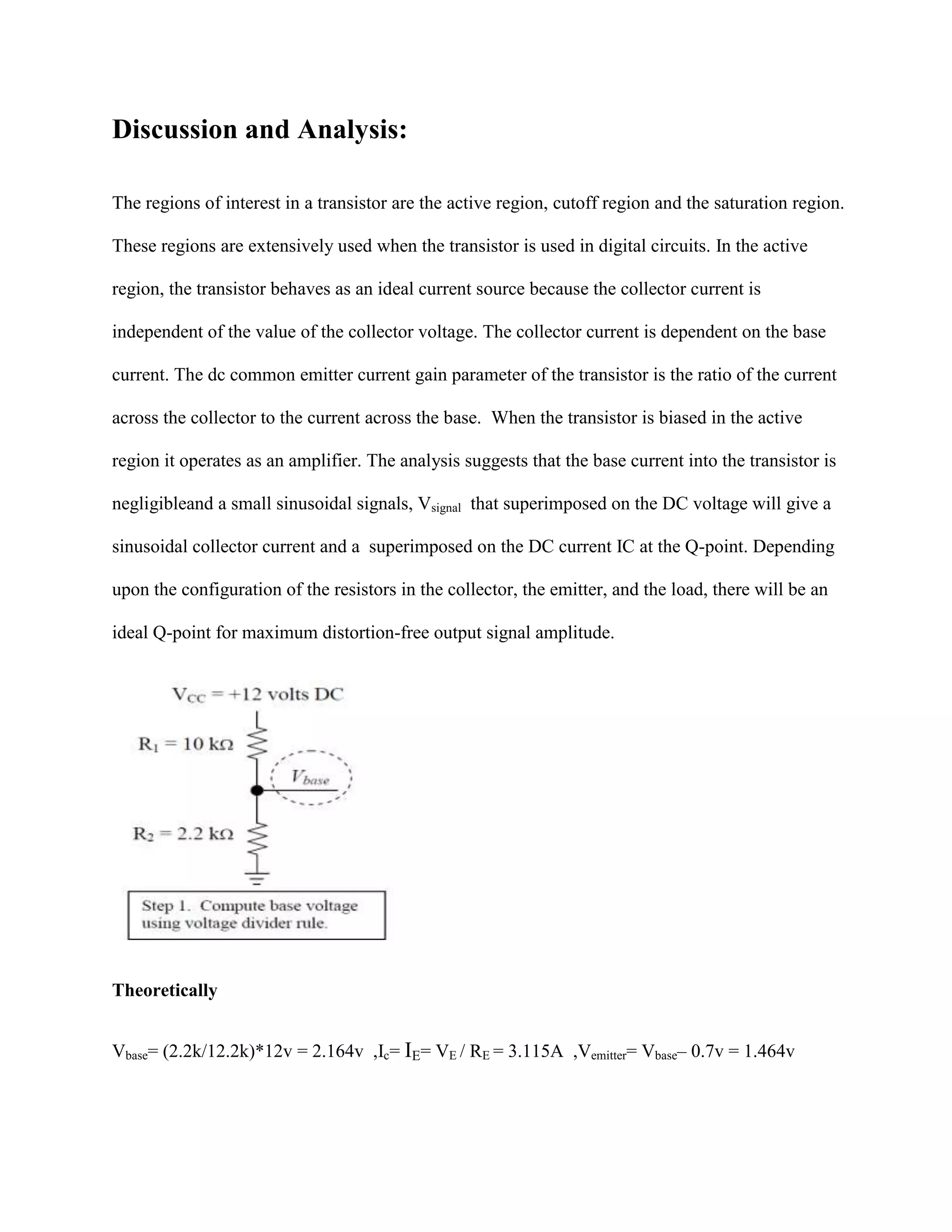
1) Measured voltages and currents matched predicted values closely, both from hand calculations and PSPICE simulations.
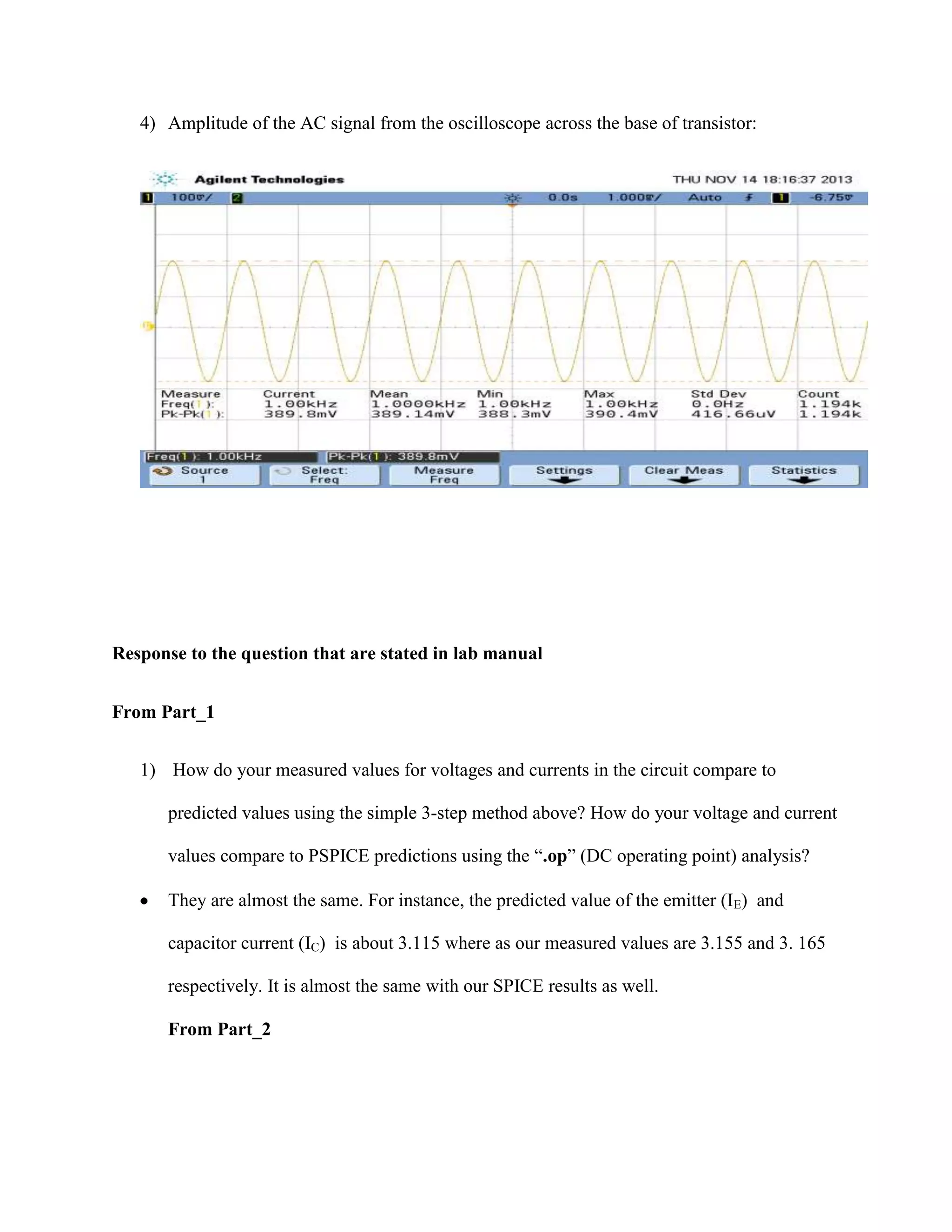
2) In the active region, a small AC input signal produced a larger AC output signal, demonstrating amplification. Measured gains matched predictions from an equivalent circuit model.
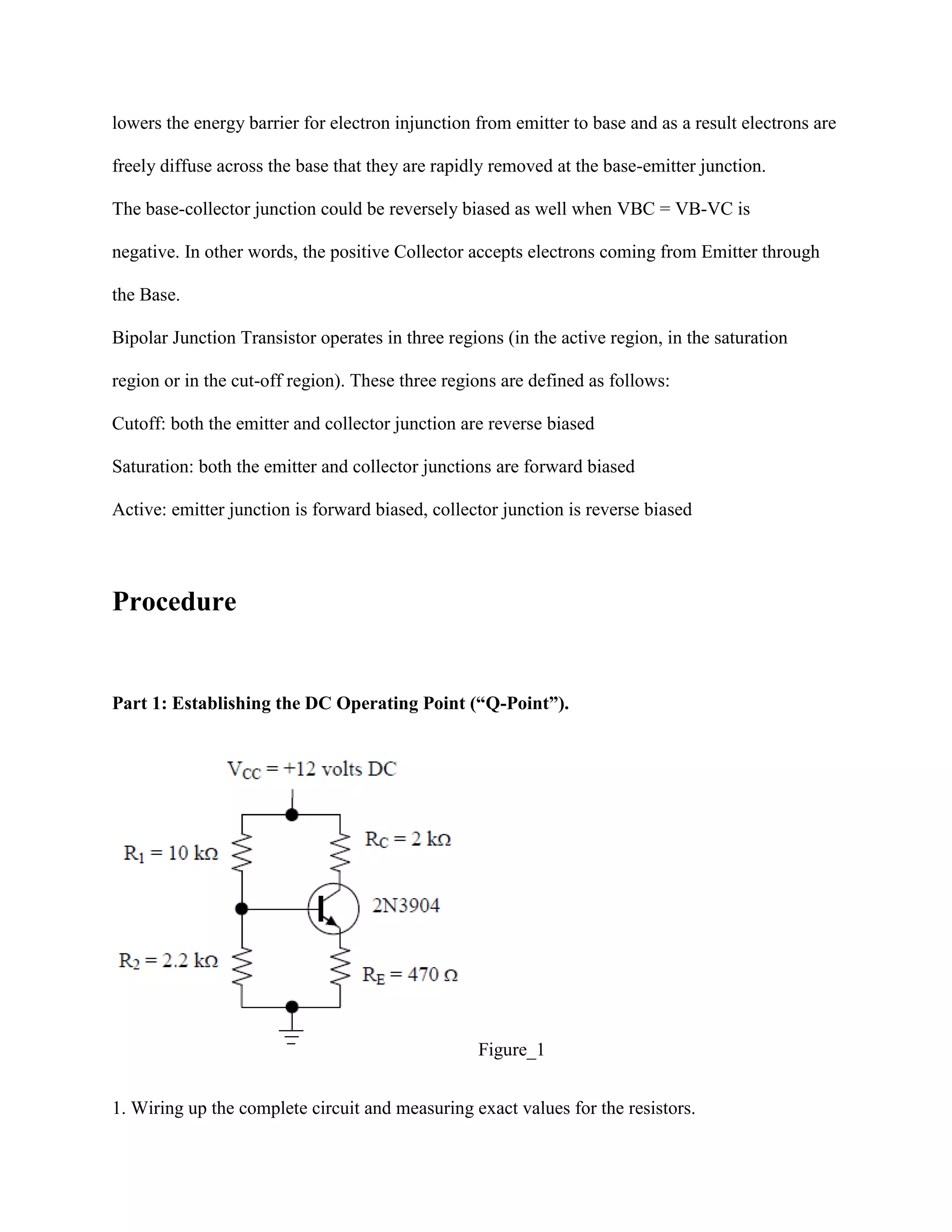
3) BJT regions of interest - active, cutoff, and saturation - were explored. In the active region the BJT acts as a current source, enabling its use as a signal amplifier.


![Multisim_simulation_project_3_^0_4[1]-2.pptx](https://cdn.slidesharecdn.com/ss_thumbnails/multisimsimulationproject3041-2-240418183400-1d9cbd89-thumbnail.jpg?width=640&height=640&fit=bounds)