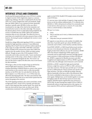
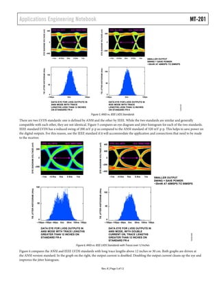
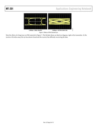
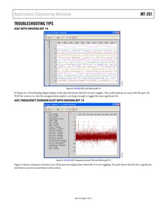
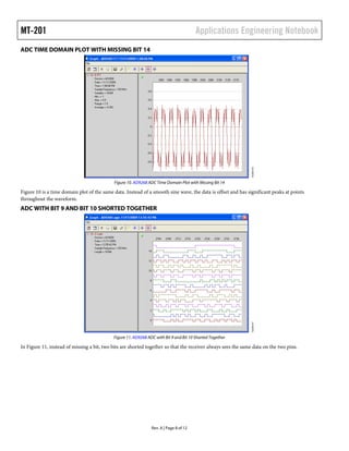
This document provides an overview of interfacing field programmable gate arrays (FPGAs) to analog-to-digital converter (ADC) outputs. It discusses various digital interface protocols and standards used by ADCs, including single data rate CMOS, double data rate CMOS, parallel low voltage differential signaling, serial LVDS, I2C, and JESD204. The document provides recommendations for minimizing noise when interfacing with CMOS outputs and examples of using series termination resistors. It also compares the ANSI and IEEE LVDS standards and shows the effects of trace length on signal integrity. Finally, it includes troubleshooting tips and examples of issues detectable from digital plots.
this presentation contains all sort of information regarding USCI(Universal Serial Communication Interface)
UART, SPI, I2C etc.
this will be very helpful to the people those who are planning or starting projects or want to get idea how devices interfaced.
CAN bus presentation covers all points in brief, at last please refer the references it really worth..
This was presented on 12-06-2017 in a Germany.
There was a 15 minutes time limit for presentation hence couldn't cover in detail
For further details please contact
10Gb/s DWDM XFP Transceiver Hot Pluggable, Duplex LC, +3.3V & +5V, 100GHz ITU...Allen He
SHXP-10G-Dxx-80 10Gb/s DWDM XFP transceiver, inter-converting the 10Gb/s serial electrical data stream with the 10Gb/s
optical signal, complies with XFP Multi-Source Agreement (MSA) Specification. It provides Digital diagnostics functions via a
2-wire serial interface. It supports the optical link length of 80km on single mode fiber.
HBM stands for high bandwidth memory and is a type of memory interface used in 3D-stacked DRAM (dynamic random access memory) in GPUs, as well as the server, machine-learning DSP , high-performance computing and networking and client space.
Practical steps for a successful project, Xiu Ji. PROFIBUS Seminar at MTC, Coventry, 2013.
Basics of PROFIBUS
Considerations at the design stage
Installation
Visual Checks
After reading this slide one can understand the serial data communication protocol RS-232 definition,standard,pin configuration,handshaking,advantages and disadvantages .
A conceptual study of social entrepreneurshipdeshwal852
Social entrepreneurship is a unique entrepreneurship which is totally driven by the societal problems. Business entrepreneurship focuses on wealth creation and is of interest because of its potential to fuel economic development whereas social entrepreneurship focuses on ‘making the world a better place’ and creating social capital. Social entrepreneurs are driven by an ethical obligation and desire to improve their communities and societies. In this back drop an attempt is made to highlight the importance, ethics and preparation of young social entrepreneurs. All the relevant data was collected
through review of available literature.
Discrete cosine transform (DCT) is a widely used tool in image and video compression applications. Recently, the high-throughput DCT designs have been adopted to fit the requirements of real-time application.
Operating the shifting and addition in parallel, an error-compensated adder-tree (ECAT) is proposed to deal with the truncation errors and to achieve low-error and high-throughput discrete cosine transform (DCT) design. Instead of the 12 bits used in previous works, 9-bit distributed arithmetic. DA-based DCT core with an error-compensated adder-tree (ECAT). The proposed ECAT operates shifting and addition in parallel by unrolling all the words required to be computed. Furthermore, the error-compensated circuit alleviates the truncation error for high accuracy design. Based on low-error ECAT, the DA-precision in this work is chosen to be 9 bits instead of the traditional 12 bits. Therefore, the hardware cost is reduced, and the speed is improved using the proposed ECAT.
The final thesis defense presentation for my master's project. The purpose of this thesis was to compare alternative wireless links for transfer of data from sink motes of remote wireless sensor networks to a central repository. A few different protocol stacks to be implemented in the WSN (Wireless Sensor Network) uplink gateway and along with them a few implementation environments based on open source software and low-power hardware were discussed. To facilitate measurements and experimental validation, some of the alternatives have been implemented. Experiments have been made using two of the amateur radio bands, the 144 MHz band (VHF) and the 433 MHz band (UHF). The parameters studied include throughput, range, power-requirements, portability and compatibility with standards.
Using different protocol stacks, different bands and sometimes different hardware 5 solutions were designed, implemented, tested and experimented with. Namely these solutions are called Radiotftp, Radiotftp_process, Radiotunnel, Soundmodem and APRX in this thesis.
After the implementation phase, there was an open-field experimentation to measure the aforementioned parameters. The tests were conducted in Riddarholmen, Stockholm of Sweden. These open-field experiments helped us obtain real-life measurements about power, throughput, stability etc. Experiments were conducted in a range of from a minimum of 2 meters to a maximum of 2.1 kilometers with some of the solutions.
In the end, some of these solutions proved themselves to be viable for the purpose of data communications for remote wireless sensor networks. Radiotftp gave the best throughput in both bands where it proved itself to be difficult to develop further applications. Radiotftp_process removed the necessity for a Linux running gateway machine but it was unable to work with faster baud rates. Radiotunnel opened up the path for a range of network applications to use radio links, but it also proved that it was unstable. On the other hand Soundmodem and APRX which were based on standard and open-source software proved that they were stable but rather slow. It was proven that every approach to problem has its advantages and disadvantages from different aspects such as throughput, range, power-requirements, portability and compatibility.
An Efficient Data Communication Using Conventional CodesIJERA Editor
The BER performance of conventional FFT-OFDM system is compared with DWT-OFDM system and DCT-OFDM system in an AWGN environment and Saleh-Valenzuela (SV) channel model at 60 GHz. Several wavelets such as Haar, Daubechies, Symlet, biorthogonal are considered. The BER is calculated for signaling format BPSK and the performance is analyzed at 60 GHz. Simulation results show that DCT based scheme yields the lowest average bit error rate. While out of all wavelet mother used Haar and Daubechies wavelet based scheme yields lower BER than FFT-OFDM for an AWGN channel. But it may include the implementation of forward error correction techniques such as convolution codes. An efficient channel estimation algorithm may be included for performance evaluation of DCT-OFDM and DWT- OFDM working at 60 GHz band. We introduce the Interfacing Techniques for Accessing data transfer data delivery. By using our approach we are increasing the efficiency of the data communication.
Giga bit per second Differential Scheme for High Speed InterconnectVLSICS Design
The performance of many digital systems today is limited by the interconnection bandwidth between chips. Although the processing performance of a single chip has increased dramatically since the inception of the integrated circuit technology, the communication bandwidth between chips has not enjoyed as much benefit. Most CMOS chips, when communicating off-chip, drive unterminated lines with full-swing CMOS drivers. Such full-swing CMOS interconnect ring-up the line, and hence has a bandwidth that is limited by the length of the line rather than the performance of the semiconductor technology. Thus, as VLSI technology scales, the pin bandwidth does not improve with the technology, but rather remains limited by board and cable geometry, making off-chip bandwidth an even more critical bottleneck. In order to increase the I/O Bandwidth, some efficient high speed signaling standard must be used which considers the line termination, signal integrity, power dissipation, noise immunity etc In this work, a transmitter has been developed for high speed offchip communication. It consists of low speed input buffer, serializer which converts parallel input data into serial data and a current mode driver which converts the voltage mode input signals into current over the transmission line. Output of 32 low speed input buffers is fed to two serializer, each serializer converting 16 bit parallel data into serial data stream. Output of two serializers is fed to LVDS current mode driver. The serial link technique used in this work is the time division multiplex (TDM) and point-to-point technique. It means that the low-speed parallel signals are transferred to the high-speed serial signal at the transmitter end and the high-speed serial signal is transferred to the low-speed parallel signals at the
receiver end. Serial link is the design of choice in any application where the cost of the communication channel is high and duplicating the links in large numbers is uneconomical.
– There are others : IS95 HDR, EDGE, etc.
» Direct Spread CDMA TDD
» Direct Spread CDMA FDD
» Multi-carrier CDMA FDD
Global 3G comprises of 3 modes :
– Marketed as Global 3G CDMA implying a single unified standard. In reality,
– Mostly dominated by Direct Sequence CDMA.
– Market is expected to be fragmented amongst several competing
IMT2000 guidelines defined by the ITU.
– Analog was 1G. GSM/IS95 were 2G. Next is 3G.
What is 3G ?
standards.
across the world.
Envisioned as a single Global standard allowing seamless roaming
Used interchangeably with IMT2000 although there are some specific
A loosely defined term referring to next generation wireless systems.
HIGH SPEED CONTINUOUS-TIME BANDPASS Σ∆ ADC FOR MIXED SIGNAL VLSI CHIPSVLSICS Design
With the unremitting progress in VLSI technology, there is a commensurate increase in performance demand on analog to digital converter and are now being applied to wideband communication systems. sigma Delta (Σ∆) converter is a popular technique for obtaining high resolution with relatively small bandwidth. Σ∆ ADCs which trade sampling speed for resolution can benefit from the speed advantages of nm-CMOS technologies. This paper compares various Band pass sigma Delta ADC architectures, both
continuous-time and discrete-time, in respect of power consumption and SNDR. Design of 2nd order multibit continuous time band pass Σ∆ modulator is discussed with the methods to resolve DAC non-idealities.
In wireless communications and data acquisition systems, there is more to consider when designing and implementing a complete solution beyond simply physically connecting a high speed analog module to an FPGA platform. Available hardware description language (HDL) components and software are critical to establishing an interface, which is necessary for practical system integration. This session starts with a top-level overview of various physical interfaces that are typically used and provides an in-depth focus on high speed serial JESD204B. Prototype HDL used for these types of boards is covered, along with the specific board components and how they are used to interface to high speed ADCs and DACs. Linux device drivers for the HDL components, as well as for the ADI components, are presented. This includes a short introduction into the Industrial I/O (IIO) framework, the benefits it offers, and how it can be used in end designs.
A Simulation of Wideband CDMA System on Digital Up/Down ConvertersEditor IJMTER
In this paper, I present FPGA implementation of a digital down converter (DDC) and
digital up converter (DUC) for a single carrier WCDMA system. The DDC and DUC is complex in
nature. The implementation of DDC is simple because it does not require mixers or filters. Xilinx
System Generator and Xilinx ISE are used to develop the hardware circuit for the FPGA. Both the
circuits are verified on the Spartan - 3 FPGA
High Speed Data Connectivity: More Than Hardware (Design Conference 2013)Analog Devices, Inc.
In wireless communications and data acquisition systems, there is more to consider when designing and implementing a complete solution beyond simply physically connecting a high speed analog module to an FPGA platform. Available hardware description language (HDL) components and software are critical to establish an interface, which is necessary for practical system integration. This session starts with a top-level overview of various physical interfaces that are typically used and provides an in-depth focus on high speed serial JESD204B. Prototype HDL used for these types of boards is covered, along with the specific board components and how they are used to interface to high speed ADCs and DACs. Linux device drivers for the HDL components as well as for the ADI components are presented. This includes a short introduction into the Industrial I/O (IIO) framework, the benefits it offers, and how it can be used in end designs.
Design of Low Power High Speed 4-Bit TIQ Based CMOS Flash ADCAman JanGra
The analog-to-digital converter (ADC) is an essential part of systemon-
chip (SoC) products because it bridges the gap between the analog physical
world and the digital logical world. In the digital domain, low power and low
voltage requirements are becoming more important issues as the channel length
of MOSFET shrinks below 0.25 sub-micron values. SoC trends force ADCs to
be integrated on the chip with other digital circuits. These trends present new
challenges in ADC circuit design. This paper investigates high speed, low
power, and low voltage CMOS flash ADCs for SoC applications.
This is an overview of the Analog Devices’ JESD204 Interface Framework, a system-level software package targeted at simplifying development by providing a performance optimized IP framework.
An Introduction to ADI’s Power components used in RF signal chains, with special treatment of high performance data converters, transceivers and PLL/VCOs.
An Introduction to ADI’s RF Switches and RF Attenuators including their key characteristics and how and where they should be used in the RF signal chain.
Digital isolation plays a key role in designing industrial motor control systems. This presentation takes you through why, where and how for isolation designs that optimize system performance while meeting the ever stringent safety and efficient standards. Analog Devices, Nicola O'Byrne at PCIM 2015
Isolation in gate drive is one critical area for designing efficient, safe and highly productive motor control systems. Learn how the latest ADI isolated gate drives can help you solve the design challenges. Analog Devices, Dara O'Sullivan PCIM 2015
When it comes to high performance signal chains, you need high performance power solutions. Noise sensitive
circuits such as analog-to-digital converters (ADCs), digital-to-analog converters (DACs), amplifiers, and phase
lock loops (PLLs)—as well as FPGAs—demand low noise power supplies that require specialized design
techniques. Engineers spend hours trying to figure out how to power these circuits without adding noise.
This presentation will focus on understanding various methods for not only approaching but meeting system
requirements. The session will introduce tested solutions and layout considerations that must be taken into
account when designing with switching regulators and low drop out (LDO) regulators.
This session provides insight into the operation of electric motor drive systems. Topics include electric motor operation and construction, motor control strategies, feedback sensors and circuits, power and isolation, and challenges of designing highly efficient motor control systems. A new high performance servo control FMC board will be introduced in the presentation, which provides an efficient motor control solution for different types of electric motors, addresses power and isolation challenges, and provides accurate measurement of motor feedback signals and increased control flexibility due to FPGA interfacing capabilities. The motor control hardware platform will be used to demonstrate rapid prototyping of motor control algorithms using Xilinx base platforms and the MathWorks development and simulation tools.
Finding the right combination of parts to create a signal chain can be a complex and daunting task, due to time demands, unfamiliarity with various technology areas, and the enormous amount of unproven solutions scattered across the Web. Signal Chain Designer is an intelligent selection and design tool that accesses verified product combinations and applications circuits, which can be customized or newly created according to user specifications. The Signal Chain Designer experience is supported by direct access to online EE design tools, evaluation hardware, software, documentation, and ADI Circuits from the Lab® reference circuits.
Sensors are the eyes, ears, and hands of electronic systems and allow them to capture the state of the environment. The capture and processing of sensor inputs is a delicate process that requires understanding of the signal details. Integration of sensor functions onto silicon has brought about improved performance, better signal handling, and lower total system cost. MEMS (microelectromechanical systems) sensors have opened up entire new areas and applications. In this session, the fundamental MEMS sensor concept of moving fingers that form a variable capacitor is covered, along with how it is turned into a usable motion signal. Adaptations for multiaccess sensing, rotational sensing, and even sound sensing, along with concepts of how these devices are tested and calibrated, are covered.
The industrial control market involves the monitoring and control aspects of both complex and simple processes. Common trends within the industry, notably the drive for increased efficiencies, better robustness, higher channel densities, and faster monitoring and control speeds, subsequently drive new technology advancements for semiconductor manufacturers. This session aims to give a broad overview of the system requirements for both field instruments (sensors/actuators) and control room (analog input/output) modules, and demonstrates a typical I/O module configuration with HART® (highway addressable remote transducer) connectivity.
This session combines the high speed analog signal chain from RF to baseband with FPGA-based digital signal processing for wireless communications. Topics include the high speed analog signal chain, direct conversion radio architecture, the high speed data converter interface, and FPGA-based digital signal processing for software-defined radio. The demo board uses the latest generation of Analog Devices’ high speed data converters, RF, and clocking devices, along with the Xilinx Zynq-7000 SoC. Other topics of discussion include the imperfections introduced by the modulator/demodulator with particular focus on the effect of temperature and frequency changes. In-factory and in-field algorithms that reduce the effect of these imperfections, with particular emphasis on the efficacy of in-factory set-and-forget algorithms, are examined.
Instrumentation: Test and Measurement Methods and Solutions - VE2013Analog Devices, Inc.
Tilt Measurement: Tilt measurement is fast becoming a fundamental analysis tool in many fields including automotive, industrial, and healthcare. Navigation, vehicle dynamic control, building sway indication, and motion detection systems all rely on this simple, cheap, and precise way of angle monitoring. MEMS accelerometers are better suited to inclination measurement than other methodologies. This session will address the challenges encountered when designing a dual-axis tilt sensor using a MEMS accelerometer including measurement resolution, signal conditioning, single- vs. dual-axis, angle computation, and calibration.
Impedance Measurement: The measurement of complex impedance is widely used across industrial, commercial, automotive, healthcare, and consumer markets, and can include applications such as proximity sensing, inductive transducers, metallurgy and corrosion detection, loudspeaker impedance, biomedical, virus detection, blood coagulation factor, and network impedance analysis. This session will cover the concepts, approaches, and challenges of performing complex impedance measurements and will present a system-level solution for impedance conversion.
Weigh Scale Measurement: Most common industrial weigh scale applications use a bridge-type load-cell sensor, with a voltage output that is directly proportional to the load weight placed on it. This session examines the basic parameters of a bridge-type load-cell sensor, such as the number of varying elements, impedance, excitation, sensitivity (mV/V), errors, and drift. It will also discuss the various components of the signal conditioning chain and present solutions with high dynamic range.
Liquid Sensing: Visible light absorption spectroscopy and colorimetry are two fundamental tools used in chemical analysis. Most of these light-based systems use photodiodes as the light sensor, and require similar high input impedance signal chains. This session examines the different components of a photodiode amplifier signal chain, including a programmable gain transimpedance amplifier, a hardware lock-in amplifier, and a Σ-Δ ADC that can measure a sample and reference channel to greatly reduce any measurement error due to variations in intensity of the light source.
Gas Sensing: Many industrial processes involve toxic compounds, and it is important to know when dangerous concentrations exist. Electrochemical sensors offer several advantages for instruments that detect or measure the concentration of toxic gases. This session will describe a portable toxic gas detector using an electrochemical sensor. The system presented here includes a potentiostat circuit to drive the sensor, as well as a transimpedance amplifier to take the very small output current from the sensor and translate it to a voltage that can take advantage of the full-scale input of an ADC.
1. Applications Engineering Notebook
MT-201
One Technology Way • P.O. Box 9106 • Norwood, MA 02062-9106, U.S.A. • Tel: 781.329.4700 • Fax: 781.461.3113 • www.analog.com
Rev. A | Page 1 of 12
Interfacing FPGAs to an ADC
Converter’s Digital Data Output
by the Applications Engineering Group,
Analog Devices, Inc.
IN THIS NOTEBOOK
Interfacing field programmable gate arrays (FPGAs) to
analog-to-digital converter (ADC) output is a common
engineering challenge. This notebook includes an overview
of various interface protocols and standards as well as
application tips and techniques for utilizing LVDS in high
speed data converter implementations.
The Applications Engineering Notebook Educational Series
TABLE OF CONTENTS
Interface Styles and Standards.........................................................2
General Recommendations..............................................................3
Typical Examples...............................................................................4
Troubleshooting Tips........................................................................7
ADC with Missing Bit 14 .............................................................7
ADC Frequency Domain Plot with Missing Bit 14..................7
ADC Time Domain Plot with Missing Bit 14 ...........................8
ADC with Bit 9 and Bit 10 Shorted Together............................8
ADC Frequency Domain Plot with Bit 9 and Bit 10 Shorted
Together..........................................................................................9
ADC Time Domain Plot with Bit 9 and Bit 10 Shorted
Together..........................................................................................9
Time Domain Plot with Invalid Data and Clock Timing......10
Zoomed-In Time Domain Plot with Invalid Data and Clock
Timing ..........................................................................................10
REVISION HISTORY
1/13—Rev. 0 to Rev. A
Deleted Using Adapter Boards Section........................................11
1/12—Revision 0: Initial Version
POWER SUPPLY
INPUT
ANALOG
INPUT
DATA
OUTPUT
FPGA
INTERFACE
VREF
GND
CONTROL
ADC
CLOCK
INPUT
2. MT-201 Applications Engineering Notebook
Rev. A | Page 2 of 12
INTERFACE STYLES AND STANDARDS
Interfacing field programmable gate arrays (FPGAs) to analog-
to-digital converter (ADC) digital data output is a common
engineering challenge. The task is complicated by the fact that
ADCs use a variety of digital data styles and standards. Single
data rate (SDR) CMOS is very common for lower speed data
interfaces, typically under 200 MHz. In this case, data is
transitioned on one edge of the clock by the transmitter and
received by the receiver on the other clock edge. This ensures
the data has plenty of time to settle before being sampled by the
receiver. In double data rate (DDR) CMOS, the transmitter
transitions data on every clock edge. This allows for twice as
much data to be transferred in the same amount of time as SDR;
however, the timing for proper sampling by the receiver is more
complicated.
Parallel low voltage differential signaling (LVDS) is a common
standard for high speed data converters. It uses differential
signaling with a P and N wire for each bit to achieve speeds up
to the range of 1.6 Gbps with DDR or 800 MHz in the latest
FPGAs. Parallel LVDS consumes less power than CMOS, but
requires twice the number of wires, which can make routing
difficult. Though not part of the LVDS standard, LVDS is
commonly used in data converters with a “source synchronous”
clocking system. In this setup, a clock, which is in-phase with
the data, is transmitted alongside the data. The receiver can
then use this clock to capture the data easier, since it now knows
the data transitions.
FPGA logic is often not fast enough to keep up with the bus
speed of high speed converters, so most FPGAs have
serializer/deserializer (SERDES) blocks to convert a fast, narrow
serial interface on the converter side to a wide, slow parallel
interface on the FPGA side. For each data bit in the bus, this
block outputs 2, 4, or 8 bits, but at ½, ¼, or 1/8 the clock rate,
effectively deserializing the data. The data is processed by wide
busses inside the FPGA that run at much slower speeds than the
narrow bus going to the converter.
The LVDS signaling standard is also used in serial links, mostly
on high speed ADCs. Serial LVDS is typically used when pin
count is more important than interface speed. Two clocks, the
data rate clock and the frame clock, are often used. All the
considerations mentioned in the parallel LVDS section also
apply to serial LVDS. Parallel LVDS simply consists of multiple
serial LVDS lines.
I2
C uses two wires: clock and data. It supports a large number of
devices on the bus without additional pins. I2
C is relatively slow,
400 kHz to 1 MHz with protocol overhead. It is commonly used
on slow devices where part size is a concern. I2
C is also often
used as a control interface or data interface.
SPI uses 3 or 4 wires:
• Clock
• Data in and data out (4-wire), or bidirectional data in/data
out (3-wire)
• Chip select (one per nonmaster device)
SPI supports as many devices as the number of available chip
select lines. It provides speeds up to about 100 MHz and is
commonly used as both a control interface and data interface.
Serial PORT (SPORT), a CMOS-based bidirectional interface,
uses one or two data pins per direction. Its adjustable word
length provides better efficiency for non %8 resolutions. SPORT
offers time domain multiplexing (TDM) support and is
commonly used on audio/media converters and high channel
count converters. It offers performance of about 100 MHz per
pin. SPORT is supported on Blackfin processors and offers
straightforward implementation on FPGAs. SPORT is generally
used for data only, although control characters can be inserted.
JESD204 is a JEDEC standard for high speed serial links
between a single host, such as an FPGA or ASIC, and one or
more data converters. The latest spec provides up to 3.125 Gbps
per lane or differential pair. Future revisions may specify 6.25
Gbps and above. The lanes use 8B/10B encoding, reducing
effective bandwidth of the lane to 80% of the theoretical value.
The clock is embedded in data stream so there are no extra
clock signals. Multiple lanes can be bonded together to increase
throughput while the data link layer protocol ensures data
integrity. JESD204 requires significantly more resources in
FPGA/ASIC for data framing than simple LVDS or CMOS. It
dramatically reduces wiring requirements at the expense of a
more expensive FPGA and more sophisticated PCB routing.
Figure 1. SERDES Blocks in FPGA Interface with High Speed Serial Interfaces on Converter
CONVERTER
FPGA
FPGA
LOGIC
600MHz
×16 BITS
75MHz
×128 BITS
SERDES
×16
10339-017
3. Applications Engineering Notebook MT-201
Rev. A | Page 3 of 12
GENERAL RECOMMENDATIONS
Some general recommendations are helpful in interfacing
between ADCs and FPGAs.
• Use external resistor terminations at the receiver, FPGA, or
ASIC, rather than the internal FPGA terminations, to avoid
reflections due to mismatch that can break the timing
budget.
• Don’t use one DCO from one ADC if you are using
multiple ADCs in the system.
• Don’t use a lot of “tromboning” when laying out digital
traces to the receiver to keep all traces equal length.
• Use series terminations on CMOS outputs to slow edge
rates down and limit switching noise. Verify that the right
data format (twos complement, offset binary) is being
used.
With single-ended CMOS digital signals, logic levels move at
about 1 V/nS, typical output loading is 10 pF maximum, and
typical charging currents are 10 mA/bit. Charging current
should be minimized by using the smallest capacitive load
possible. This can usually be accomplished by driving only one
gate with the shortest trace possible, preferably without any vias.
Charging current can also be minimized by using a damping
resistor in digital outputs and inputs.
The time constant of the damping resistor and the capacitive
load should be approximately 10% of the period of the sample
rate. If the clock rate is 100 MHz and the loading is 10 pF, then
the time constant should be 10% of 10 nS or 1 nS. In this case,
R should be 100 Ω. For optimal signal-to-noise ratio (SNR)
performance, a 1.8 V DRVDD is preferred over 3.3 V DRVDD.
However, SNR is degraded when driving large capacitive loads.
CMOS outputs are useable up to about 200 MHz sampling
clocks. If driving two output loads or trace length is longer than
1 or 2 inches, a buffer is recommended.
Figure 2. Typical CMOS Digital Output Drivers
ADC digital outputs should be treated with care because
transient currents can increase the noise and distortion of
the ADC by coupling back into the analog input.
Typical CMOS drivers shown in Figure 2 are capable of
generating large transient currents, especially when driving
capacitive loads. Particular care must be taken with CMOS
data output ADCs so that these currents are minimized and
do not generate additional noise and distortion in the ADC.
VDD
PMOS
i
NMOS
dV
dt
dV
dt
i = C
C
EXTERNAL
LOAD
10339-002
4. MT-201 Applications Engineering Notebook
Rev. A | Page 4 of 12
TYPICAL EXAMPLES
Figure 3. Use Series Resistance to Minimize Charging Current of CMOS
Digital Outputs
Figure 3 shows the case of a 16-bit parallel CMOS output ADC.
With a 10 pF load on each output, simulating one gate load plus
PCB parasitics, each driver generates a charging current of
10 mA when driving a 10 pF load.
The total transient current for the 16-bit ADC can, therefore, be
as high as 16 × 10 mA = 160 mA. These transient currents can
be suppressed by adding a small resistor, R, in series with each
data output. The value of the resistor should be chosen so that
the RC time constant is less than 10% of the total sampling
period. For fs = 100 MSPS, RC should be less than 1 ns. With
C = 10 pF, an R of about 100 Ω is optimum. Choosing larger
values of R can degrade output data settling time and interfere
with proper data capture. Capacitive loading on CMOS ADC
outputs should be limited to a single gate load, usually an
external data capture register. Under no circumstances should
the data output be connected directly to a noisy data bus. An
intermediate buffer register must be used to minimize direct
loading of the ADC outputs.
Figure 4. Typical LVDS Driver Design
Figure 4 shows a standard LVDS driver in CMOS. The nominal
current is 3.5 mA and the common-mode voltage is 1.2 V. The
swing on each input at the receiver is therefore 350 mV p-p
when driving a 100 Ω differential termination resistor. This
corresponds to a differential swing of 700 mV p-p. These
figures are derived from the LVDS specification.
R
C = 10pF
N BITS
MAKE RC < 0.1
FOR fS = 100MSPS, RC < 1ns
IF C = 10pF, R = 100Ω
1
fS
ADC WITH
CMOS OUTPUTS
dV
dt
= 1V/ns
ANALOG
INPUT
fS
GENERATES 10mA/BIT
CHARGING CURRENT WHEN
DRIVING 10pF DIRECTLY
SIMULATES 1
GATE LOAD PLUS
PCB PARASITICS
10339-003
Q1 Q2
Q3
+1.2V
Q4
A– A+
A+ A–
V+
V–
LVDS
RECEIVER
100Ω RTERM
3.5kΩ 3.5kΩ
VDD
OUTPUT DRIVER
IS B (3.5mA)
IS T (3.5mA)
Z0 = 50
V+ V–
V– V+
Z0 = 50
~1.2V 350mV
LVDS OUTPUT – CONSTANT
CURRENT OUTPUT
MINIMIZES COUPLING EFFECT
10339-004
5. Applications Engineering Notebook MT-201
Rev. A | Page 5 of 12
Figure 5. ANSI vs. IEEE LVDS Standards
There are two LVDS standards: one is defined by ANSI and the other by IEEE. While the two standards are similar and generally
compatible with each other, they are not identical. Figure 5 compares an eye diagram and jitter histogram for each of the two standards.
IEEE standard LVDS has a reduced swing of 200 mV p-p as compared to the ANSI standard of 320 mV p-p. This helps to save power on
the digital outputs. For this reason, use the IEEE standard if it will accommodate the application and connections that need to be made
to the receiver.
Figure 6. ANSI vs. IEEE LVDS Standards with Traces over 12 Inches
Figure 6 compares the ANSI and IEEE LVDS standards with long trace lengths above 12 inches or 30 cm. Both graphs are driven at
the ANSI version standard. In the graph on the right, the output current is doubled. Doubling the output current cleans up the eye and
improves the jitter histogram.
SMALLER OUTPUT
SWING = SAVE POWER:
~30mW AT 40MSPS TO 65MSPS
DATA EYE FOR LVDS OUTPUTS IN
ANSI MODE WITH TRACE
LENGTHS LESS THAN 12 INCHES
ON STANDARD FR-4
DATA EYE FOR LVDS OUTPUTS IN
IEEE MODE WITH TRACE
LENGTHS LESS THAN 12 INCHES
ON STANDARD FR-4
EYEDIAGRAMVOLTAGE(mV)
500 EYE: ALL BITS ULS: 10000/15600
–500
–1ns –0.5ns 0ns 0.5ns 1ns
0
EYEDIAGRAMVOLTAGE(mV)
EYE: ALL BITS ULS: 10000/15596
200
–200
–1ns –0.5ns 0ns 0.5ns 1ns
0
TIEJITTERHISTOGRAM(Hits)
100
0
–100ps 0ns 100ps
50
TIEJITTERHISTOGRAM(Hits)
100
0
–100ps 0ns 100ps
50
10339-005
SMALLER OUTPUT
SWING = SAVE POWER:
~30mW AT 40MSPS TO 65MSPS
DATA EYE FOR LVDS OUTPUTS IN
ANSI MODE WITH TRACE LENGTHS
GREATER THAN 12 INCHES ON
STANDARD FR-4
DATA EYE FOR LVDS OUTPUTS IN
ANSI MODE, WITH DOUBLE
CURRENT ON, TRACE LENGTHS
GREATER THAN 12 INCHES ON
STANDARD FR-4
EYEDIAGRAMVOLTAGE(mV)
200
EYE: ALL BITS ULS: 9600/15600
–200
–1ns –0.5ns 0ns 0.5ns 1ns
0
EYEDIAGRAMVOLTAGE(mV)
EYE: ALL BITS ULS: 9599/15599
200
400
–200
–400
–1ns –0.5ns 0ns 0.5ns 1ns
0
TIEJITTERHISTOGRAM(Hits)
100
0
50
TIEJITTERHISTOGRAM(Hits)
100
0
–150ps –100ps –50ps 0ns 50ns 100ns 150ps–150ps –100ps –50ps 0ns 50ns 100ns 150ps
50
10339-006
6. MT-201 Applications Engineering Notebook
Rev. A | Page 6 of 12
Figure 7. Effects of FR4 Channel Loss
Note the effects of a long trace on FR4 material in Figure 7. The left plot shows an ideal eye diagram, right at the transmitter. At the
receiver, 40 inches away, the eye has almost closed and the receiver has difficulty recovering the data.
3.25Gbps – IDEAL SOURCE 3.25Gbps – AFTER 40 INCH FR4
10339-007
7. Applications Engineering Notebook MT-201
Rev. A | Page 7 of 12
TROUBLESHOOTING TIPS
ADC WITH MISSING BIT 14
Figure 8. AD9268 ADC with Missing Bit 14
In Figure 8, a VisualAnalog digital display of the data bits shows that Bit 14 never toggles. This could indicate an issue with the part, the
PCB, the receiver, or, that the unsigned data simply is not large enough to toggle the most significant bit.
ADC FREQUENCY DOMAIN PLOT WITH MISSING BIT 14
Figure 9. AD9268 ADC Frequency Domain Plot with Missing Bit 14
Figure 9 shows a frequency domain view of the previous digital data where Bit 14 is not toggling. The plot shows that the bit is significant
and there is an error somewhere in the system.
10339-00810339-009
8. MT-201 Applications Engineering Notebook
Rev. A | Page 8 of 12
ADC TIME DOMAIN PLOT WITH MISSING BIT 14
Figure 10. AD9268 ADC Time Domain Plot with Missing Bit 14
Figure 10 is a time domain plot of the same data. Instead of a smooth sine wave, the data is offset and has significant peaks at points
throughout the waveform.
ADC WITH BIT 9 AND BIT 10 SHORTED TOGETHER
Figure 11. AD9268 ADC with Bit 9 and Bit 10 Shorted Together
In Figure 11, instead of missing a bit, two bits are shorted together so that the receiver always sees the same data on the two pins.
10339-01010339-011
9. Applications Engineering Notebook MT-201
Rev. A | Page 9 of 12
ADC FREQUENCY DOMAIN PLOT WITH BIT 9 AND BIT 10 SHORTED TOGETHER
Figure 12. AD9268 ADC Frequency Domain Plot with Bit 9 and Bit 10 Shorted Together
Figure 12 shows a frequency domain view of the same case where two bits are shorted together. While the fundamental tone is clearly
present, the noise floor is significantly worse than it should be. The degree to which the floor is distorted depends on which bits are
shorted.
ADC TIME DOMAIN PLOT WITH BIT 9 AND BIT 10 SHORTED TOGETHER
Figure 13. AD9268 ADC Time Domain Plot with Bit 9 and Bit 10 Shorted Together
In this time-domain view shown in Figure 13, the issue is less obvious. Although some smoothness is lost in the peaks and valleys of the
wave, this is also common when the sample rate is close to the waveform’s frequency.
10339-01210339-013
10. MT-201 Applications Engineering Notebook
Rev. A | Page 10 of 12
TIME DOMAIN PLOT WITH INVALID DATA AND CLOCK TIMING
Figure 14. AD9268 Time Domain Plot with Invalid Data and Clock Timing
Figure 14 shows a converter with invalid timing, in this case caused by setup/hold problems. Unlike the previous errors, which generally
showed themselves during each cycle of the data, timing errors are usually less consistent. Less severe timing errors may be intermittent.
These plots show the time domain and frequency domain of a data capture that is not meeting timing. Notice that the errors in the time
domain are not consistent between cycles. Also, note the elevated noise floor in the FFT/frequency domain. This usually indicates a
missing bit, which can be caused by incorrect time alignment.
ZOOMED-IN TIME DOMAIN PLOT WITH INVALID DATA AND CLOCK TIMING
Figure 15. AD9268 Zoom-In Time Domain Plot with Invalid Data and Clock Timing
Figure 15 is a closer view of the time domain timing error shown in the Figure 14. Again, note that the errors are not consistent from
cycle to cycle, but that certain errors do repeat. An example is the negative spike on the valley of several cycles in this plot.
10339-01410339-015