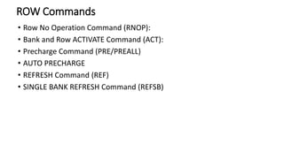
HBM(High Bandwidth
Memory)
-Harinath reddy
Contents
Introduction
HBM2 and HBM2E
HBM Features
Global and each Channel signals
HBM Operating Modes
HBM Channel Addressing
Mode Register set
Write and Read Operation
ROW Commands
COLUMN Commands
References
Introduction
• HBM stands for high bandwidth memory and is a type of memory interface
used in 3D-stacked DRAM (dynamic random access memory) in GPUs, as
well as the server, machine-learning DSP , high-performance computing
and networking and client space.
• HBM uses less power and posts higher bandwidth than on DDR4 or
GDDR5 memory with smaller chips.
• HBM technology works by vertically stacking memory chips on top of one
another. The memory chips are connected through through-silicon vias
(TSVs) and microbumps.
• High bandwidths are essential for the complex AI/ML algorithms needed to
rapidly execute massive calculations and safely implement real-time
decisions on the road.
HBM2 and HBM2E
• HBM memory stack consists of five chips four storage dies above a single logic
die that controls them and speed upto 128 GBps.
• HBM2 debuted in 2016, and in December 2018 the JEDEC updated the HBM2
standard.
• The HBM2 standard called for up to 8 dies in a stack (as with HBM) with an
overall bandwidth of 256 GBps.
• The HBM2E standard allows up to 12 dies per stack for a max capacity of 24GB.
The standard also pegs memory bandwidth at 307 GBps, delivered across a
1,024-bit memory interface separated by 8 unique channels on each stack.
• Outstanding bandwidth, capacity and latency in a powerefficient, compact footprint
make HBM2E memory a superior choice for AI training hardware.
• According to an Ars Technica report, HBM3 is expected to support up to 64GB
capacities and speeds up to 512 GBps.
HBM Features
• 2n prefetch architecture with 256 bits per memory read and write access
• BL = 2 and 4 · 128 DQ width + Optional ECC pin support/channel
• Legacy Mode and Pseudo Channel Mode Operation; (64 DQ width for Pseudo
Channel Mode)
• Differential clock inputs (CK_t/CK_c)
• DDR commands entered on each positive CK_t, CK_c edge. Row Activate
commands require two cycles. All other commands are one cycle command.
• Semi-independent Row & Column Command Interfaces allowing
Activates/Precharges to be issued in parallel with Read/Writes.
• Data referenced to strobes RDQS_t/RDQS_c and WDQS_t/WDQS_c. 1 strobe pair
per DWORD.
• Semi-independent Row & Column Command Interfaces allowing
Activates/Precharges to be issued in parallel with Read/Writes.
• Data referenced to strobes RDQS_t/RDQS_c and WDQS_t/WDQS_c. 1 strobe pair per
DWORD. ·
• Up to 8 channels/stack
• 8 or 16 banks per channel; varies by device density/channel
• Bank Grouping supported · 2K or 4K Bytes per page; varies by device density/channel
• DBIac support configurable via MRS
• Data mask for masking WRITE data per byte
• Self Refresh Modes · I/O voltage 1.2 V
• DRAM core voltage 1.2 V, independent of I/O voltage
• Channel density of 1 Gb to 32 Gb
• Unterminated data/address/cmd/clk interfaces
• Temperature sensor with 3-bit encoded range output
• Each channel provides access to an independent set of DRAM banks.
• Channels are independently clocked, and need not be synchronous.
• Each channel consists of an independent command and data
interface. RESET, IEEE1500 test port and power supply signals are
common to all channels.
• no channel may access the memory storage for a different channel.
• Each channel interface provides an independent interface to a
number of banks of DRAM of a defined Page size.
Single Channel Signal Count & global signal count
HBM operating Modes
• HBM DRAM defines two mode of operation depending on channel
density. 1)Legacy Mode and 2)Pseudo Channel Mode
• Legacy mode provides 256 bit prefetch per memory Read and Write
access. Address bit BA4 is a “Don’t Care” in this mode.
• Pseudo Channel mode divides a channel into two individual sub-channels
of 64 bit I/O each, providing 128 bit prefetch per memory Read and
Write access for each Pseudo channel.
• Both Pseudo channels operate semi independent.
• Both Pseudo channels also share the channel’s mode registers. All I/O
signals of DWORD0 and DWORD1 are associated with Pseudo channel 0,
and all I/O signals of DWORD2 and DWORD3 with Pseudo channel 1.
Pseudo Channel Mode Operation
HBM Channel Addressing
Mode Registers
• The bank group feature is configurable via MRS(Mode Registers set).
• All mode registers are programmed via the Mode Register Set (MRS)
command and retain the stored information until they are
reprogrammed, chip reset, or until the device loses power.
• Mode registers must be loaded when all banks are idle and no bursts are
in progress;
Mode Registers
Operation
• Clocking overview:
• The HBM device captures data on row bus and column bus using differential
CK_t/CK_c.
• The HBM device has uni-directional differential Write strobes (WDQS_t/WDQS_c)
and Read strobes (RDQS_t/RDQS_c) per 32 DQ bits (DWORD).
• HBM Write Data Mask (DM) and Data Bus Inversion (DBIac) Function:
• HBM device supports Data Mask (DM) function for Write operation and Data Bus
Inversion (DBIac) function for Write and Read operation.
• DBI pin is a bi-directional DDR pin and is sampled along with the DQ signals for
Read and Write operation.
• DM pin is bi-directional DDR pin and is sampled along with DQ signals for Read or
Write operation; however DM is input only and is only used for Write operation.
Write & Read Operation
Write Operation:
• HBM device inverts Write data received on the DQ inputs in case DBI is
sampled HIGH, or leaves the Write data non-inverted in case DBI is
sampled LOW. Note that DM input is not affected by the DBIac function.
Read Operation:
• HBM device counts the number of DQ signals that are transitioning from
previous state. Note that DM output is not affected by the DBIac
function.
• The HBM device inverts Read data and sets DBI HIGH when the number
of transitioning data bits within a byte is greater than 4, or when the
number of transitioning data bits within a byte equals 4 and DBI was
High; otherwise the HBM device does not invert the Read data and sets
DBI LOW.
Cont…
ROW Commands
• Row No Operation Command (RNOP):
• Bank and Row ACTIVATE Command (ACT):
• Precharge Command (PRE/PREALL)
• AUTO PRECHARGE
• REFRESH Command (REF)
• SINGLE BANK REFRESH Command (REFSB)
• Row No Operation Command (RNOP):
• It is used to instruct the HBM device to perform a NOP as row command; this
prevents unwanted row commands from being registered during idle or wait
states.
• Bank and Row ACTIVATE Command (ACT):
• Before a READ or WRITE command can be issued to a bank, a row in that bank
must be opened. This is accomplished via the ACTIVATE command, which selects
both the bank and the row to be activated. Once a row is open, a READ or WRITE
command could be issued to that row.
• Precharge Command (PRE/PREALL):
• The PRECHARGE command is used to deactivate the open row in a particular
bank (PRE) or the open rows in all banks (PREALL). The bank(s) will be in idle state
and available for a subsequent row access a specified time tRP after the
PRECHARGE command is issued.
• AUTO PRECHARGE:
• Auto Precharge is a feature which performs the same individual-bank precharge
function described as Precharge, but without requiring an explicit PRECHARGE
command.
• REFRESH Command (REF):
• The REFRESH command is used during normal operation of the HBM device. The
command is received on the row command inputs R[5:0] and requires a CNOP
command on the column command inputs C[7:0].
• Parity is evaluated with the REFRESH command when the parity calculation is
enabled in the Mode Register.
• SINGLE BANK REFRESH Command (REFSB):
• The SINGLE BANK REFRESH command provides an alternative solution for the
refresh of the HBM device. The command initiates a refresh cycle on a single
bank while accesses to other banks including writes and reads are not affected.
COLUMN Commands
• Column No Operation Command (CNOP)
• Read Command (RD, RDA)
• Write Command (WR, WRA)
• Mode Register Set (MRS)
• Power-Mode Commands (Power-Down (PDE, PDX))
• Self-Refresh (SRE, SRX)
• Column No Operation Command (CNOP):
• It is used to instruct the HBM device to perform a NOP as column command; this
prevents unwanted column commands from being registered during idle or wait states.
• Read Command (RD, RDA):
• A read burst is initiated with a READ command . The bank and column addresses are
provided with the READ command and auto precharge is either enabled or disabled for
that access.
• Parity is evaluated with the READ command when the parity calculation is enabled in the
Mode Register.
• Write Command (WR, WRA):
• A Write burst is initiated with a WRITE command. The bank and column addresses are
provided with the WRITE command and auto precharge is either enabled or disabled for
that access.
• Parity is evaluated with the WRITE command when the parity calculation is enabled in
MR0
• Mode Register Set (MRS):
• The MODE REGISTER SET (MRS) command is used to load the Mode Registers of
the HBM device. The command is received on the column command inputs C[7:0]
and requires a RNOP command on the row command inputs R[5:0].
• Power-Mode Commands:
• Power-Down is entered when CKE is registered LOW along with RNOP and CNOP
commands.
• CKE must not go LOW when read or write operations are in progress.
• CKE can go LOW while any other operations such as row activation, precharge,
auto precharge, or refresh are in progress, but the power-down specification will
not apply until such operations are complete.
• Self-Refresh (SRE, SRX):
• Self-refresh can be used to retain data in the HBM device, even if the rest of the
system is powered down. When in the self-refresh mode.
References
• https://www.cs.utah.edu/thememoryforum/mike.pdf
• https://www.design-reuse.com/articles/41186/design-considerations-for-high-
bandwidth-memory-controller.html
• https://www.rambus.com/interface-ip/ddrn-phys/hbm/
• https://go.rambus.com/packaging-solutions-for-ai-and-hpc
• https://go.rambus.com/hbm2e-gddr6-memory-solutions-for-ai
• https://www.rambus.com/rambus-advances-hbm2e-performance-to-4-0-
gbps-for-ai-ml-training-applications/
• https://www.rambus.com/blogs/hbm2e/
• https://www.tomshardware.com/reviews/glossary-hbm-hbm2-high-
bandwidth-memory-definition,5889.html
• https://www.tomshardware.com/reviews/glossary-hbm-hbm2-high-
bandwidth-memory-definition,5889.html

High Bandwidth Memory(HBM)

  • 1.
  • 2.
    Contents Introduction HBM2 and HBM2E HBMFeatures Global and each Channel signals HBM Operating Modes HBM Channel Addressing Mode Register set Write and Read Operation ROW Commands COLUMN Commands References
  • 3.
    Introduction • HBM standsfor high bandwidth memory and is a type of memory interface used in 3D-stacked DRAM (dynamic random access memory) in GPUs, as well as the server, machine-learning DSP , high-performance computing and networking and client space. • HBM uses less power and posts higher bandwidth than on DDR4 or GDDR5 memory with smaller chips. • HBM technology works by vertically stacking memory chips on top of one another. The memory chips are connected through through-silicon vias (TSVs) and microbumps. • High bandwidths are essential for the complex AI/ML algorithms needed to rapidly execute massive calculations and safely implement real-time decisions on the road.
  • 5.
    HBM2 and HBM2E •HBM memory stack consists of five chips four storage dies above a single logic die that controls them and speed upto 128 GBps. • HBM2 debuted in 2016, and in December 2018 the JEDEC updated the HBM2 standard. • The HBM2 standard called for up to 8 dies in a stack (as with HBM) with an overall bandwidth of 256 GBps. • The HBM2E standard allows up to 12 dies per stack for a max capacity of 24GB. The standard also pegs memory bandwidth at 307 GBps, delivered across a 1,024-bit memory interface separated by 8 unique channels on each stack. • Outstanding bandwidth, capacity and latency in a powerefficient, compact footprint make HBM2E memory a superior choice for AI training hardware. • According to an Ars Technica report, HBM3 is expected to support up to 64GB capacities and speeds up to 512 GBps.
  • 6.
    HBM Features • 2nprefetch architecture with 256 bits per memory read and write access • BL = 2 and 4 · 128 DQ width + Optional ECC pin support/channel • Legacy Mode and Pseudo Channel Mode Operation; (64 DQ width for Pseudo Channel Mode) • Differential clock inputs (CK_t/CK_c) • DDR commands entered on each positive CK_t, CK_c edge. Row Activate commands require two cycles. All other commands are one cycle command. • Semi-independent Row & Column Command Interfaces allowing Activates/Precharges to be issued in parallel with Read/Writes. • Data referenced to strobes RDQS_t/RDQS_c and WDQS_t/WDQS_c. 1 strobe pair per DWORD. • Semi-independent Row & Column Command Interfaces allowing Activates/Precharges to be issued in parallel with Read/Writes.
  • 7.
    • Data referencedto strobes RDQS_t/RDQS_c and WDQS_t/WDQS_c. 1 strobe pair per DWORD. · • Up to 8 channels/stack • 8 or 16 banks per channel; varies by device density/channel • Bank Grouping supported · 2K or 4K Bytes per page; varies by device density/channel • DBIac support configurable via MRS • Data mask for masking WRITE data per byte • Self Refresh Modes · I/O voltage 1.2 V • DRAM core voltage 1.2 V, independent of I/O voltage • Channel density of 1 Gb to 32 Gb • Unterminated data/address/cmd/clk interfaces • Temperature sensor with 3-bit encoded range output
  • 8.
    • Each channelprovides access to an independent set of DRAM banks. • Channels are independently clocked, and need not be synchronous. • Each channel consists of an independent command and data interface. RESET, IEEE1500 test port and power supply signals are common to all channels. • no channel may access the memory storage for a different channel. • Each channel interface provides an independent interface to a number of banks of DRAM of a defined Page size.
  • 9.
    Single Channel SignalCount & global signal count
  • 10.
    HBM operating Modes •HBM DRAM defines two mode of operation depending on channel density. 1)Legacy Mode and 2)Pseudo Channel Mode • Legacy mode provides 256 bit prefetch per memory Read and Write access. Address bit BA4 is a “Don’t Care” in this mode. • Pseudo Channel mode divides a channel into two individual sub-channels of 64 bit I/O each, providing 128 bit prefetch per memory Read and Write access for each Pseudo channel. • Both Pseudo channels operate semi independent. • Both Pseudo channels also share the channel’s mode registers. All I/O signals of DWORD0 and DWORD1 are associated with Pseudo channel 0, and all I/O signals of DWORD2 and DWORD3 with Pseudo channel 1.
  • 11.
  • 12.
  • 13.
    Mode Registers • Thebank group feature is configurable via MRS(Mode Registers set). • All mode registers are programmed via the Mode Register Set (MRS) command and retain the stored information until they are reprogrammed, chip reset, or until the device loses power. • Mode registers must be loaded when all banks are idle and no bursts are in progress;
  • 14.
  • 15.
    Operation • Clocking overview: •The HBM device captures data on row bus and column bus using differential CK_t/CK_c. • The HBM device has uni-directional differential Write strobes (WDQS_t/WDQS_c) and Read strobes (RDQS_t/RDQS_c) per 32 DQ bits (DWORD). • HBM Write Data Mask (DM) and Data Bus Inversion (DBIac) Function: • HBM device supports Data Mask (DM) function for Write operation and Data Bus Inversion (DBIac) function for Write and Read operation. • DBI pin is a bi-directional DDR pin and is sampled along with the DQ signals for Read and Write operation. • DM pin is bi-directional DDR pin and is sampled along with DQ signals for Read or Write operation; however DM is input only and is only used for Write operation.
  • 16.
    Write & ReadOperation Write Operation: • HBM device inverts Write data received on the DQ inputs in case DBI is sampled HIGH, or leaves the Write data non-inverted in case DBI is sampled LOW. Note that DM input is not affected by the DBIac function. Read Operation: • HBM device counts the number of DQ signals that are transitioning from previous state. Note that DM output is not affected by the DBIac function. • The HBM device inverts Read data and sets DBI HIGH when the number of transitioning data bits within a byte is greater than 4, or when the number of transitioning data bits within a byte equals 4 and DBI was High; otherwise the HBM device does not invert the Read data and sets DBI LOW.
  • 17.
  • 19.
    ROW Commands • RowNo Operation Command (RNOP): • Bank and Row ACTIVATE Command (ACT): • Precharge Command (PRE/PREALL) • AUTO PRECHARGE • REFRESH Command (REF) • SINGLE BANK REFRESH Command (REFSB)
  • 20.
    • Row NoOperation Command (RNOP): • It is used to instruct the HBM device to perform a NOP as row command; this prevents unwanted row commands from being registered during idle or wait states. • Bank and Row ACTIVATE Command (ACT): • Before a READ or WRITE command can be issued to a bank, a row in that bank must be opened. This is accomplished via the ACTIVATE command, which selects both the bank and the row to be activated. Once a row is open, a READ or WRITE command could be issued to that row. • Precharge Command (PRE/PREALL): • The PRECHARGE command is used to deactivate the open row in a particular bank (PRE) or the open rows in all banks (PREALL). The bank(s) will be in idle state and available for a subsequent row access a specified time tRP after the PRECHARGE command is issued.
  • 21.
    • AUTO PRECHARGE: •Auto Precharge is a feature which performs the same individual-bank precharge function described as Precharge, but without requiring an explicit PRECHARGE command. • REFRESH Command (REF): • The REFRESH command is used during normal operation of the HBM device. The command is received on the row command inputs R[5:0] and requires a CNOP command on the column command inputs C[7:0]. • Parity is evaluated with the REFRESH command when the parity calculation is enabled in the Mode Register. • SINGLE BANK REFRESH Command (REFSB): • The SINGLE BANK REFRESH command provides an alternative solution for the refresh of the HBM device. The command initiates a refresh cycle on a single bank while accesses to other banks including writes and reads are not affected.
  • 22.
    COLUMN Commands • ColumnNo Operation Command (CNOP) • Read Command (RD, RDA) • Write Command (WR, WRA) • Mode Register Set (MRS) • Power-Mode Commands (Power-Down (PDE, PDX)) • Self-Refresh (SRE, SRX)
  • 23.
    • Column NoOperation Command (CNOP): • It is used to instruct the HBM device to perform a NOP as column command; this prevents unwanted column commands from being registered during idle or wait states. • Read Command (RD, RDA): • A read burst is initiated with a READ command . The bank and column addresses are provided with the READ command and auto precharge is either enabled or disabled for that access. • Parity is evaluated with the READ command when the parity calculation is enabled in the Mode Register. • Write Command (WR, WRA): • A Write burst is initiated with a WRITE command. The bank and column addresses are provided with the WRITE command and auto precharge is either enabled or disabled for that access. • Parity is evaluated with the WRITE command when the parity calculation is enabled in MR0
  • 24.
    • Mode RegisterSet (MRS): • The MODE REGISTER SET (MRS) command is used to load the Mode Registers of the HBM device. The command is received on the column command inputs C[7:0] and requires a RNOP command on the row command inputs R[5:0]. • Power-Mode Commands: • Power-Down is entered when CKE is registered LOW along with RNOP and CNOP commands. • CKE must not go LOW when read or write operations are in progress. • CKE can go LOW while any other operations such as row activation, precharge, auto precharge, or refresh are in progress, but the power-down specification will not apply until such operations are complete. • Self-Refresh (SRE, SRX): • Self-refresh can be used to retain data in the HBM device, even if the rest of the system is powered down. When in the self-refresh mode.
  • 25.
    References • https://www.cs.utah.edu/thememoryforum/mike.pdf • https://www.design-reuse.com/articles/41186/design-considerations-for-high- bandwidth-memory-controller.html •https://www.rambus.com/interface-ip/ddrn-phys/hbm/ • https://go.rambus.com/packaging-solutions-for-ai-and-hpc • https://go.rambus.com/hbm2e-gddr6-memory-solutions-for-ai • https://www.rambus.com/rambus-advances-hbm2e-performance-to-4-0- gbps-for-ai-ml-training-applications/ • https://www.rambus.com/blogs/hbm2e/ • https://www.tomshardware.com/reviews/glossary-hbm-hbm2-high- bandwidth-memory-definition,5889.html • https://www.tomshardware.com/reviews/glossary-hbm-hbm2-high- bandwidth-memory-definition,5889.html