Download as PDF, PPTX
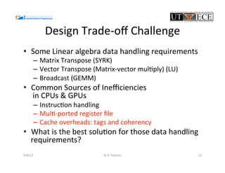

![Data
Handling
Trade-‐off
in
Core
• GEMM[ASAP2011]
– Regular
data
movement
– Regular
access
paoern
– Easily
mapped
on
most
SIMD
Cores
• SYRK[ASAP2012],[SBAC-‐PAD2012]
– Matrix
Transpose
needed
– Data
manipula#on
for
Transpose
is
a
challenge
9/8/13
12
©
A.
Pedram](https://image.slidesharecdn.com/ardavanblisretreat2013-180329213403/85/Custom-Computer-Engine-for-Optimizing-for-the-Inner-kernel-of-Matrix-Multiplication-12-320.jpg)
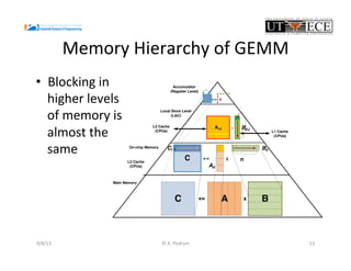

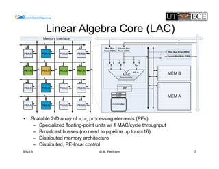
![Power
and
Performance
Analysis
• Analy#cal
formulae
– U#liza#on
– Bandwidth
– Size
of
local
stores
– Size
of
register
file
– #ports
of
memory
levels
• Component
selec#ons
– Storage
model
[CACTI
6.5]
• Pure
SRAM
Model
for
Register
file
• Cache
Models
for
L1
&
L2
• Configura#on
– 1
GHz
– 16
FPUs
– LAC
• 256+32
KB
aggregate
Local
store
– Register
file
organiza#ons
• 256
KB
L2,
64B
line,
8
way
• 32
KB
L1,
64B
line,
8way
• Register
file
Size
variable
– Aimed
for
peak
performance
9/8/13
17
©
A.
Pedram](https://image.slidesharecdn.com/ardavanblisretreat2013-180329213403/85/Custom-Computer-Engine-for-Optimizing-for-the-Inner-kernel-of-Matrix-Multiplication-17-320.jpg)

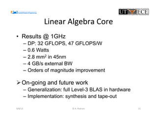


The document presents the design and performance optimization of a low-power, high-performance linear algebra core (LAC) tailored for matrix multiplication kernels, specifically focusing on the General Matrix Multiply (GEMM). It discusses the challenges posed by traditional architectures in handling linear algebra operations and proposes a specialized structure that leverages SIMD (Single Instruction, Multiple Data) capabilities and efficient data handling mechanisms. Finally, it provides performance metrics and emphasizes the potential for future enhancements, including the implementation of broader BLAS functionalities in hardware.