Download as PDF, PPTX


![Ahmed Ennaoui / Helmholtz-Zentrum Berlin für Materialien und Energie
Introduction: Key Task of Photovoltaic
Power [Watt/cm2] = Voltage [Volt ] x Current density [A/cm2]
PV products can be optimized for
location, with lower associated financial
risk based on predictable performance
Key aim is to generate electricity from solar spectrum
EFFECIENCY INCREASING
LESS AREA
LESS MATERIAL
COST FOR PV REDUCED
LOW €/Wp
Materials with small Band gap
But low voltage
Excess energy lost to heat
Generating a large current (JSC)
Materials with large band gap
But low current
Sub-band gap light is lost
Generating a large voltage (VOC)
Two challenges
Solar cell design
versus
solar spectrum
Voltage [Volt ]
JSC[A/cm2]
Power[Watt/cm2]
VOC
0
JSC
maximum
power
point
Jm
Vm
Vm x Jm
AM1,5](https://image.slidesharecdn.com/rdroadmapennaoui-130906055530-/75/Thin-Film-Photovoltaics-R-D-Innovation-Opportunities_Ennaoui-7-2048.jpg)
![Efficiencies beyond the Shockley-Queisser limit
500 1000 1500 2000 2500
0
200
400
600
800
1000
1200
1400
1600
Leistungsdichte[W/m
2
µm]
AM15
GaInP
GaInAs
Ge
Wellenlänge [nm]
(1) Lattice thermalization loss (> 50%)
(2) Transparency to h < Band gap
(3) Recombination Loss
(4) Current flow
(5) Contact voltage loss
Not all the energy of absorbed photon
can be captured for productive use.
(Th. Maxi efficiency ~32% ).
source
1.7 eV
1.1 eV
0.7 eV
R.R. King; Spectrolab Inc., AVS 54th International Symposium, Seattle 2007
Optimistic calculation
Best commercially available cells 37% efficient at 25°C.
75% efficient 0.30 × 0.75 × 850 ≈ 200 W/m2 of electrical power.
At $200/m2 the capital cost would be $1.50/W.](https://image.slidesharecdn.com/rdroadmapennaoui-130906055530-/75/Thin-Film-Photovoltaics-R-D-Innovation-Opportunities_Ennaoui-8-2048.jpg)


![Design to high efficiency solar cells
Light trapping
Reflection Loss: ARC
Material
Parameter
absorption
Important cost factor
thikness
€
αW
p
e
αL1
1
1R)(1η
λ
hc
e
)J(
Φ(λ)
1
N
N
η photons
in
electron
out
Decisive Material
Parameter
The band gap
0.3 0.5 0.7 0.9 1.1
20
0
40
60
80
100
0
1
2
3
4
5
NumberofSunlightPhotons(m-2s-1micron-1)E+19
RExternalQuantumEfficiency,%
c-Si:H junctiona-Si:H junction
AM 1.5 global spectrum
Wavelength, microns
a-Si:H/c-Si:H Cell Spectral Response
Textured TCO
a-Si
Top cell
Back
Reflector
Glass
substrate
Thin film mc-
Si
Bottom cell
GE
λ0λsc dλ.dα-exp.)().ΦR(1.η(λ).qJ
Light from the sun
C10x1.6e
][A.mCurrent
N 19
-2
electron
out
energy[J]photon
][J.mEnergyInput
N
-2
Photon
in ](https://image.slidesharecdn.com/rdroadmapennaoui-130906055530-/75/Thin-Film-Photovoltaics-R-D-Innovation-Opportunities_Ennaoui-19-2048.jpg)


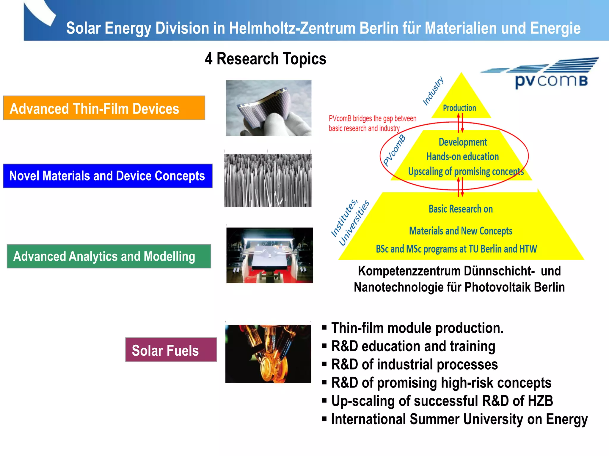
This document discusses thin-film photovoltaics research and opportunities. It covers several topics: - Thin-film solar cell technologies like CIGS, CdTe, and emerging materials like CZTS have higher efficiencies than earlier generations and lower production costs. Research aims to further improve efficiency and reduce costs. - The Helmholtz-Zentrum in Berlin conducts R&D on thin-film photovoltaics including advanced materials, device concepts, and characterization techniques to develop more efficient and cost-effective solar cells. - Issues like material scarcity for some thin-film technologies are being addressed through research into alternative materials and processes to produce solar cells on flexible substrates using less raw


![Coded Agents – with UiPath SDK + LangGraph [Virtual Hands-on Workshop]](https://cdn.slidesharecdn.com/ss_thumbnails/codedagentsdeck-251215155422-5497c599-thumbnail.jpg?width=640&height=640&fit=bounds)


