SlideShare a Scribd company logo
Department of Electrical and
Computer Engineering
ECSE-330B Electronic Circuits I
MOSFETs 1
Biasing in MOSFET Amplifiers
• Biasing: Creating the circuit to establish the desired
DC voltages and currents for the operation of the
amplifier
• Four common ways:
1. Biasing by fixing VGS
2. Biasing by fixing VG and connecting a resistance in the
Source
3. Biasing using a Drain-to-Gate Feedback Resistor
4. Biasing Using a Constant-Current Source
Department of Electrical and
Computer Engineering
ECSE-330B Electronic Circuits I
MOSFETs 2
Biasing in MOSFET Amplifiers
• Biasing by fixing VGS
When the MOSFET device is
changed (even using the same
supplier), this method can result in
a large variability in the value of
ID. Devices 1 and 2 represent
extremes among units of the same
type.
( )2
2
1
t
GS
n
D V
V
L
W
k
I −
′
=
ox
n
ox
ox
n
n C
t
k μ
ε
μ =
=
′
VDD
-VEE
VGG
RG
RD
RS
M1
VG
VD
VS
Department of Electrical and
Computer Engineering
ECSE-330B Electronic Circuits I
MOSFETs 3
Biasing in MOSFET Amplifiers
• Biasing by fixing VG and connecting a resistance in the Source
Degeneration Resistance
Department of Electrical and
Computer Engineering
ECSE-330B Electronic Circuits I
MOSFETs 4
Biasing in MOSFET Amplifiers
• Biasing using a Drain-to-Gate Feedback Resistor
Large Resistor
Department of Electrical and
Computer Engineering
ECSE-330B Electronic Circuits I
MOSFETs 5
Biasing in MOSFET Amplifiers
• Biasing Using a Constant-Current Source
Figure 4.33 (a) Biasing the MOSFET using a constant-current source I. (b) Implementation of the constant-current source I
using a current mirror.
Current Mirror
Used in Integrated Circuits
Department of Electrical and
Computer Engineering
ECSE-330B Electronic Circuits I
MOSFETs 6
Current Mirror DC Analysis
• The width and length (the W/L aspect
ratio) and the parameters of the two
transistors can be different
• We can choose W/L freely
• In this circuit, consider W/L of both
MOSFETs are the same and transistors
are identical. The Gate-Source voltages
are also the same, then
( )2
1
1
2
1
t
GS
n
REF V
V
L
W
k
I −
′
=
( )2
1
1
2
1
t
GS
n V
V
L
W
k
I −
′
=
REF
REF
I
I
W
L
L
W
I
I
=
=
⋅
= 1
1
1
1
1
W1
L1
VGS VGS
+
-
-
+
W1
L1
I
Department of Electrical and
Computer Engineering
ECSE-330B Electronic Circuits I
MOSFETs 7
Current Mirror DC Analysis
• Designing IREF
R
V
V
V
I SS
GS
DD
REF
+
−
=
( )2
1
1
2
1
t
GS
n
REF V
V
L
W
k
I −
′
=
• It is often needed to find the value of R in order to
achieve a desired IREF
Department of Electrical and
Computer Engineering
ECSE-330B Electronic Circuits I
MOSFETs 8
Biasing of MOSFET Amplifier
• 1- Intro to MOS Field Effect Transistor (MOSFET)
• 2- NMOS FET
• 3- PMOS FET
• 4- DC Analysis of MOSFET Circuits
• 5- MOSFET Amplifier
• 6- MOSFET Small Signal Model
• 7- MOSFET Integrated Circuits
• 8- CSA, CGA, CDA
• 9- CMOS Inverter & MOS Digital Logic
Department of Electrical and
Computer Engineering
ECSE-330B Electronic Circuits I
MOSFETs 9
MOSFET Design Space
• Modern integrated circuits use MOSFETs
extensively
– Very high densities of transistors – up to 109
transistors/cm2 in some ULSI memory arrays.
– Off-chip discrete resistors and capacitors are NOT
commonly used
– On-chip resistors and capacitors generally small
– Multistage amplifiers are usually DC-coupled
• Transistors used wherever possible to implement
current sources, resistors, capacitors,
Department of Electrical and
Computer Engineering
ECSE-330B Electronic Circuits I
MOSFETs 10
Using MOSFETs to implement R’s and C’s
• Resistors:
Active Loads (large R’s)
Diode-connected loads (small R’s)
MOSFET Triode-Region (moderate R’s)
• Capacitors
Most obvious is the gate-body capacitor
Can be used to have variable-capacitors as well
• Current Mirrors
Department of Electrical and
Computer Engineering
ECSE-330B Electronic Circuits I
MOSFETs 11
MOSFET Active Loads
• MOSFETs used as an active load for high resistances:
– MOSFET is held in saturation with the source and gate
held at a constant DC voltage
– Drain connected to circuit
vgs = 0
gmvgs = 0
D
o
I
r
⋅
=
λ
1
– ro is inversely proportional to ID
Rin= ?
Rin=ro
Department of Electrical and
Computer Engineering
ECSE-330B Electronic Circuits I
MOSFETs 12
Diode-Connected MOSFETs
• A Diode connected MOSFET can be used to achieve
small resistances:
– The Drain is directly connected to Gate, and therefore it
can only be operated in saturation (or cutoff)
Source Absorption Theorem
Department of Electrical and
Computer Engineering
ECSE-330B Electronic Circuits I
MOSFETs 13
MOSFET Current Mirrors
• Used extensively in
MOSFET IC applications
• Often ro,is neglected. Since
there is no gate current, the
drain currents of M1 and M2
are identical
• In practice, IREF ≠ I due to
finite ro. (Not included in EC1)
VGS VGS
+
-
-
+
0 0
( ) )
1
(
2
1 2
1
1
X
t
X
n
REF V
V
V
L
W
k
I λ
+
−
′
=
1
1 DS
GS
X V
V
V =
=
VX
The current I will also depend on VDS2
I
Department of Electrical and
Computer Engineering
ECSE-330B Electronic Circuits I
MOSFETs 14
Current Mirror DC Analysis
• The width and length (the W/L
aspect ratio) of MOSFETs can
be designed almost freely
• Since the W/L of M1 and M2
need not be the same, the size
ratios can affect current ratios
( )2
1
1
2
1
t
GS
n
REF V
V
L
W
k
I −
′
=
( )2
2
2
2
1
t
GS
n V
V
L
W
k
I −
′
=
1
1
2
2
W
L
L
W
I
I
REF
⋅
=
W1
L1
W2
L2
VGS VGS
+
-
-
+
I
Department of Electrical and
Computer Engineering
ECSE-330B Electronic Circuits I
MOSFETs 15
Current Scaling (Steering)
• Ratio of
aspect ratios
can be
selected to
achieve
nearly any
scale factor
I/IREF
W
L
W
L
W
L
W
L
Note: All gates are connected
Department of Electrical and
Computer Engineering
ECSE-330B Electronic Circuits I
MOSFETs 16
Current Mirroring – Pushing and Pulling
Department of Electrical and
Computer Engineering
ECSE-330B Electronic Circuits I
MOSFETs 17
Small Signal
• Transistor M1 is diode
connected and acts like a
resistor to s.-s. ground.
ro2
Department of Electrical and
Computer Engineering
ECSE-330B Electronic Circuits I
MOSFETs 18
Outline of Chapter 5
• 1- Intro to MOS Field Effect Transistor (MOSFET)
• 2- NMOS FET
• 3- PMOS FET
• 4- DC Analysis of MOSFET Circuits
• 5- MOSFET Amplifier
• 6- MOSFET Small Signal Model
• 7- MOSFET Integrated Circuits
• 8- CSA, CGA, CDA
• 9- CMOS Inverter & MOS Digital Logic
Department of Electrical and
Computer Engineering
ECSE-330B Electronic Circuits I
MOSFETs 19
DC and AC - Body-Effect / CLM
Three types of analysis:
Neglect AC Body-Effect & AC CLM
/ Neglect AC CLM
Use AC Body-Effect
Use AC Body-Effect / Use CLM
Three types of analysis:
Neglect DC Body-Effect & DC CLM
/ Neglect DC CLM
Use DC Body-Effect
Use DC Body-Effect / Use DC CLM
DC Analysis
AC Analysis
(small-signal)
Use whatever
DC values for
V and I in the
small-signal
analysis
Department of Electrical and
Computer Engineering
ECSE-330B Electronic Circuits I
MOSFETs 20
Common Source Amplifier (CSA)
• Current source I implemented
with current mirror.
• Current mirror provides
active load at drain
• Source terminal grounded –
no DC or AC Body effect
Department of Electrical and
Computer Engineering
ECSE-330B Electronic Circuits I
MOSFETs 21
CSA with Current Mirror
CSA
ro2
Department of Electrical and
Computer Engineering
ECSE-330B Electronic Circuits I
MOSFETs 22
CSA Small Signal Analysis
• From MOSFET
Current-Mirror:
only ro2 appears in
analysis
i
gs v
v =
1
( ) 1
2
1
1 gs
o
o
m
out v
r
r
g
v −
=
( )
2
1
1 o
o
m
i
out
V r
r
g
v
v
A −
=
=
Department of Electrical and
Computer Engineering
ECSE-330B Electronic Circuits I
MOSFETs 23
CSA Input/Output Resistance
• Input Resistance
• Output resistance
2
1 o
o
OUT r
r
R =
vgs1 = 0
gm1vgs1 = 0
∞
⇒
IN
R
Department of Electrical and
Computer Engineering
ECSE-330B Electronic Circuits I
MOSFETs 24
CSA Calculations
• In practice, difficult to keep all
transistors operating in saturation
VOUT is hard to control, and
sensitive to: W/L, VG, and
CLM
Ω
=
−
=
=
=
=
=
′
=
′
=
=
=
= −
k
R
V
V
V
V
L
W
L
W
k
k
V
V
V
V
REF
SS
DD
V
A
n
V
A
p
t
t
1
2
,
5
40
,
50
125
50
1
01
.
0
1
1
2
2
2
1
1
2
1
μ
μ
λ
λ
V
V
V
o
V
A
m
OUT
G
A
k
r
m
g
V
V
mA
I
V
V
100
52
.
38
192
.
5
855
.
3
596
.
2
567
.
2
1
−
=
Ω
=
=
=
=
=
Hand: SPICE:
V
V
V
OUT
G
A
V
V
mA
I
V
V
4
.
102
895
.
2
57
.
2
58
.
2
−
=
=
=
=
Department of Electrical and
Computer Engineering
ECSE-330B Electronic Circuits I
MOSFETs 25
Common Gate Amplifier (CGA)
• A pMOS current mirror is used
as IREF including the output
resistance.
• Since source terminal not at
signal ground, the body effect is
present.
• The gate terminal held at a DC
voltage. (AC Ground)
Typically used as second stage of a
multi-stage amplifier circuit
Department of Electrical and
Computer Engineering
ECSE-330B Electronic Circuits I
MOSFETs 26
CGA – DC Analysis
• Current mirror is assumed to be ideal
during the DC analysis, thus IREF=I
• DC voltage at the source terminal (VS)
must be obtained from driving the
current IREF through the transistor.
• This assumes that the input voltage
source VI is set to zero
• RI is part of the source voltage
• Solve for VO, with VS and VG known,
and including CLM
( ) ( )
[ ]
S
O
t
S
G
n V
V
V
V
V
L
W
k
I −
⋅
+
−
−
′
= λ
1
2
2
1
Department of Electrical and
Computer Engineering
ECSE-330B Electronic Circuits I
MOSFETs 27
CGA
• Replace with a current source
including output resistance ro2
Choice of analysis:
Neglect AC Body-Effect & CLM
/ Neglect CLM
Use AC Body-Effect
Use AC Body-Effect / Use CLM
ro2
Department of Electrical and
Computer Engineering
ECSE-330B Electronic Circuits I
MOSFETs 28
CGA – No Body Effect or CLM
2
o
gs
m
o r
v
g
v ⋅
−
=
I
I
m
m
gs v
R
g
g
v
+
−
=
1
1
1
1
I
m
o
I
o
V
R
g
r
v
v
A
+
=
=
1
2
i=0
Non Inverting
Department of Electrical and
Computer Engineering
ECSE-330B Electronic Circuits I
MOSFETs 29
CGA – RIN & ROUT, No Body Effect or CLM
1
1
m
IN
g
R =
RIN
ROUT
2
o
OUT r
R =
vI = 0
Department of Electrical and
Computer Engineering
ECSE-330B Electronic Circuits I
MOSFETs 30
CGA – With Body Effect & no CLM
( ) 2
1
1 o
x
mb
x
m
o r
v
g
v
g
v +
−
=
( ) 2
1
1 o
mb
m
x
o
V r
g
g
v
v
A +
=
=
x
gs
bs v
v
v −
=
= 1
1
( ) 2
1
1
1
1 o
bs
mb
gs
m
o r
v
g
v
g
v +
−
=
( )
I
IN
IN
o
mb
m
i
x
x
o
i
o
total
V
R
R
R
r
g
g
v
v
v
v
v
v
A
+
⋅
+
=
⋅
=
=
− 2
Include RI and
solve for total
voltage gain in
term of RIN
RIN
Solve at vx first:
vX
Department of Electrical and
Computer Engineering
ECSE-330B Electronic Circuits I
MOSFETs 31
CGA – RIN With Body Effect & no CLM
x
mb
m
x v
g
g
i )
( 1
1 +
=
x
gs
bs v
v
v −
=
= 1
1
1
1
1
mb
m
IN
g
g
R
+
=
RIN
iIN
vX
Neglect Input
Voltage Source
x
mb
m
in v
g
g
i )
( 1
1 +
=
iX
Department of Electrical and
Computer Engineering
ECSE-330B Electronic Circuits I
MOSFETs 32
CGA - With Body Effect & CLM
Neglect Input
Voltage Source
gs
x v
v −
=
2
o
x
o r
i
v ⋅
=
( )
1
1
1
o
o
x
x
mb
m
x
r
v
v
v
g
g
i
−
+
+
=
vX
iX
iX
( ) ⎟
⎟
⎠
⎞
⎜
⎜
⎝
⎛
+
+
⋅
=
= 1
1
1
2
1
1
mb
m
o
o
o
x
o
V g
g
r
r
r
v
v
A
Department of Electrical and
Computer Engineering
ECSE-330B Electronic Circuits I
MOSFETs 33
CGA – RIN With Body Effect & CLM
Neglect Input
Voltage Source
2
o
x
o r
i
v ⋅
=
( )
1
1
1
o
o
x
x
mb
m
x
r
v
v
v
g
g
i
−
+
+
=
1
1
1
1
2
1
1
mb
m
o
o
o
x
x
IN
g
g
r
r
r
i
v
R
+
+
+
=
=
RIN
iX
vX

More Related Content

Similar to 4.4 MOSFETS in IC CSA CGA.pdf

Iii eie ii sem pe lab manual(ee382)
Iii eie ii sem pe lab manual(ee382)Iii eie ii sem pe lab manual(ee382)
Iii eie ii sem pe lab manual(ee382)
Karthik Prof.
 
Ped lab 2017 reg manual
Ped lab 2017 reg manualPed lab 2017 reg manual
Differentiator.ppt
Differentiator.pptDifferentiator.ppt
Differentiator.ppt
PonnalaguRN1
 
pe lab manual
pe lab manualpe lab manual
pe lab manual
saisureshnaidu
 
Electronic DC Voltmeter using PMMC
Electronic DC Voltmeter using PMMCElectronic DC Voltmeter using PMMC
Electronic DC Voltmeter using PMMC
Dr Naim R Kidwai
 
4. single stage amplifier
4. single stage amplifier4. single stage amplifier
4. single stage amplifier
ShahbazQamar2
 
Bjt amplifiers
Bjt amplifiersBjt amplifiers
Bjt amplifiers
Gastarot
 
Regions of operation of bjt and mosfet
Regions of operation of bjt and mosfetRegions of operation of bjt and mosfet
Regions of operation of bjt and mosfet
MahoneyKadir
 
Automatic Night Light/ Street Light
Automatic Night Light/ Street LightAutomatic Night Light/ Street Light
Automatic Night Light/ Street Light
Sankarshan D
 
CMOS Analog IC design by Dr GS Javed - Refresher Course - Batch 1
CMOS Analog IC design by Dr GS Javed - Refresher Course - Batch 1CMOS Analog IC design by Dr GS Javed - Refresher Course - Batch 1
CMOS Analog IC design by Dr GS Javed - Refresher Course - Batch 1
Javed G S, PhD
 
5 transistor applications
5 transistor applications5 transistor applications
5 transistor applications
dataniyaarunkumar
 
Lect2 up380 (100329)
Lect2 up380 (100329)Lect2 up380 (100329)
Lect2 up380 (100329)aicdesign
 
Ac analysis of bjt and mosfet inverting amplifiers
Ac analysis of bjt and mosfet inverting amplifiersAc analysis of bjt and mosfet inverting amplifiers
Ac analysis of bjt and mosfet inverting amplifiers
MahoneyKadir
 
Ac analysis of bjt and mosfet inverting amplifiers
Ac analysis of bjt and mosfet inverting amplifiersAc analysis of bjt and mosfet inverting amplifiers
Ac analysis of bjt and mosfet inverting amplifiers
MahoneyKadir
 
Circuit Analysis Lab
Circuit Analysis LabCircuit Analysis Lab
Circuit Analysis LabSachin Airan
 
Lecture 8
Lecture 8Lecture 8
Lecture 8
Forward2025
 
Transistors - JFET, MOSFET, UJT & 555 Timer
Transistors - JFET, MOSFET, UJT & 555 TimerTransistors - JFET, MOSFET, UJT & 555 Timer
Transistors - JFET, MOSFET, UJT & 555 Timer
Dhivya Ramachandran
 
Ic 555 timer 0
Ic 555 timer 0Ic 555 timer 0
Ic 555 timer 0
chitradevitvm
 

Similar to 4.4 MOSFETS in IC CSA CGA.pdf (20)

Iii eie ii sem pe lab manual(ee382)
Iii eie ii sem pe lab manual(ee382)Iii eie ii sem pe lab manual(ee382)
Iii eie ii sem pe lab manual(ee382)
 
Ped lab 2017 reg manual
Ped lab 2017 reg manualPed lab 2017 reg manual
Ped lab 2017 reg manual
 
Differentiator.ppt
Differentiator.pptDifferentiator.ppt
Differentiator.ppt
 
pe lab manual
pe lab manualpe lab manual
pe lab manual
 
SAIKAT-VECC final
SAIKAT-VECC finalSAIKAT-VECC final
SAIKAT-VECC final
 
ICIECA 2014 Paper 23
ICIECA 2014 Paper 23ICIECA 2014 Paper 23
ICIECA 2014 Paper 23
 
Electronic DC Voltmeter using PMMC
Electronic DC Voltmeter using PMMCElectronic DC Voltmeter using PMMC
Electronic DC Voltmeter using PMMC
 
4. single stage amplifier
4. single stage amplifier4. single stage amplifier
4. single stage amplifier
 
Bjt amplifiers
Bjt amplifiersBjt amplifiers
Bjt amplifiers
 
Regions of operation of bjt and mosfet
Regions of operation of bjt and mosfetRegions of operation of bjt and mosfet
Regions of operation of bjt and mosfet
 
Automatic Night Light/ Street Light
Automatic Night Light/ Street LightAutomatic Night Light/ Street Light
Automatic Night Light/ Street Light
 
CMOS Analog IC design by Dr GS Javed - Refresher Course - Batch 1
CMOS Analog IC design by Dr GS Javed - Refresher Course - Batch 1CMOS Analog IC design by Dr GS Javed - Refresher Course - Batch 1
CMOS Analog IC design by Dr GS Javed - Refresher Course - Batch 1
 
5 transistor applications
5 transistor applications5 transistor applications
5 transistor applications
 
Lect2 up380 (100329)
Lect2 up380 (100329)Lect2 up380 (100329)
Lect2 up380 (100329)
 
Ac analysis of bjt and mosfet inverting amplifiers
Ac analysis of bjt and mosfet inverting amplifiersAc analysis of bjt and mosfet inverting amplifiers
Ac analysis of bjt and mosfet inverting amplifiers
 
Ac analysis of bjt and mosfet inverting amplifiers
Ac analysis of bjt and mosfet inverting amplifiersAc analysis of bjt and mosfet inverting amplifiers
Ac analysis of bjt and mosfet inverting amplifiers
 
Circuit Analysis Lab
Circuit Analysis LabCircuit Analysis Lab
Circuit Analysis Lab
 
Lecture 8
Lecture 8Lecture 8
Lecture 8
 
Transistors - JFET, MOSFET, UJT & 555 Timer
Transistors - JFET, MOSFET, UJT & 555 TimerTransistors - JFET, MOSFET, UJT & 555 Timer
Transistors - JFET, MOSFET, UJT & 555 Timer
 
Ic 555 timer 0
Ic 555 timer 0Ic 555 timer 0
Ic 555 timer 0
 

Recently uploaded

[JPP-1] - (JEE 3.0) - Kinematics 1D - 14th May..pdf
[JPP-1] - (JEE 3.0) - Kinematics 1D - 14th May..pdf[JPP-1] - (JEE 3.0) - Kinematics 1D - 14th May..pdf
[JPP-1] - (JEE 3.0) - Kinematics 1D - 14th May..pdf
awadeshbabu
 
01-GPON Fundamental fttx ftth basic .pptx
01-GPON Fundamental fttx ftth basic .pptx01-GPON Fundamental fttx ftth basic .pptx
01-GPON Fundamental fttx ftth basic .pptx
benykoy2024
 
Unbalanced Three Phase Systems and circuits.pptx
Unbalanced Three Phase Systems and circuits.pptxUnbalanced Three Phase Systems and circuits.pptx
Unbalanced Three Phase Systems and circuits.pptx
ChristineTorrepenida1
 
ACRP 4-09 Risk Assessment Method to Support Modification of Airfield Separat...
ACRP 4-09 Risk Assessment Method to Support Modification of Airfield Separat...ACRP 4-09 Risk Assessment Method to Support Modification of Airfield Separat...
ACRP 4-09 Risk Assessment Method to Support Modification of Airfield Separat...
Mukeshwaran Balu
 
14 Template Contractual Notice - EOT Application
14 Template Contractual Notice - EOT Application14 Template Contractual Notice - EOT Application
14 Template Contractual Notice - EOT Application
SyedAbiiAzazi1
 
一比一原版(SFU毕业证)西蒙菲莎大学毕业证成绩单如何办理
一比一原版(SFU毕业证)西蒙菲莎大学毕业证成绩单如何办理一比一原版(SFU毕业证)西蒙菲莎大学毕业证成绩单如何办理
一比一原版(SFU毕业证)西蒙菲莎大学毕业证成绩单如何办理
bakpo1
 
Hierarchical Digital Twin of a Naval Power System
Hierarchical Digital Twin of a Naval Power SystemHierarchical Digital Twin of a Naval Power System
Hierarchical Digital Twin of a Naval Power System
Kerry Sado
 
Literature Review Basics and Understanding Reference Management.pptx
Literature Review Basics and Understanding Reference Management.pptxLiterature Review Basics and Understanding Reference Management.pptx
Literature Review Basics and Understanding Reference Management.pptx
Dr Ramhari Poudyal
 
一比一原版(IIT毕业证)伊利诺伊理工大学毕业证成绩单专业办理
一比一原版(IIT毕业证)伊利诺伊理工大学毕业证成绩单专业办理一比一原版(IIT毕业证)伊利诺伊理工大学毕业证成绩单专业办理
一比一原版(IIT毕业证)伊利诺伊理工大学毕业证成绩单专业办理
zwunae
 
Nuclear Power Economics and Structuring 2024
Nuclear Power Economics and Structuring 2024Nuclear Power Economics and Structuring 2024
Nuclear Power Economics and Structuring 2024
Massimo Talia
 
sieving analysis and results interpretation
sieving analysis and results interpretationsieving analysis and results interpretation
sieving analysis and results interpretation
ssuser36d3051
 
Series of visio cisco devices Cisco_Icons.ppt
Series of visio cisco devices Cisco_Icons.pptSeries of visio cisco devices Cisco_Icons.ppt
Series of visio cisco devices Cisco_Icons.ppt
PauloRodrigues104553
 
PROJECT FORMAT FOR EVS AMITY UNIVERSITY GWALIOR.ppt
PROJECT FORMAT FOR EVS AMITY UNIVERSITY GWALIOR.pptPROJECT FORMAT FOR EVS AMITY UNIVERSITY GWALIOR.ppt
PROJECT FORMAT FOR EVS AMITY UNIVERSITY GWALIOR.ppt
bhadouriyakaku
 
Swimming pool mechanical components design.pptx
Swimming pool  mechanical components design.pptxSwimming pool  mechanical components design.pptx
Swimming pool mechanical components design.pptx
yokeleetan1
 
bank management system in java and mysql report1.pdf
bank management system in java and mysql report1.pdfbank management system in java and mysql report1.pdf
bank management system in java and mysql report1.pdf
Divyam548318
 
Modelagem de um CSTR com reação endotermica.pdf
Modelagem de um CSTR com reação endotermica.pdfModelagem de um CSTR com reação endotermica.pdf
Modelagem de um CSTR com reação endotermica.pdf
camseq
 
一比一原版(UMich毕业证)密歇根大学|安娜堡分校毕业证成绩单专业办理
一比一原版(UMich毕业证)密歇根大学|安娜堡分校毕业证成绩单专业办理一比一原版(UMich毕业证)密歇根大学|安娜堡分校毕业证成绩单专业办理
一比一原版(UMich毕业证)密歇根大学|安娜堡分校毕业证成绩单专业办理
zwunae
 
一比一原版(Otago毕业证)奥塔哥大学毕业证成绩单如何办理
一比一原版(Otago毕业证)奥塔哥大学毕业证成绩单如何办理一比一原版(Otago毕业证)奥塔哥大学毕业证成绩单如何办理
一比一原版(Otago毕业证)奥塔哥大学毕业证成绩单如何办理
dxobcob
 
KuberTENes Birthday Bash Guadalajara - K8sGPT first impressions
KuberTENes Birthday Bash Guadalajara - K8sGPT first impressionsKuberTENes Birthday Bash Guadalajara - K8sGPT first impressions
KuberTENes Birthday Bash Guadalajara - K8sGPT first impressions
Victor Morales
 
digital fundamental by Thomas L.floydl.pdf
digital fundamental by Thomas L.floydl.pdfdigital fundamental by Thomas L.floydl.pdf
digital fundamental by Thomas L.floydl.pdf
drwaing
 

Recently uploaded (20)

[JPP-1] - (JEE 3.0) - Kinematics 1D - 14th May..pdf
[JPP-1] - (JEE 3.0) - Kinematics 1D - 14th May..pdf[JPP-1] - (JEE 3.0) - Kinematics 1D - 14th May..pdf
[JPP-1] - (JEE 3.0) - Kinematics 1D - 14th May..pdf
 
01-GPON Fundamental fttx ftth basic .pptx
01-GPON Fundamental fttx ftth basic .pptx01-GPON Fundamental fttx ftth basic .pptx
01-GPON Fundamental fttx ftth basic .pptx
 
Unbalanced Three Phase Systems and circuits.pptx
Unbalanced Three Phase Systems and circuits.pptxUnbalanced Three Phase Systems and circuits.pptx
Unbalanced Three Phase Systems and circuits.pptx
 
ACRP 4-09 Risk Assessment Method to Support Modification of Airfield Separat...
ACRP 4-09 Risk Assessment Method to Support Modification of Airfield Separat...ACRP 4-09 Risk Assessment Method to Support Modification of Airfield Separat...
ACRP 4-09 Risk Assessment Method to Support Modification of Airfield Separat...
 
14 Template Contractual Notice - EOT Application
14 Template Contractual Notice - EOT Application14 Template Contractual Notice - EOT Application
14 Template Contractual Notice - EOT Application
 
一比一原版(SFU毕业证)西蒙菲莎大学毕业证成绩单如何办理
一比一原版(SFU毕业证)西蒙菲莎大学毕业证成绩单如何办理一比一原版(SFU毕业证)西蒙菲莎大学毕业证成绩单如何办理
一比一原版(SFU毕业证)西蒙菲莎大学毕业证成绩单如何办理
 
Hierarchical Digital Twin of a Naval Power System
Hierarchical Digital Twin of a Naval Power SystemHierarchical Digital Twin of a Naval Power System
Hierarchical Digital Twin of a Naval Power System
 
Literature Review Basics and Understanding Reference Management.pptx
Literature Review Basics and Understanding Reference Management.pptxLiterature Review Basics and Understanding Reference Management.pptx
Literature Review Basics and Understanding Reference Management.pptx
 
一比一原版(IIT毕业证)伊利诺伊理工大学毕业证成绩单专业办理
一比一原版(IIT毕业证)伊利诺伊理工大学毕业证成绩单专业办理一比一原版(IIT毕业证)伊利诺伊理工大学毕业证成绩单专业办理
一比一原版(IIT毕业证)伊利诺伊理工大学毕业证成绩单专业办理
 
Nuclear Power Economics and Structuring 2024
Nuclear Power Economics and Structuring 2024Nuclear Power Economics and Structuring 2024
Nuclear Power Economics and Structuring 2024
 
sieving analysis and results interpretation
sieving analysis and results interpretationsieving analysis and results interpretation
sieving analysis and results interpretation
 
Series of visio cisco devices Cisco_Icons.ppt
Series of visio cisco devices Cisco_Icons.pptSeries of visio cisco devices Cisco_Icons.ppt
Series of visio cisco devices Cisco_Icons.ppt
 
PROJECT FORMAT FOR EVS AMITY UNIVERSITY GWALIOR.ppt
PROJECT FORMAT FOR EVS AMITY UNIVERSITY GWALIOR.pptPROJECT FORMAT FOR EVS AMITY UNIVERSITY GWALIOR.ppt
PROJECT FORMAT FOR EVS AMITY UNIVERSITY GWALIOR.ppt
 
Swimming pool mechanical components design.pptx
Swimming pool  mechanical components design.pptxSwimming pool  mechanical components design.pptx
Swimming pool mechanical components design.pptx
 
bank management system in java and mysql report1.pdf
bank management system in java and mysql report1.pdfbank management system in java and mysql report1.pdf
bank management system in java and mysql report1.pdf
 
Modelagem de um CSTR com reação endotermica.pdf
Modelagem de um CSTR com reação endotermica.pdfModelagem de um CSTR com reação endotermica.pdf
Modelagem de um CSTR com reação endotermica.pdf
 
一比一原版(UMich毕业证)密歇根大学|安娜堡分校毕业证成绩单专业办理
一比一原版(UMich毕业证)密歇根大学|安娜堡分校毕业证成绩单专业办理一比一原版(UMich毕业证)密歇根大学|安娜堡分校毕业证成绩单专业办理
一比一原版(UMich毕业证)密歇根大学|安娜堡分校毕业证成绩单专业办理
 
一比一原版(Otago毕业证)奥塔哥大学毕业证成绩单如何办理
一比一原版(Otago毕业证)奥塔哥大学毕业证成绩单如何办理一比一原版(Otago毕业证)奥塔哥大学毕业证成绩单如何办理
一比一原版(Otago毕业证)奥塔哥大学毕业证成绩单如何办理
 
KuberTENes Birthday Bash Guadalajara - K8sGPT first impressions
KuberTENes Birthday Bash Guadalajara - K8sGPT first impressionsKuberTENes Birthday Bash Guadalajara - K8sGPT first impressions
KuberTENes Birthday Bash Guadalajara - K8sGPT first impressions
 
digital fundamental by Thomas L.floydl.pdf
digital fundamental by Thomas L.floydl.pdfdigital fundamental by Thomas L.floydl.pdf
digital fundamental by Thomas L.floydl.pdf
 

4.4 MOSFETS in IC CSA CGA.pdf

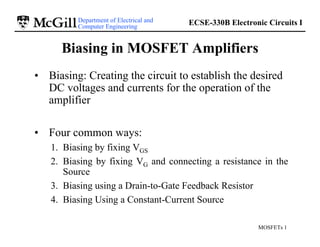
  • 1. Department of Electrical and Computer Engineering ECSE-330B Electronic Circuits I MOSFETs 1 Biasing in MOSFET Amplifiers • Biasing: Creating the circuit to establish the desired DC voltages and currents for the operation of the amplifier • Four common ways: 1. Biasing by fixing VGS 2. Biasing by fixing VG and connecting a resistance in the Source 3. Biasing using a Drain-to-Gate Feedback Resistor 4. Biasing Using a Constant-Current Source
  • 2. Department of Electrical and Computer Engineering ECSE-330B Electronic Circuits I MOSFETs 2 Biasing in MOSFET Amplifiers • Biasing by fixing VGS When the MOSFET device is changed (even using the same supplier), this method can result in a large variability in the value of ID. Devices 1 and 2 represent extremes among units of the same type. ( )2 2 1 t GS n D V V L W k I − ′ = ox n ox ox n n C t k μ ε μ = = ′ VDD -VEE VGG RG RD RS M1 VG VD VS
  • 3. Department of Electrical and Computer Engineering ECSE-330B Electronic Circuits I MOSFETs 3 Biasing in MOSFET Amplifiers • Biasing by fixing VG and connecting a resistance in the Source Degeneration Resistance
  • 4. Department of Electrical and Computer Engineering ECSE-330B Electronic Circuits I MOSFETs 4 Biasing in MOSFET Amplifiers • Biasing using a Drain-to-Gate Feedback Resistor Large Resistor
  • 5. Department of Electrical and Computer Engineering ECSE-330B Electronic Circuits I MOSFETs 5 Biasing in MOSFET Amplifiers • Biasing Using a Constant-Current Source Figure 4.33 (a) Biasing the MOSFET using a constant-current source I. (b) Implementation of the constant-current source I using a current mirror. Current Mirror Used in Integrated Circuits
  • 6. Department of Electrical and Computer Engineering ECSE-330B Electronic Circuits I MOSFETs 6 Current Mirror DC Analysis • The width and length (the W/L aspect ratio) and the parameters of the two transistors can be different • We can choose W/L freely • In this circuit, consider W/L of both MOSFETs are the same and transistors are identical. The Gate-Source voltages are also the same, then ( )2 1 1 2 1 t GS n REF V V L W k I − ′ = ( )2 1 1 2 1 t GS n V V L W k I − ′ = REF REF I I W L L W I I = = ⋅ = 1 1 1 1 1 W1 L1 VGS VGS + - - + W1 L1 I
  • 7. Department of Electrical and Computer Engineering ECSE-330B Electronic Circuits I MOSFETs 7 Current Mirror DC Analysis • Designing IREF R V V V I SS GS DD REF + − = ( )2 1 1 2 1 t GS n REF V V L W k I − ′ = • It is often needed to find the value of R in order to achieve a desired IREF
  • 8. Department of Electrical and Computer Engineering ECSE-330B Electronic Circuits I MOSFETs 8 Biasing of MOSFET Amplifier • 1- Intro to MOS Field Effect Transistor (MOSFET) • 2- NMOS FET • 3- PMOS FET • 4- DC Analysis of MOSFET Circuits • 5- MOSFET Amplifier • 6- MOSFET Small Signal Model • 7- MOSFET Integrated Circuits • 8- CSA, CGA, CDA • 9- CMOS Inverter & MOS Digital Logic
  • 9. Department of Electrical and Computer Engineering ECSE-330B Electronic Circuits I MOSFETs 9 MOSFET Design Space • Modern integrated circuits use MOSFETs extensively – Very high densities of transistors – up to 109 transistors/cm2 in some ULSI memory arrays. – Off-chip discrete resistors and capacitors are NOT commonly used – On-chip resistors and capacitors generally small – Multistage amplifiers are usually DC-coupled • Transistors used wherever possible to implement current sources, resistors, capacitors,
  • 10. Department of Electrical and Computer Engineering ECSE-330B Electronic Circuits I MOSFETs 10 Using MOSFETs to implement R’s and C’s • Resistors: Active Loads (large R’s) Diode-connected loads (small R’s) MOSFET Triode-Region (moderate R’s) • Capacitors Most obvious is the gate-body capacitor Can be used to have variable-capacitors as well • Current Mirrors
  • 11. Department of Electrical and Computer Engineering ECSE-330B Electronic Circuits I MOSFETs 11 MOSFET Active Loads • MOSFETs used as an active load for high resistances: – MOSFET is held in saturation with the source and gate held at a constant DC voltage – Drain connected to circuit vgs = 0 gmvgs = 0 D o I r ⋅ = λ 1 – ro is inversely proportional to ID Rin= ? Rin=ro
  • 12. Department of Electrical and Computer Engineering ECSE-330B Electronic Circuits I MOSFETs 12 Diode-Connected MOSFETs • A Diode connected MOSFET can be used to achieve small resistances: – The Drain is directly connected to Gate, and therefore it can only be operated in saturation (or cutoff) Source Absorption Theorem
  • 13. Department of Electrical and Computer Engineering ECSE-330B Electronic Circuits I MOSFETs 13 MOSFET Current Mirrors • Used extensively in MOSFET IC applications • Often ro,is neglected. Since there is no gate current, the drain currents of M1 and M2 are identical • In practice, IREF ≠ I due to finite ro. (Not included in EC1) VGS VGS + - - + 0 0 ( ) ) 1 ( 2 1 2 1 1 X t X n REF V V V L W k I λ + − ′ = 1 1 DS GS X V V V = = VX The current I will also depend on VDS2 I
  • 14. Department of Electrical and Computer Engineering ECSE-330B Electronic Circuits I MOSFETs 14 Current Mirror DC Analysis • The width and length (the W/L aspect ratio) of MOSFETs can be designed almost freely • Since the W/L of M1 and M2 need not be the same, the size ratios can affect current ratios ( )2 1 1 2 1 t GS n REF V V L W k I − ′ = ( )2 2 2 2 1 t GS n V V L W k I − ′ = 1 1 2 2 W L L W I I REF ⋅ = W1 L1 W2 L2 VGS VGS + - - + I
  • 15. Department of Electrical and Computer Engineering ECSE-330B Electronic Circuits I MOSFETs 15 Current Scaling (Steering) • Ratio of aspect ratios can be selected to achieve nearly any scale factor I/IREF W L W L W L W L Note: All gates are connected
  • 16. Department of Electrical and Computer Engineering ECSE-330B Electronic Circuits I MOSFETs 16 Current Mirroring – Pushing and Pulling
  • 17. Department of Electrical and Computer Engineering ECSE-330B Electronic Circuits I MOSFETs 17 Small Signal • Transistor M1 is diode connected and acts like a resistor to s.-s. ground. ro2
  • 18. Department of Electrical and Computer Engineering ECSE-330B Electronic Circuits I MOSFETs 18 Outline of Chapter 5 • 1- Intro to MOS Field Effect Transistor (MOSFET) • 2- NMOS FET • 3- PMOS FET • 4- DC Analysis of MOSFET Circuits • 5- MOSFET Amplifier • 6- MOSFET Small Signal Model • 7- MOSFET Integrated Circuits • 8- CSA, CGA, CDA • 9- CMOS Inverter & MOS Digital Logic
  • 19. Department of Electrical and Computer Engineering ECSE-330B Electronic Circuits I MOSFETs 19 DC and AC - Body-Effect / CLM Three types of analysis: Neglect AC Body-Effect & AC CLM / Neglect AC CLM Use AC Body-Effect Use AC Body-Effect / Use CLM Three types of analysis: Neglect DC Body-Effect & DC CLM / Neglect DC CLM Use DC Body-Effect Use DC Body-Effect / Use DC CLM DC Analysis AC Analysis (small-signal) Use whatever DC values for V and I in the small-signal analysis
  • 20. Department of Electrical and Computer Engineering ECSE-330B Electronic Circuits I MOSFETs 20 Common Source Amplifier (CSA) • Current source I implemented with current mirror. • Current mirror provides active load at drain • Source terminal grounded – no DC or AC Body effect
  • 21. Department of Electrical and Computer Engineering ECSE-330B Electronic Circuits I MOSFETs 21 CSA with Current Mirror CSA ro2
  • 22. Department of Electrical and Computer Engineering ECSE-330B Electronic Circuits I MOSFETs 22 CSA Small Signal Analysis • From MOSFET Current-Mirror: only ro2 appears in analysis i gs v v = 1 ( ) 1 2 1 1 gs o o m out v r r g v − = ( ) 2 1 1 o o m i out V r r g v v A − = =
  • 23. Department of Electrical and Computer Engineering ECSE-330B Electronic Circuits I MOSFETs 23 CSA Input/Output Resistance • Input Resistance • Output resistance 2 1 o o OUT r r R = vgs1 = 0 gm1vgs1 = 0 ∞ ⇒ IN R
  • 24. Department of Electrical and Computer Engineering ECSE-330B Electronic Circuits I MOSFETs 24 CSA Calculations • In practice, difficult to keep all transistors operating in saturation VOUT is hard to control, and sensitive to: W/L, VG, and CLM Ω = − = = = = = ′ = ′ = = = = − k R V V V V L W L W k k V V V V REF SS DD V A n V A p t t 1 2 , 5 40 , 50 125 50 1 01 . 0 1 1 2 2 2 1 1 2 1 μ μ λ λ V V V o V A m OUT G A k r m g V V mA I V V 100 52 . 38 192 . 5 855 . 3 596 . 2 567 . 2 1 − = Ω = = = = = Hand: SPICE: V V V OUT G A V V mA I V V 4 . 102 895 . 2 57 . 2 58 . 2 − = = = =
  • 25. Department of Electrical and Computer Engineering ECSE-330B Electronic Circuits I MOSFETs 25 Common Gate Amplifier (CGA) • A pMOS current mirror is used as IREF including the output resistance. • Since source terminal not at signal ground, the body effect is present. • The gate terminal held at a DC voltage. (AC Ground) Typically used as second stage of a multi-stage amplifier circuit
  • 26. Department of Electrical and Computer Engineering ECSE-330B Electronic Circuits I MOSFETs 26 CGA – DC Analysis • Current mirror is assumed to be ideal during the DC analysis, thus IREF=I • DC voltage at the source terminal (VS) must be obtained from driving the current IREF through the transistor. • This assumes that the input voltage source VI is set to zero • RI is part of the source voltage • Solve for VO, with VS and VG known, and including CLM ( ) ( ) [ ] S O t S G n V V V V V L W k I − ⋅ + − − ′ = λ 1 2 2 1
  • 27. Department of Electrical and Computer Engineering ECSE-330B Electronic Circuits I MOSFETs 27 CGA • Replace with a current source including output resistance ro2 Choice of analysis: Neglect AC Body-Effect & CLM / Neglect CLM Use AC Body-Effect Use AC Body-Effect / Use CLM ro2
  • 28. Department of Electrical and Computer Engineering ECSE-330B Electronic Circuits I MOSFETs 28 CGA – No Body Effect or CLM 2 o gs m o r v g v ⋅ − = I I m m gs v R g g v + − = 1 1 1 1 I m o I o V R g r v v A + = = 1 2 i=0 Non Inverting
  • 29. Department of Electrical and Computer Engineering ECSE-330B Electronic Circuits I MOSFETs 29 CGA – RIN & ROUT, No Body Effect or CLM 1 1 m IN g R = RIN ROUT 2 o OUT r R = vI = 0
  • 30. Department of Electrical and Computer Engineering ECSE-330B Electronic Circuits I MOSFETs 30 CGA – With Body Effect & no CLM ( ) 2 1 1 o x mb x m o r v g v g v + − = ( ) 2 1 1 o mb m x o V r g g v v A + = = x gs bs v v v − = = 1 1 ( ) 2 1 1 1 1 o bs mb gs m o r v g v g v + − = ( ) I IN IN o mb m i x x o i o total V R R R r g g v v v v v v A + ⋅ + = ⋅ = = − 2 Include RI and solve for total voltage gain in term of RIN RIN Solve at vx first: vX
  • 31. Department of Electrical and Computer Engineering ECSE-330B Electronic Circuits I MOSFETs 31 CGA – RIN With Body Effect & no CLM x mb m x v g g i ) ( 1 1 + = x gs bs v v v − = = 1 1 1 1 1 mb m IN g g R + = RIN iIN vX Neglect Input Voltage Source x mb m in v g g i ) ( 1 1 + = iX
  • 32. Department of Electrical and Computer Engineering ECSE-330B Electronic Circuits I MOSFETs 32 CGA - With Body Effect & CLM Neglect Input Voltage Source gs x v v − = 2 o x o r i v ⋅ = ( ) 1 1 1 o o x x mb m x r v v v g g i − + + = vX iX iX ( ) ⎟ ⎟ ⎠ ⎞ ⎜ ⎜ ⎝ ⎛ + + ⋅ = = 1 1 1 2 1 1 mb m o o o x o V g g r r r v v A
  • 33. Department of Electrical and Computer Engineering ECSE-330B Electronic Circuits I MOSFETs 33 CGA – RIN With Body Effect & CLM Neglect Input Voltage Source 2 o x o r i v ⋅ = ( ) 1 1 1 o o x x mb m x r v v v g g i − + + = 1 1 1 1 2 1 1 mb m o o o x x IN g g r r r i v R + + + = = RIN iX vX