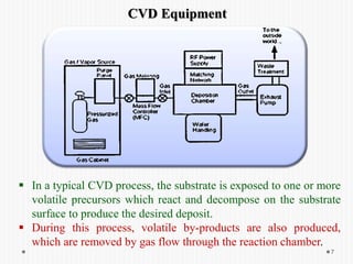
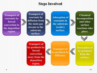
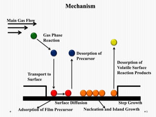
SlideShare a Scribd company logo
1 of 19
Download to read offline
CHEMICAL VAPOUR
DEPOSITION
Vijitha I.
JRF, CSIR-NIIST
Background
The formation of soot due to incomplete
oxidation of firewood since prehistoric
times is probably the oldest example of
deposition using CVD.
 Patent literature by de Lodyguine in 1893 on the deposition of W onto carbon
lamp filaments through the reduction of WCl6 by H2 lead to the industrial
exploitation of CVD.
CVD involves the dissociation and/or chemical
reactions of gaseous reactants in an activated (heat, light, plasma)
environment, followed by the formation of a stable solid product.
2
3
What is CVD?
Chemical vapor deposition (CVD) is a process whereby a solid
material is deposited from a vapor by a chemical reaction
occurring on or in the vicinity of a normally heated substrate
surface.
The solid material is obtained as a coating, a powder, or as single
crystals.
By varying the experimental conditions—substrate material,
substrate temperature, composition of the reaction gas mixture,
total pressure gas flows, etc.—materials with different properties
can be grown.
CVD is an example for Solid-Vapor Reaction.
Main Components of CVD Equipment
The role of this component is to generate vapour precursors and
then deliver to the reactor.
The design of the CVD reactor depends on whether the starting
material is solid, liquid or gas.
The sublimation of a solid precursor depends on surface area of the
solid and contact time.
Liquid sources often use a bubbler to vaporise the reactants, and a
carrier gas (reactive gases such as H2 or inert gases such as Ar) to
transport the vaporised reactants into the reactor.
4
1. Chemical vapour precursor supply system
2. CVD reactors
Hot-wall reactor:
 In this the substrate (wafer) and the walls of the reactor are heated, i.e. a
homogeneous temperature is maintained inside the reaction chamber.
Disadvantage of hot-wall reactor
Contamination
Cold-wall reactor:
 This reactors uses heating systems that minimize the heating up of the reactor
walls while the wafer is being heated up. The temperature is not homogeneous
inside the reaction chamber.
Disadvantage of cold-wall reactor
It is difficult to get a uniform layer of the film.
5
3. The effluent gas handling system
This component consists of a neutralizing part for the exhaust
gases, and/or a vacuum system to provide the required reduced
pressure for the CVD process that performs at low pressure or high
vacuum during deposition.
The unreacted precursors and corrosive by-products such as HCl
are neutralised or trapped using a liquid nitrogen trap.
Inflammable gases such as hydrogen are burned off.
Unreacted expensive precursors may be collected at the outlet and
recycled.
6
7
CVD Equipment
 In a typical CVD process, the substrate is exposed to one or more
volatile precursors which react and decompose on the substrate
surface to produce the desired deposit.
 During this process, volatile by-products are also produced,
which are removed by gas flow through the reaction chamber.
Steps Involved
8
Transport of
reactants by
forced
convection to
the deposition
region.
Desorption of
by-products
from the
surface.
Transport of
by-products by
diffusion.
Transport of
by-products by
forced
convection
away from the
deposition
region.
Transport of
reactants by
diffusion from
the main gas
stream to the
substrate
surface.
Adsorption of
reactants in
the substrate
(wafer)
surface.
Chemical
decomposition
and other
surface
reactions take
place.
9
Mechanism
Main Gas Flow
Gas Phase
Reaction
Transport to
Surface
Surface Diffusion
Adsorption of Film Precursor
Step Growth
Nucleation and Island Growth
Desorption of
Precursor
Desorption of
Volatile Surface
Reaction Products
10
Types
CVD
LPCVD
PECVD
MOCVD
PHCVD
APCVD
Atmospheric
Pressure CVD
Low Pressure CVD
Metal Organic
CVD
Plasma
Enhanced CVD
Photon (Laser)
Induced CVD
11
Atmospheric pressure chemical vapour deposition (APCVD)
 It works at atmospheric pressure.
 It is used to deposit a layer of material typically several
micrometers thick onto a wafer or other type of substrate.
 It is also used as a surface finishing process for items such as tools
and turbine blades to improve lifetime and performance.
 Since a vacuum system is not required, APCVD systems have a
relatively low operating cost.
 APCVD has inherently poor utilization.
 APCVD is extremely susceptible to oxidation due to the greater
gas density and residence times.
12
 LPCVD coatings exhibit excellent uniformity, high purity, and
good step coverage.
 It works at sub-atmospheric pressures. Reduced pressures tend
to reduce unwanted gas-phase reactions and improve film
uniformity across the wafer.
 The lower pressure increases the precursor diffusion through the
gas and the mass transfer rate of the gaseous reactants becomes
higher than the surface-reaction rate.
 The pressure for LPCVD is usually around 10-1000 Pa while
standard atmospheric pressure is 101,325 Pa.
Low pressure chemical vapour deposition (LPCVD)
Metal-organic chemical vapour deposition (MOCVD)
 Metal-organic compounds are used as molecular precursors to
deposit, a wide variety of thin film materials for new industrial
applications.
 The great advantage of MOCVD precursors are their high
volatility at moderate to low temperatures, therefore reaction
temperatures are lower (750 to 1100 K) than conventional CVD.
 The main disadvantages are the precursors tend to be very
expensive and are very volatile. When reactive liquids are used
they require accurate pressure control and are difficult to purify.
13
14
Laser chemical vapour deposition (LCVD)
 LCVD uses a focussed laser beam to heat the substrate.
 It also has the ability to locally heat a part of the substrate while
passing the reactant gas, thereby inducing film deposition by
locally driving the CVD reaction at the surface.
 It is used to deposit microscale solid patterns or three
dimensional structures on the surface of a substrate by a
localized, single step process.
Plasma-enhanced chemical vapour deposition (PECVD)
 PECVD is used to deposit SiO2, Si3N4 (SixNy), SixOyNz and
amorphous Si films.
 Plasma can be used to decompose a molecule that will not
decompose at a reasonable elevated temperature.
 It can be used to decompose a thermally unstable molecule but
at a much lower temperature.
 In plasma CVD substrates that cannot tolerate high
temperatures, such as polymers, can be used, where substrate
temperatures range from 100 to 500°C.
15
16
Advantages
 CVD films are generally quite conformal, i.e., the ability of a film
to uniformly coat a topographically complex substrate.
 Versatile –any element or compound can be deposited.
 High purity can be obtained.
 High density – nearly 100% of theoretical value.
 CVD films are harder than similar materials produced using
conventional ceramic fabrication processes.
 Material formation well below the melting point.
 Economical in production, since many parts can be coated at the
same time.
17
Disadvantages
o Chemical and safety hazards caused by the use of toxic,
corrosive, flammable and/or explosive precursor. Therefore extra
steps have to be taken in the handling of the precursors and in
the treatment of the reactor exhaust.
o High deposition temperatures (often greater than 600 °C) are
often unsuitable for structures already fabricated on substrates.
o Restrictions on the kind of substrates that can be coated.
o It leads to stresses in films deposited on materials with different
thermal expansion coefficients, which can cause mechanical
instabilities in the deposited films.
18
Applications
 Coatings – Coatings for a variety of applications such as wear
resistance, corrosion resistance, high temperature protection.
 Semiconductors and related devices – Integrated circuits, sensors
and optoelectronic devices.
 Fiber optics – for telecommunication.
 Used in the microelectronics industry to make films serving as
dielectrics, conductors, passivation layers, oxidation barriers, and
epitaxial layers.
19

More Related Content

What's hot

Kimyasal Buhar Biriktirme (CVD)
Kimyasal Buhar Biriktirme (CVD)Kimyasal Buhar Biriktirme (CVD)
Kimyasal Buhar Biriktirme (CVD)Zümrüt Varol
 
FABRICATION PROCESS
FABRICATION PROCESSFABRICATION PROCESS
FABRICATION PROCESSKUNAL RANA
 
Chemical Vapour Deposition
Chemical Vapour DepositionChemical Vapour Deposition
Chemical Vapour Depositionjitendrahemwani
 
Estereotaxia - O que o técnico precisa saber
Estereotaxia - O que o técnico precisa saberEstereotaxia - O que o técnico precisa saber
Estereotaxia - O que o técnico precisa saberLucas Radicchi
 
photonic crystal.pptx
photonic crystal.pptxphotonic crystal.pptx
photonic crystal.pptxDanh Bich Do
 
Epitaxial Crystal Growth: Methods & Analysis
Epitaxial Crystal Growth: Methods & Analysis Epitaxial Crystal Growth: Methods & Analysis
Epitaxial Crystal Growth: Methods & Analysis KaŃnán RãjËev
 
Review of physical vapor deposition coatings
Review of physical vapor deposition coatingsReview of physical vapor deposition coatings
Review of physical vapor deposition coatingsRathiram Naik
 
A.F. Ismail (presentation)
A.F. Ismail (presentation)A.F. Ismail (presentation)
A.F. Ismail (presentation)Elektro_UMBO
 
Nano technology by smitkapdiya
Nano technology by smitkapdiyaNano technology by smitkapdiya
Nano technology by smitkapdiyaSmit Kapadiya
 
Projection lithography
Projection lithographyProjection lithography
Projection lithographyMirza Baig
 
Chemical Vaour Deposition & Physical Vapour Deposition techniques.
Chemical Vaour Deposition & Physical Vapour Deposition techniques.Chemical Vaour Deposition & Physical Vapour Deposition techniques.
Chemical Vaour Deposition & Physical Vapour Deposition techniques.Tapan Patel
 
CMOS FABRICATION AND TECHNIQUES
CMOS FABRICATION AND TECHNIQUESCMOS FABRICATION AND TECHNIQUES
CMOS FABRICATION AND TECHNIQUESAbhishek Sur
 
Chemical Vapour Deposition
Chemical Vapour DepositionChemical Vapour Deposition
Chemical Vapour Depositionaroosa khan
 
Fiber fabrications
Fiber fabricationsFiber fabrications
Fiber fabricationsSagar Adroja
 
High-Speed Single-Photon SPAD Camera
High-Speed Single-Photon SPAD CameraHigh-Speed Single-Photon SPAD Camera
High-Speed Single-Photon SPAD CameraFabrizio Guerrieri
 

What's hot (20)

Epitaxy
EpitaxyEpitaxy
Epitaxy
 
Kimyasal Buhar Biriktirme (CVD)
Kimyasal Buhar Biriktirme (CVD)Kimyasal Buhar Biriktirme (CVD)
Kimyasal Buhar Biriktirme (CVD)
 
FABRICATION PROCESS
FABRICATION PROCESSFABRICATION PROCESS
FABRICATION PROCESS
 
Chemical Vapour Deposition
Chemical Vapour DepositionChemical Vapour Deposition
Chemical Vapour Deposition
 
Estereotaxia - O que o técnico precisa saber
Estereotaxia - O que o técnico precisa saberEstereotaxia - O que o técnico precisa saber
Estereotaxia - O que o técnico precisa saber
 
photonic crystal.pptx
photonic crystal.pptxphotonic crystal.pptx
photonic crystal.pptx
 
Epitaxial Crystal Growth: Methods & Analysis
Epitaxial Crystal Growth: Methods & Analysis Epitaxial Crystal Growth: Methods & Analysis
Epitaxial Crystal Growth: Methods & Analysis
 
Review of physical vapor deposition coatings
Review of physical vapor deposition coatingsReview of physical vapor deposition coatings
Review of physical vapor deposition coatings
 
A.F. Ismail (presentation)
A.F. Ismail (presentation)A.F. Ismail (presentation)
A.F. Ismail (presentation)
 
Nano technology by smitkapdiya
Nano technology by smitkapdiyaNano technology by smitkapdiya
Nano technology by smitkapdiya
 
Projection lithography
Projection lithographyProjection lithography
Projection lithography
 
Lecture 13 2013_
Lecture 13 2013_Lecture 13 2013_
Lecture 13 2013_
 
Chemical Vaour Deposition & Physical Vapour Deposition techniques.
Chemical Vaour Deposition & Physical Vapour Deposition techniques.Chemical Vaour Deposition & Physical Vapour Deposition techniques.
Chemical Vaour Deposition & Physical Vapour Deposition techniques.
 
2.1 P Fotolitografia
2.1   P  Fotolitografia2.1   P  Fotolitografia
2.1 P Fotolitografia
 
CMOS FABRICATION AND TECHNIQUES
CMOS FABRICATION AND TECHNIQUESCMOS FABRICATION AND TECHNIQUES
CMOS FABRICATION AND TECHNIQUES
 
Chemical Vapour Deposition
Chemical Vapour DepositionChemical Vapour Deposition
Chemical Vapour Deposition
 
Immersion lithography
Immersion lithographyImmersion lithography
Immersion lithography
 
Fiber fabrications
Fiber fabricationsFiber fabrications
Fiber fabrications
 
THIN FILMS.pdf
THIN FILMS.pdfTHIN FILMS.pdf
THIN FILMS.pdf
 
High-Speed Single-Photon SPAD Camera
High-Speed Single-Photon SPAD CameraHigh-Speed Single-Photon SPAD Camera
High-Speed Single-Photon SPAD Camera
 

Similar to Ed_ppt .pdf

Chemical vapor deposition and its types 120589
Chemical vapor deposition and its types 120589Chemical vapor deposition and its types 120589
Chemical vapor deposition and its types 120589Adnan Majeed
 
Chemical vapour deposition
Chemical vapour depositionChemical vapour deposition
Chemical vapour depositionSethu Ram
 
chemicalvapourdeposition-120430095030-phpapp02.pptx
chemicalvapourdeposition-120430095030-phpapp02.pptxchemicalvapourdeposition-120430095030-phpapp02.pptx
chemicalvapourdeposition-120430095030-phpapp02.pptxssuserdcfc6d
 
Ic technology- chemical vapour deposition and epitaxial layer growth
Ic technology- chemical vapour deposition and epitaxial layer growthIc technology- chemical vapour deposition and epitaxial layer growth
Ic technology- chemical vapour deposition and epitaxial layer growthkriticka sharma
 
Chemical Vapour Deposition (CVD).pdf
Chemical Vapour Deposition (CVD).pdfChemical Vapour Deposition (CVD).pdf
Chemical Vapour Deposition (CVD).pdfSanDeepSharma926061
 
Cvd & pvd by shreya
Cvd & pvd by shreyaCvd & pvd by shreya
Cvd & pvd by shreyaShreya Modi
 
Thinfilms and nanomaterials_Modified October 2020.pptx
Thinfilms and nanomaterials_Modified October 2020.pptxThinfilms and nanomaterials_Modified October 2020.pptx
Thinfilms and nanomaterials_Modified October 2020.pptxhappycocoman
 
Low Pressure Chemical Vapour Deposition
Low Pressure Chemical Vapour DepositionLow Pressure Chemical Vapour Deposition
Low Pressure Chemical Vapour DepositionSudhanshu Janwadkar
 
thin films Engineering Chemistry Year 1.pptx
thin films Engineering Chemistry Year 1.pptxthin films Engineering Chemistry Year 1.pptx
thin films Engineering Chemistry Year 1.pptxhappycocoman
 
6_2020_04_11!06_48_32_AM.pptx
6_2020_04_11!06_48_32_AM.pptx6_2020_04_11!06_48_32_AM.pptx
6_2020_04_11!06_48_32_AM.pptxShamimAkhter52
 
Chemical vapor deposition (cvd)
Chemical vapor deposition (cvd)Chemical vapor deposition (cvd)
Chemical vapor deposition (cvd)Khalid Raza
 
NANO Physics ppt ---2017
 NANO Physics ppt ---2017  NANO Physics ppt ---2017
NANO Physics ppt ---2017 ANANT VYAS
 
anti reflective coatings on the solar photo voltaic panel's
anti reflective coatings on the solar photo voltaic panel'santi reflective coatings on the solar photo voltaic panel's
anti reflective coatings on the solar photo voltaic panel'sRajneesh Gautam
 
Vapor deposition (CVD & PVD) on tools
Vapor deposition (CVD & PVD) on toolsVapor deposition (CVD & PVD) on tools
Vapor deposition (CVD & PVD) on toolsMuhammad Umair Akram
 

Similar to Ed_ppt .pdf (20)

Chemical vapor deposition and its types 120589
Chemical vapor deposition and its types 120589Chemical vapor deposition and its types 120589
Chemical vapor deposition and its types 120589
 
Chemical vapour deposition
Chemical vapour depositionChemical vapour deposition
Chemical vapour deposition
 
chemicalvapourdeposition-120430095030-phpapp02.pptx
chemicalvapourdeposition-120430095030-phpapp02.pptxchemicalvapourdeposition-120430095030-phpapp02.pptx
chemicalvapourdeposition-120430095030-phpapp02.pptx
 
Ic technology- chemical vapour deposition and epitaxial layer growth
Ic technology- chemical vapour deposition and epitaxial layer growthIc technology- chemical vapour deposition and epitaxial layer growth
Ic technology- chemical vapour deposition and epitaxial layer growth
 
Chemical Vapour Deposition (CVD).pdf
Chemical Vapour Deposition (CVD).pdfChemical Vapour Deposition (CVD).pdf
Chemical Vapour Deposition (CVD).pdf
 
Cvd & pvd by shreya
Cvd & pvd by shreyaCvd & pvd by shreya
Cvd & pvd by shreya
 
PVD,CVD,AFM.ppt
PVD,CVD,AFM.pptPVD,CVD,AFM.ppt
PVD,CVD,AFM.ppt
 
Chemical vapour deposition
Chemical vapour depositionChemical vapour deposition
Chemical vapour deposition
 
Thinfilms and nanomaterials_Modified October 2020.pptx
Thinfilms and nanomaterials_Modified October 2020.pptxThinfilms and nanomaterials_Modified October 2020.pptx
Thinfilms and nanomaterials_Modified October 2020.pptx
 
Subrat cvd
Subrat cvdSubrat cvd
Subrat cvd
 
Low Pressure Chemical Vapour Deposition
Low Pressure Chemical Vapour DepositionLow Pressure Chemical Vapour Deposition
Low Pressure Chemical Vapour Deposition
 
thin films Engineering Chemistry Year 1.pptx
thin films Engineering Chemistry Year 1.pptxthin films Engineering Chemistry Year 1.pptx
thin films Engineering Chemistry Year 1.pptx
 
6_2020_04_11!06_48_32_AM.pptx
6_2020_04_11!06_48_32_AM.pptx6_2020_04_11!06_48_32_AM.pptx
6_2020_04_11!06_48_32_AM.pptx
 
Chemical vapor deposition (cvd)
Chemical vapor deposition (cvd)Chemical vapor deposition (cvd)
Chemical vapor deposition (cvd)
 
By final
By finalBy final
By final
 
By final
By finalBy final
By final
 
NANO Physics ppt ---2017
 NANO Physics ppt ---2017  NANO Physics ppt ---2017
NANO Physics ppt ---2017
 
Nano materials
Nano materialsNano materials
Nano materials
 
anti reflective coatings on the solar photo voltaic panel's
anti reflective coatings on the solar photo voltaic panel'santi reflective coatings on the solar photo voltaic panel's
anti reflective coatings on the solar photo voltaic panel's
 
Vapor deposition (CVD & PVD) on tools
Vapor deposition (CVD & PVD) on toolsVapor deposition (CVD & PVD) on tools
Vapor deposition (CVD & PVD) on tools
 

Recently uploaded

Best VIP Call Girls Noida Sector 44 Call Me: 8448380779
Best VIP Call Girls Noida Sector 44 Call Me: 8448380779Best VIP Call Girls Noida Sector 44 Call Me: 8448380779
Best VIP Call Girls Noida Sector 44 Call Me: 8448380779Delhi Call girls
 
Best VIP Call Girls Noida Sector 47 Call Me: 8448380779
Best VIP Call Girls Noida Sector 47 Call Me: 8448380779Best VIP Call Girls Noida Sector 47 Call Me: 8448380779
Best VIP Call Girls Noida Sector 47 Call Me: 8448380779Delhi Call girls
 
The_Canvas_of_Creative_Mastery_Newsletter_April_2024_Version.pdf
The_Canvas_of_Creative_Mastery_Newsletter_April_2024_Version.pdfThe_Canvas_of_Creative_Mastery_Newsletter_April_2024_Version.pdf
The_Canvas_of_Creative_Mastery_Newsletter_April_2024_Version.pdfAmirYakdi
 
VIP College Call Girls Gorakhpur Bhavna 8250192130 Independent Escort Service...
VIP College Call Girls Gorakhpur Bhavna 8250192130 Independent Escort Service...VIP College Call Girls Gorakhpur Bhavna 8250192130 Independent Escort Service...
VIP College Call Girls Gorakhpur Bhavna 8250192130 Independent Escort Service...Suhani Kapoor
 
Design Portfolio - 2024 - William Vickery
Design Portfolio - 2024 - William VickeryDesign Portfolio - 2024 - William Vickery
Design Portfolio - 2024 - William VickeryWilliamVickery6
 
SD_The MATATAG Curriculum Training Design.pptx
SD_The MATATAG Curriculum Training Design.pptxSD_The MATATAG Curriculum Training Design.pptx
SD_The MATATAG Curriculum Training Design.pptxjanettecruzeiro1
 
Abu Dhabi Call Girls O58993O4O2 Call Girls in Abu Dhabi`
Abu Dhabi Call Girls O58993O4O2 Call Girls in Abu Dhabi`Abu Dhabi Call Girls O58993O4O2 Call Girls in Abu Dhabi`
Abu Dhabi Call Girls O58993O4O2 Call Girls in Abu Dhabi`dajasot375
 
VIP Call Girl Amravati Aashi 8250192130 Independent Escort Service Amravati
VIP Call Girl Amravati Aashi 8250192130 Independent Escort Service AmravatiVIP Call Girl Amravati Aashi 8250192130 Independent Escort Service Amravati
VIP Call Girl Amravati Aashi 8250192130 Independent Escort Service AmravatiSuhani Kapoor
 
How to Be Famous in your Field just visit our Site
How to Be Famous in your Field just visit our SiteHow to Be Famous in your Field just visit our Site
How to Be Famous in your Field just visit our Sitegalleryaagency
 
VIP Russian Call Girls in Gorakhpur Deepika 8250192130 Independent Escort Ser...
VIP Russian Call Girls in Gorakhpur Deepika 8250192130 Independent Escort Ser...VIP Russian Call Girls in Gorakhpur Deepika 8250192130 Independent Escort Ser...
VIP Russian Call Girls in Gorakhpur Deepika 8250192130 Independent Escort Ser...Suhani Kapoor
 
Cheap Rate ➥8448380779 ▻Call Girls In Iffco Chowk Gurgaon
Cheap Rate ➥8448380779 ▻Call Girls In Iffco Chowk GurgaonCheap Rate ➥8448380779 ▻Call Girls In Iffco Chowk Gurgaon
Cheap Rate ➥8448380779 ▻Call Girls In Iffco Chowk GurgaonDelhi Call girls
 
NO1 Trending kala jadu Love Marriage Black Magic Punjab Powerful Black Magic ...
NO1 Trending kala jadu Love Marriage Black Magic Punjab Powerful Black Magic ...NO1 Trending kala jadu Love Marriage Black Magic Punjab Powerful Black Magic ...
NO1 Trending kala jadu Love Marriage Black Magic Punjab Powerful Black Magic ...Amil baba
 
CALL ON ➥8923113531 🔝Call Girls Aminabad Lucknow best Night Fun service
CALL ON ➥8923113531 🔝Call Girls Aminabad Lucknow best Night Fun serviceCALL ON ➥8923113531 🔝Call Girls Aminabad Lucknow best Night Fun service
CALL ON ➥8923113531 🔝Call Girls Aminabad Lucknow best Night Fun serviceanilsa9823
 
Cheap Rate Call girls Malviya Nagar 9205541914 shot 1500 night
Cheap Rate Call girls Malviya Nagar 9205541914 shot 1500 nightCheap Rate Call girls Malviya Nagar 9205541914 shot 1500 night
Cheap Rate Call girls Malviya Nagar 9205541914 shot 1500 nightDelhi Call girls
 
Recommendable # 971589162217 # philippine Young Call Girls in Dubai By Marina...
Recommendable # 971589162217 # philippine Young Call Girls in Dubai By Marina...Recommendable # 971589162217 # philippine Young Call Girls in Dubai By Marina...
Recommendable # 971589162217 # philippine Young Call Girls in Dubai By Marina...home
 
VIP Call Girls Service Mehdipatnam Hyderabad Call +91-8250192130
VIP Call Girls Service Mehdipatnam Hyderabad Call +91-8250192130VIP Call Girls Service Mehdipatnam Hyderabad Call +91-8250192130
VIP Call Girls Service Mehdipatnam Hyderabad Call +91-8250192130Suhani Kapoor
 
VIP Call Girls Bhiwandi Ananya 8250192130 Independent Escort Service Bhiwandi
VIP Call Girls Bhiwandi Ananya 8250192130 Independent Escort Service BhiwandiVIP Call Girls Bhiwandi Ananya 8250192130 Independent Escort Service Bhiwandi
VIP Call Girls Bhiwandi Ananya 8250192130 Independent Escort Service BhiwandiSuhani Kapoor
 
VIP Call Girls Service Bhagyanagar Hyderabad Call +91-8250192130
VIP Call Girls Service Bhagyanagar Hyderabad Call +91-8250192130VIP Call Girls Service Bhagyanagar Hyderabad Call +91-8250192130
VIP Call Girls Service Bhagyanagar Hyderabad Call +91-8250192130Suhani Kapoor
 
Kindergarten Assessment Questions Via LessonUp
Kindergarten Assessment Questions Via LessonUpKindergarten Assessment Questions Via LessonUp
Kindergarten Assessment Questions Via LessonUpmainac1
 

Recently uploaded (20)

Best VIP Call Girls Noida Sector 44 Call Me: 8448380779
Best VIP Call Girls Noida Sector 44 Call Me: 8448380779Best VIP Call Girls Noida Sector 44 Call Me: 8448380779
Best VIP Call Girls Noida Sector 44 Call Me: 8448380779
 
Best VIP Call Girls Noida Sector 47 Call Me: 8448380779
Best VIP Call Girls Noida Sector 47 Call Me: 8448380779Best VIP Call Girls Noida Sector 47 Call Me: 8448380779
Best VIP Call Girls Noida Sector 47 Call Me: 8448380779
 
The_Canvas_of_Creative_Mastery_Newsletter_April_2024_Version.pdf
The_Canvas_of_Creative_Mastery_Newsletter_April_2024_Version.pdfThe_Canvas_of_Creative_Mastery_Newsletter_April_2024_Version.pdf
The_Canvas_of_Creative_Mastery_Newsletter_April_2024_Version.pdf
 
VIP College Call Girls Gorakhpur Bhavna 8250192130 Independent Escort Service...
VIP College Call Girls Gorakhpur Bhavna 8250192130 Independent Escort Service...VIP College Call Girls Gorakhpur Bhavna 8250192130 Independent Escort Service...
VIP College Call Girls Gorakhpur Bhavna 8250192130 Independent Escort Service...
 
Design Portfolio - 2024 - William Vickery
Design Portfolio - 2024 - William VickeryDesign Portfolio - 2024 - William Vickery
Design Portfolio - 2024 - William Vickery
 
SD_The MATATAG Curriculum Training Design.pptx
SD_The MATATAG Curriculum Training Design.pptxSD_The MATATAG Curriculum Training Design.pptx
SD_The MATATAG Curriculum Training Design.pptx
 
Abu Dhabi Call Girls O58993O4O2 Call Girls in Abu Dhabi`
Abu Dhabi Call Girls O58993O4O2 Call Girls in Abu Dhabi`Abu Dhabi Call Girls O58993O4O2 Call Girls in Abu Dhabi`
Abu Dhabi Call Girls O58993O4O2 Call Girls in Abu Dhabi`
 
VIP Call Girl Amravati Aashi 8250192130 Independent Escort Service Amravati
VIP Call Girl Amravati Aashi 8250192130 Independent Escort Service AmravatiVIP Call Girl Amravati Aashi 8250192130 Independent Escort Service Amravati
VIP Call Girl Amravati Aashi 8250192130 Independent Escort Service Amravati
 
How to Be Famous in your Field just visit our Site
How to Be Famous in your Field just visit our SiteHow to Be Famous in your Field just visit our Site
How to Be Famous in your Field just visit our Site
 
VIP Russian Call Girls in Gorakhpur Deepika 8250192130 Independent Escort Ser...
VIP Russian Call Girls in Gorakhpur Deepika 8250192130 Independent Escort Ser...VIP Russian Call Girls in Gorakhpur Deepika 8250192130 Independent Escort Ser...
VIP Russian Call Girls in Gorakhpur Deepika 8250192130 Independent Escort Ser...
 
Cheap Rate ➥8448380779 ▻Call Girls In Iffco Chowk Gurgaon
Cheap Rate ➥8448380779 ▻Call Girls In Iffco Chowk GurgaonCheap Rate ➥8448380779 ▻Call Girls In Iffco Chowk Gurgaon
Cheap Rate ➥8448380779 ▻Call Girls In Iffco Chowk Gurgaon
 
young call girls in Vivek Vihar🔝 9953056974 🔝 Delhi escort Service
young call girls in Vivek Vihar🔝 9953056974 🔝 Delhi escort Serviceyoung call girls in Vivek Vihar🔝 9953056974 🔝 Delhi escort Service
young call girls in Vivek Vihar🔝 9953056974 🔝 Delhi escort Service
 
NO1 Trending kala jadu Love Marriage Black Magic Punjab Powerful Black Magic ...
NO1 Trending kala jadu Love Marriage Black Magic Punjab Powerful Black Magic ...NO1 Trending kala jadu Love Marriage Black Magic Punjab Powerful Black Magic ...
NO1 Trending kala jadu Love Marriage Black Magic Punjab Powerful Black Magic ...
 
CALL ON ➥8923113531 🔝Call Girls Aminabad Lucknow best Night Fun service
CALL ON ➥8923113531 🔝Call Girls Aminabad Lucknow best Night Fun serviceCALL ON ➥8923113531 🔝Call Girls Aminabad Lucknow best Night Fun service
CALL ON ➥8923113531 🔝Call Girls Aminabad Lucknow best Night Fun service
 
Cheap Rate Call girls Malviya Nagar 9205541914 shot 1500 night
Cheap Rate Call girls Malviya Nagar 9205541914 shot 1500 nightCheap Rate Call girls Malviya Nagar 9205541914 shot 1500 night
Cheap Rate Call girls Malviya Nagar 9205541914 shot 1500 night
 
Recommendable # 971589162217 # philippine Young Call Girls in Dubai By Marina...
Recommendable # 971589162217 # philippine Young Call Girls in Dubai By Marina...Recommendable # 971589162217 # philippine Young Call Girls in Dubai By Marina...
Recommendable # 971589162217 # philippine Young Call Girls in Dubai By Marina...
 
VIP Call Girls Service Mehdipatnam Hyderabad Call +91-8250192130
VIP Call Girls Service Mehdipatnam Hyderabad Call +91-8250192130VIP Call Girls Service Mehdipatnam Hyderabad Call +91-8250192130
VIP Call Girls Service Mehdipatnam Hyderabad Call +91-8250192130
 
VIP Call Girls Bhiwandi Ananya 8250192130 Independent Escort Service Bhiwandi
VIP Call Girls Bhiwandi Ananya 8250192130 Independent Escort Service BhiwandiVIP Call Girls Bhiwandi Ananya 8250192130 Independent Escort Service Bhiwandi
VIP Call Girls Bhiwandi Ananya 8250192130 Independent Escort Service Bhiwandi
 
VIP Call Girls Service Bhagyanagar Hyderabad Call +91-8250192130
VIP Call Girls Service Bhagyanagar Hyderabad Call +91-8250192130VIP Call Girls Service Bhagyanagar Hyderabad Call +91-8250192130
VIP Call Girls Service Bhagyanagar Hyderabad Call +91-8250192130
 
Kindergarten Assessment Questions Via LessonUp
Kindergarten Assessment Questions Via LessonUpKindergarten Assessment Questions Via LessonUp
Kindergarten Assessment Questions Via LessonUp
 

Ed_ppt .pdf

  • 2. Background The formation of soot due to incomplete oxidation of firewood since prehistoric times is probably the oldest example of deposition using CVD.  Patent literature by de Lodyguine in 1893 on the deposition of W onto carbon lamp filaments through the reduction of WCl6 by H2 lead to the industrial exploitation of CVD. CVD involves the dissociation and/or chemical reactions of gaseous reactants in an activated (heat, light, plasma) environment, followed by the formation of a stable solid product. 2
  • 3. 3 What is CVD? Chemical vapor deposition (CVD) is a process whereby a solid material is deposited from a vapor by a chemical reaction occurring on or in the vicinity of a normally heated substrate surface. The solid material is obtained as a coating, a powder, or as single crystals. By varying the experimental conditions—substrate material, substrate temperature, composition of the reaction gas mixture, total pressure gas flows, etc.—materials with different properties can be grown. CVD is an example for Solid-Vapor Reaction.
  • 4. Main Components of CVD Equipment The role of this component is to generate vapour precursors and then deliver to the reactor. The design of the CVD reactor depends on whether the starting material is solid, liquid or gas. The sublimation of a solid precursor depends on surface area of the solid and contact time. Liquid sources often use a bubbler to vaporise the reactants, and a carrier gas (reactive gases such as H2 or inert gases such as Ar) to transport the vaporised reactants into the reactor. 4 1. Chemical vapour precursor supply system
  • 5. 2. CVD reactors Hot-wall reactor:  In this the substrate (wafer) and the walls of the reactor are heated, i.e. a homogeneous temperature is maintained inside the reaction chamber. Disadvantage of hot-wall reactor Contamination Cold-wall reactor:  This reactors uses heating systems that minimize the heating up of the reactor walls while the wafer is being heated up. The temperature is not homogeneous inside the reaction chamber. Disadvantage of cold-wall reactor It is difficult to get a uniform layer of the film. 5
  • 6. 3. The effluent gas handling system This component consists of a neutralizing part for the exhaust gases, and/or a vacuum system to provide the required reduced pressure for the CVD process that performs at low pressure or high vacuum during deposition. The unreacted precursors and corrosive by-products such as HCl are neutralised or trapped using a liquid nitrogen trap. Inflammable gases such as hydrogen are burned off. Unreacted expensive precursors may be collected at the outlet and recycled. 6
  • 7. 7 CVD Equipment  In a typical CVD process, the substrate is exposed to one or more volatile precursors which react and decompose on the substrate surface to produce the desired deposit.  During this process, volatile by-products are also produced, which are removed by gas flow through the reaction chamber.
  • 8. Steps Involved 8 Transport of reactants by forced convection to the deposition region. Desorption of by-products from the surface. Transport of by-products by diffusion. Transport of by-products by forced convection away from the deposition region. Transport of reactants by diffusion from the main gas stream to the substrate surface. Adsorption of reactants in the substrate (wafer) surface. Chemical decomposition and other surface reactions take place.
  • 9. 9 Mechanism Main Gas Flow Gas Phase Reaction Transport to Surface Surface Diffusion Adsorption of Film Precursor Step Growth Nucleation and Island Growth Desorption of Precursor Desorption of Volatile Surface Reaction Products
  • 10. 10 Types CVD LPCVD PECVD MOCVD PHCVD APCVD Atmospheric Pressure CVD Low Pressure CVD Metal Organic CVD Plasma Enhanced CVD Photon (Laser) Induced CVD
  • 11. 11 Atmospheric pressure chemical vapour deposition (APCVD)  It works at atmospheric pressure.  It is used to deposit a layer of material typically several micrometers thick onto a wafer or other type of substrate.  It is also used as a surface finishing process for items such as tools and turbine blades to improve lifetime and performance.  Since a vacuum system is not required, APCVD systems have a relatively low operating cost.  APCVD has inherently poor utilization.  APCVD is extremely susceptible to oxidation due to the greater gas density and residence times.
  • 12. 12  LPCVD coatings exhibit excellent uniformity, high purity, and good step coverage.  It works at sub-atmospheric pressures. Reduced pressures tend to reduce unwanted gas-phase reactions and improve film uniformity across the wafer.  The lower pressure increases the precursor diffusion through the gas and the mass transfer rate of the gaseous reactants becomes higher than the surface-reaction rate.  The pressure for LPCVD is usually around 10-1000 Pa while standard atmospheric pressure is 101,325 Pa. Low pressure chemical vapour deposition (LPCVD)
  • 13. Metal-organic chemical vapour deposition (MOCVD)  Metal-organic compounds are used as molecular precursors to deposit, a wide variety of thin film materials for new industrial applications.  The great advantage of MOCVD precursors are their high volatility at moderate to low temperatures, therefore reaction temperatures are lower (750 to 1100 K) than conventional CVD.  The main disadvantages are the precursors tend to be very expensive and are very volatile. When reactive liquids are used they require accurate pressure control and are difficult to purify. 13
  • 14. 14 Laser chemical vapour deposition (LCVD)  LCVD uses a focussed laser beam to heat the substrate.  It also has the ability to locally heat a part of the substrate while passing the reactant gas, thereby inducing film deposition by locally driving the CVD reaction at the surface.  It is used to deposit microscale solid patterns or three dimensional structures on the surface of a substrate by a localized, single step process.
  • 15. Plasma-enhanced chemical vapour deposition (PECVD)  PECVD is used to deposit SiO2, Si3N4 (SixNy), SixOyNz and amorphous Si films.  Plasma can be used to decompose a molecule that will not decompose at a reasonable elevated temperature.  It can be used to decompose a thermally unstable molecule but at a much lower temperature.  In plasma CVD substrates that cannot tolerate high temperatures, such as polymers, can be used, where substrate temperatures range from 100 to 500°C. 15
  • 16. 16 Advantages  CVD films are generally quite conformal, i.e., the ability of a film to uniformly coat a topographically complex substrate.  Versatile –any element or compound can be deposited.  High purity can be obtained.  High density – nearly 100% of theoretical value.  CVD films are harder than similar materials produced using conventional ceramic fabrication processes.  Material formation well below the melting point.  Economical in production, since many parts can be coated at the same time.
  • 17. 17 Disadvantages o Chemical and safety hazards caused by the use of toxic, corrosive, flammable and/or explosive precursor. Therefore extra steps have to be taken in the handling of the precursors and in the treatment of the reactor exhaust. o High deposition temperatures (often greater than 600 °C) are often unsuitable for structures already fabricated on substrates. o Restrictions on the kind of substrates that can be coated. o It leads to stresses in films deposited on materials with different thermal expansion coefficients, which can cause mechanical instabilities in the deposited films.
  • 18. 18 Applications  Coatings – Coatings for a variety of applications such as wear resistance, corrosion resistance, high temperature protection.  Semiconductors and related devices – Integrated circuits, sensors and optoelectronic devices.  Fiber optics – for telecommunication.  Used in the microelectronics industry to make films serving as dielectrics, conductors, passivation layers, oxidation barriers, and epitaxial layers.
  • 19. 19