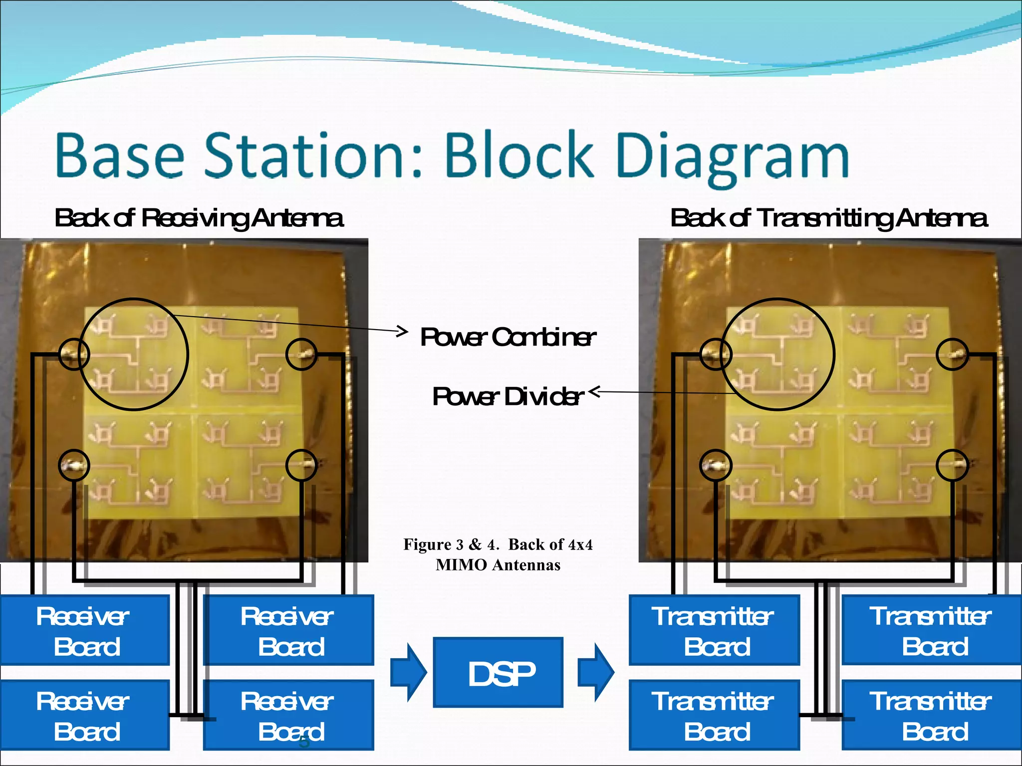
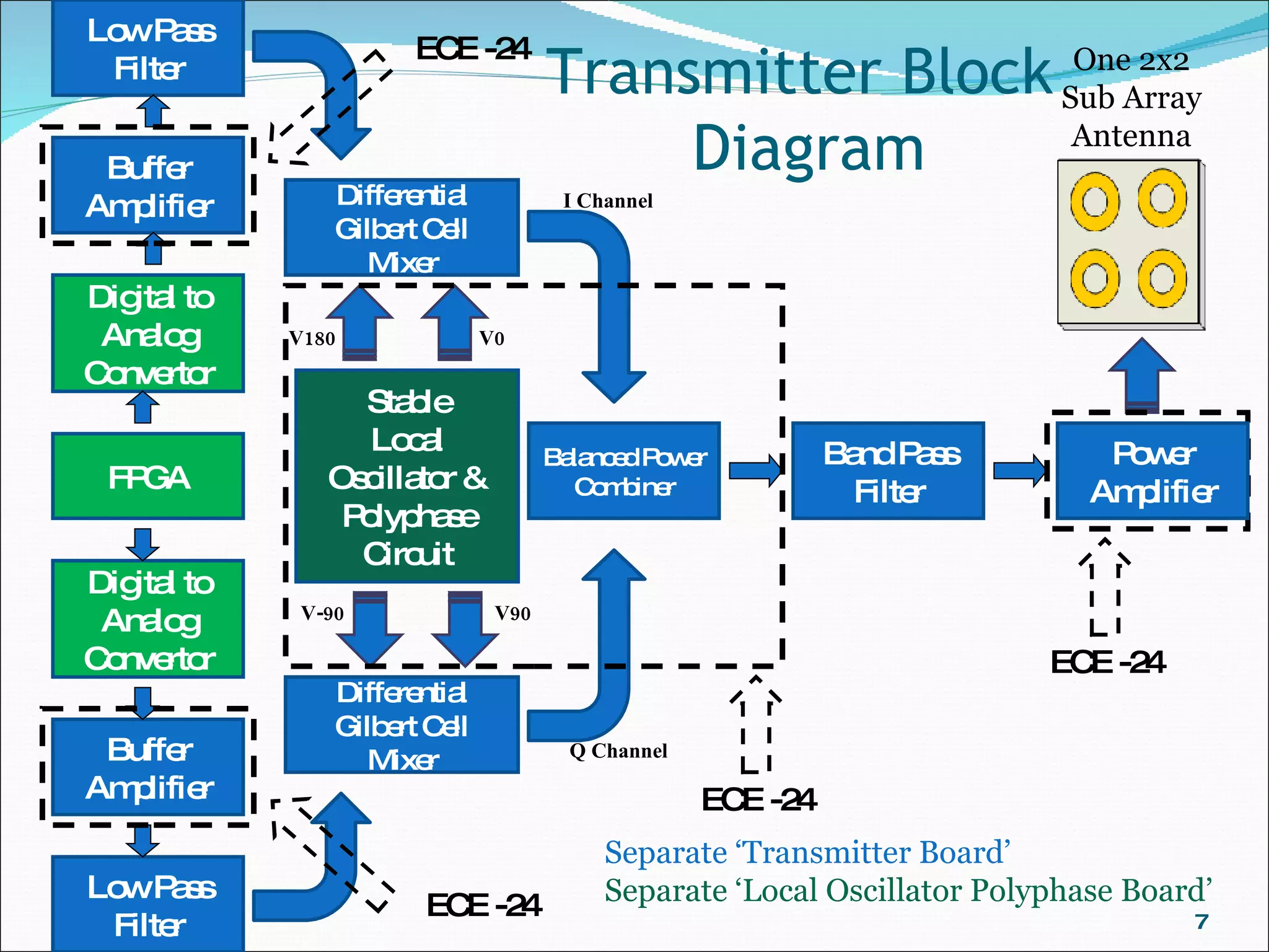
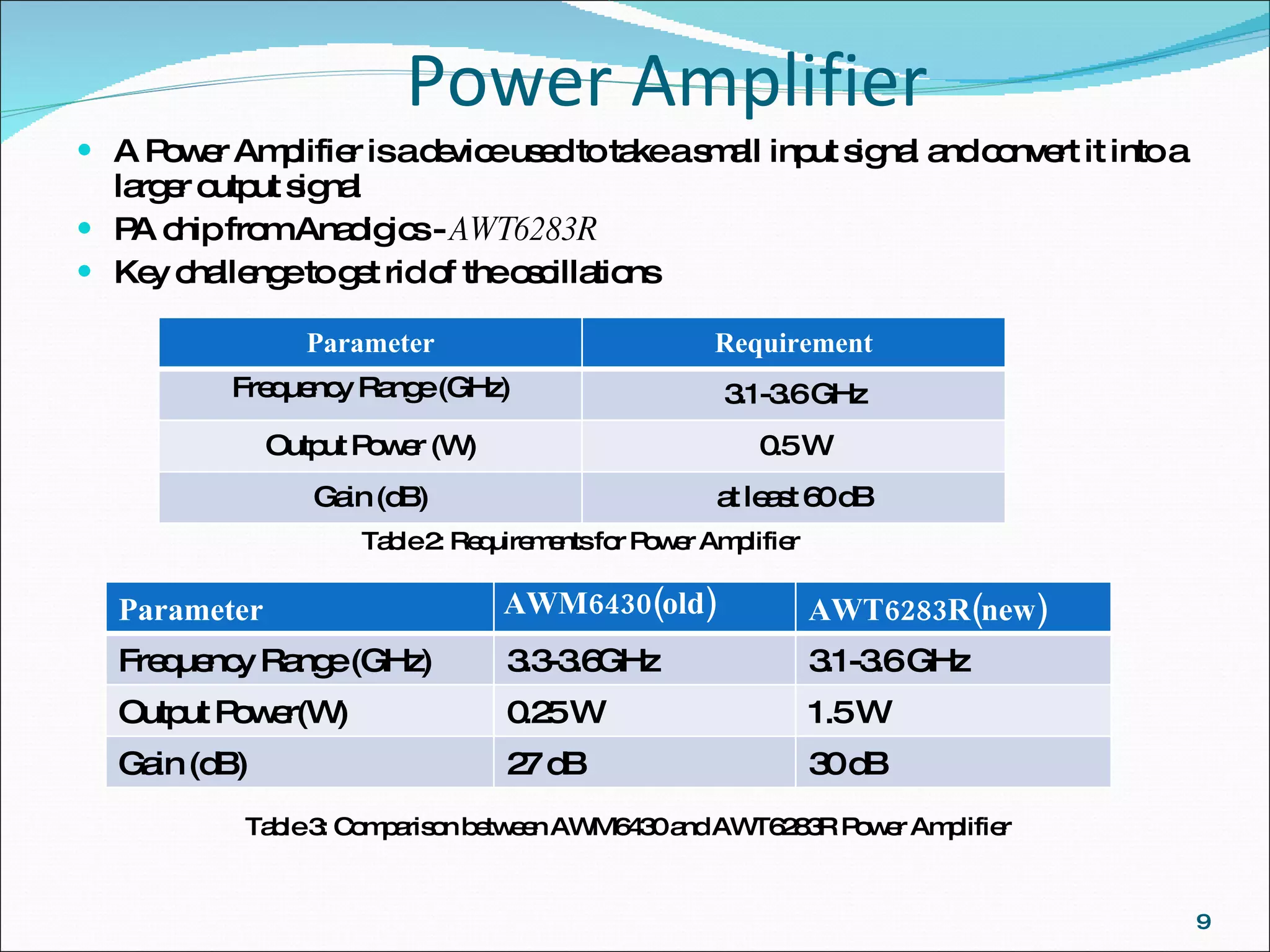
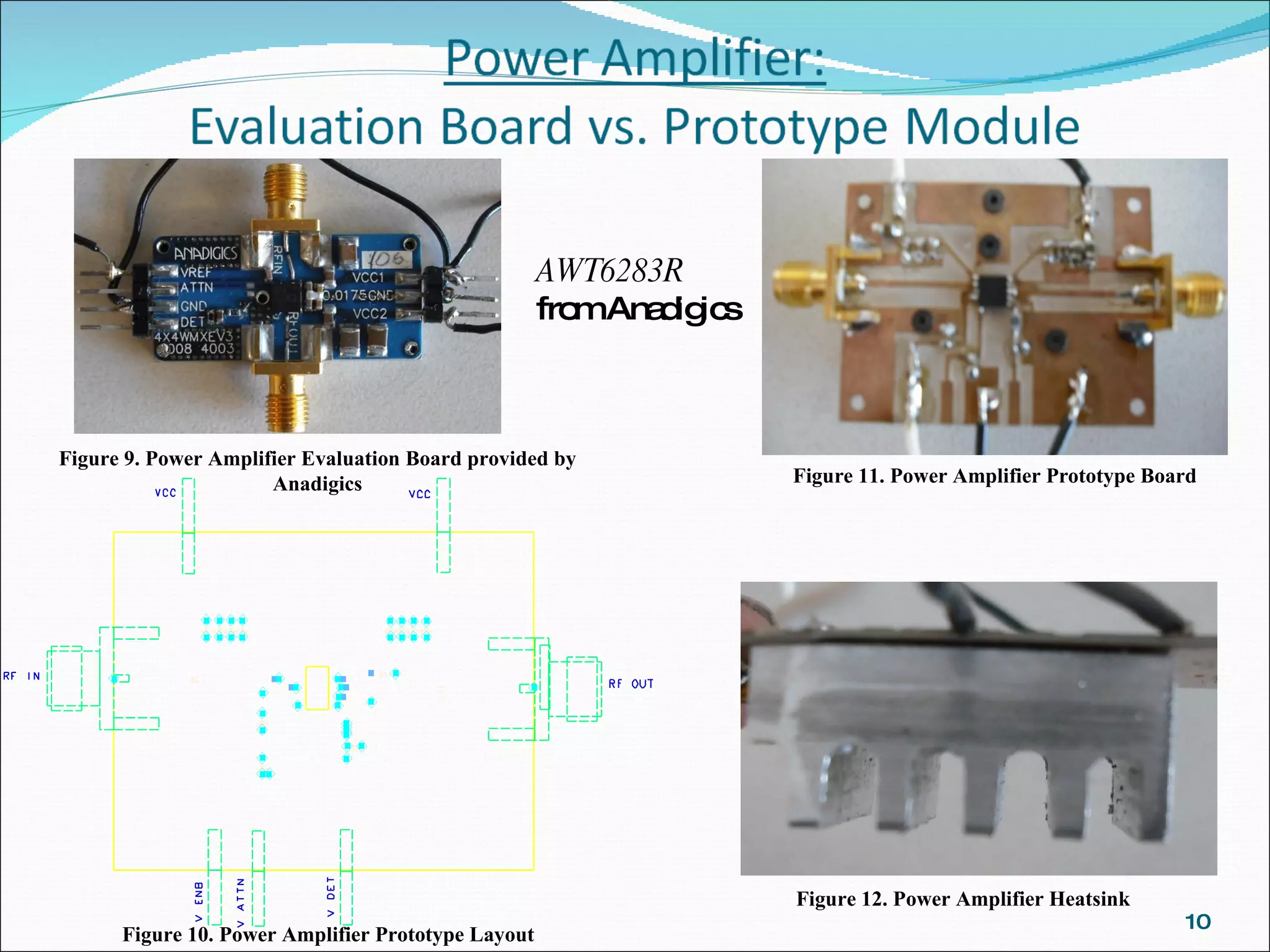
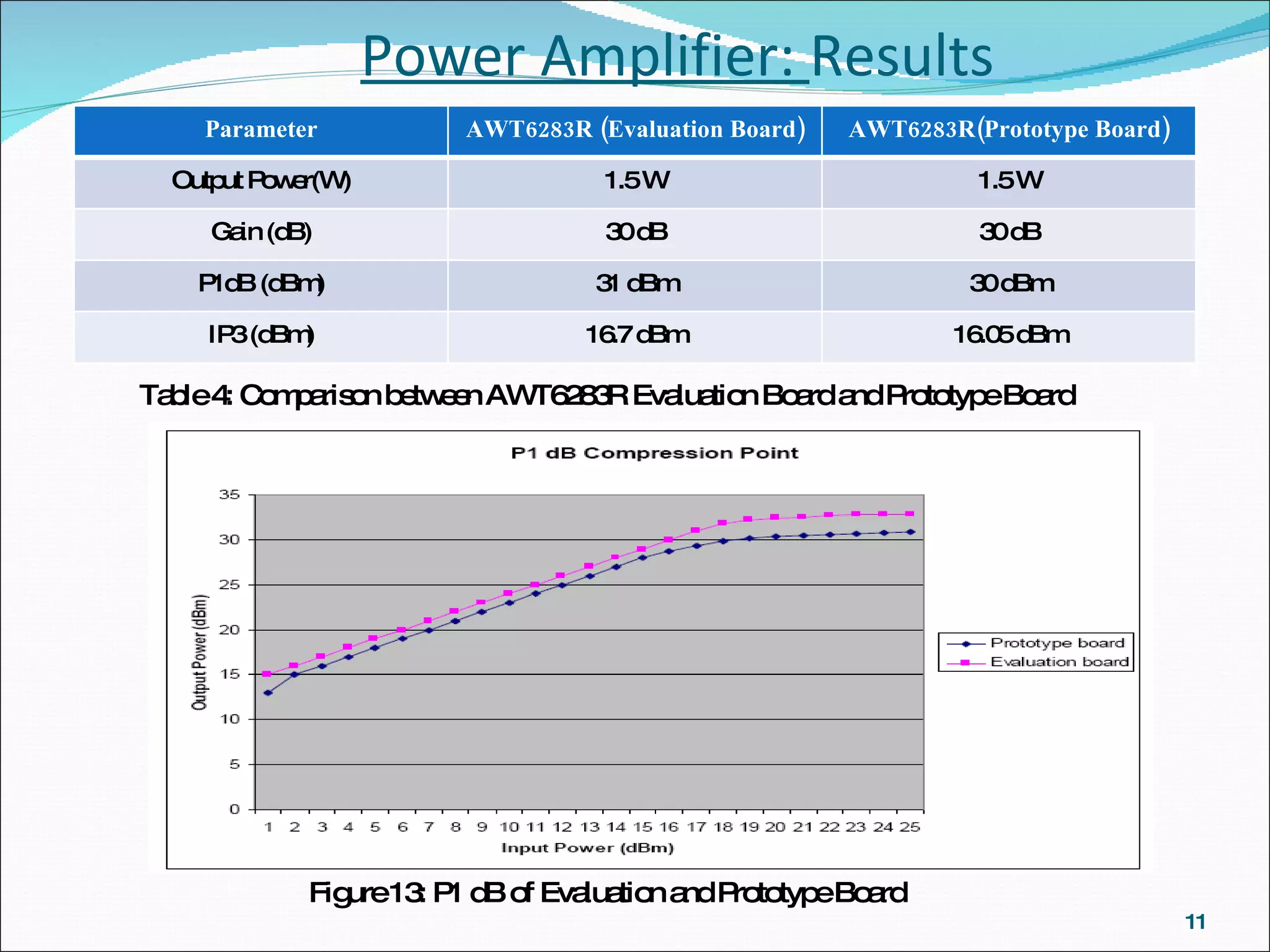
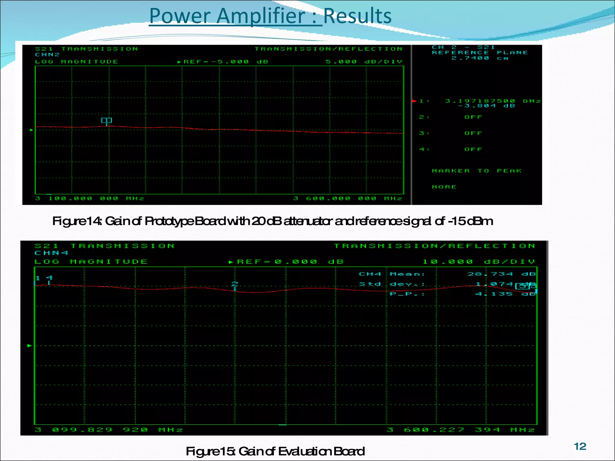
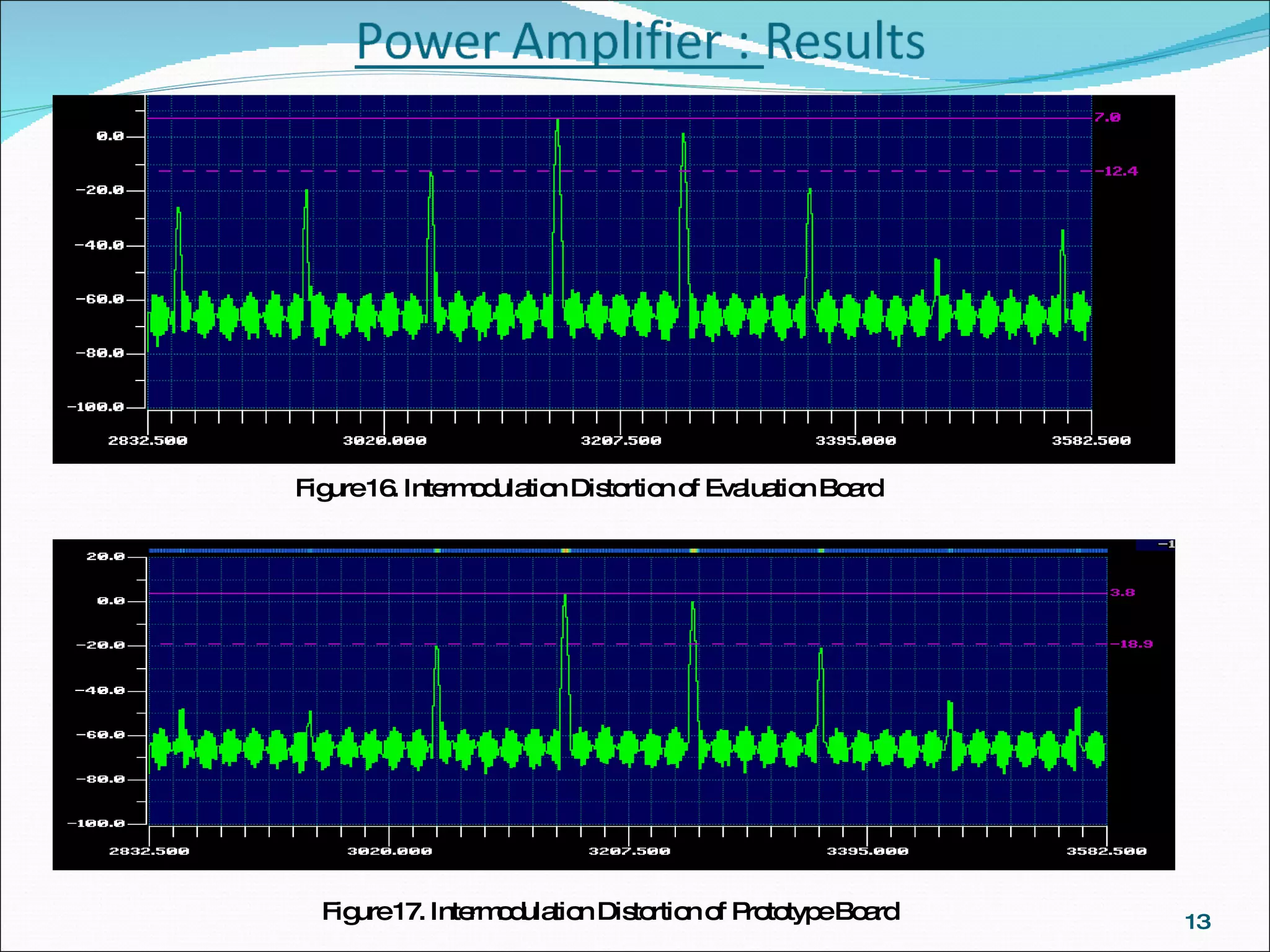
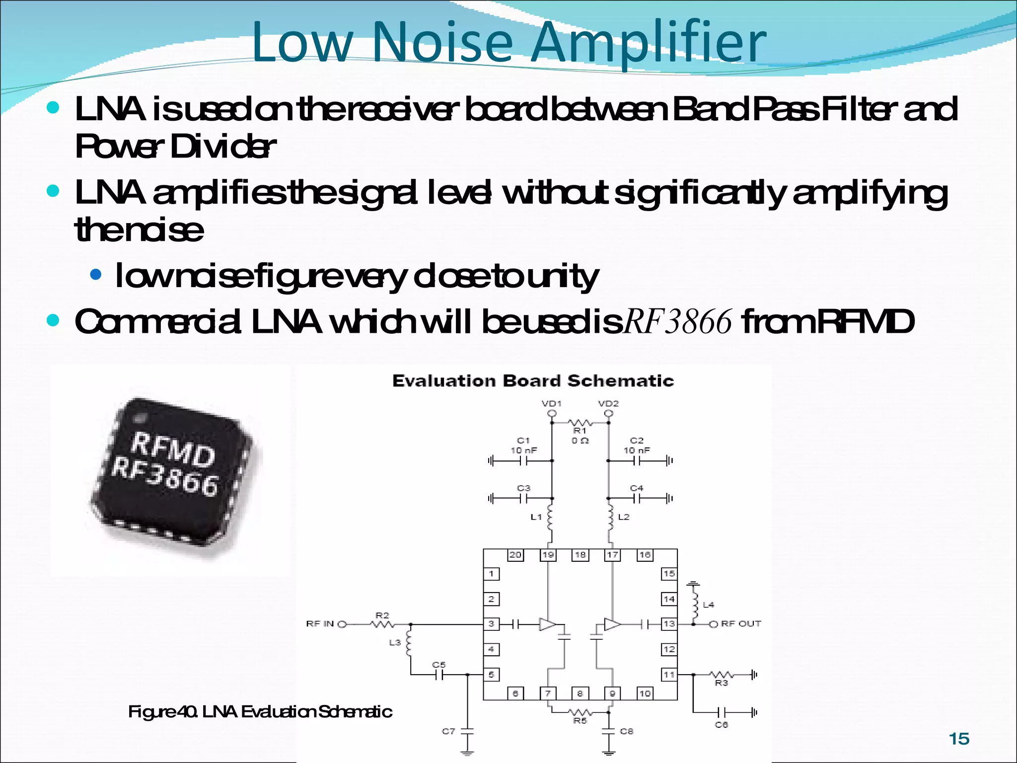
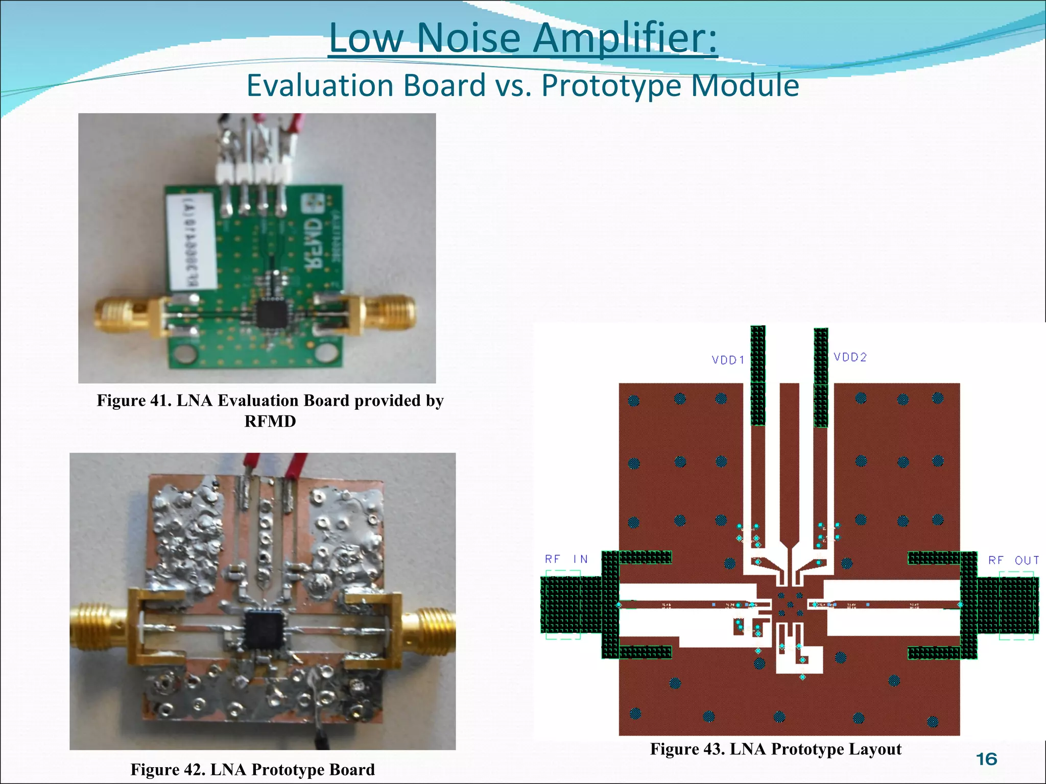
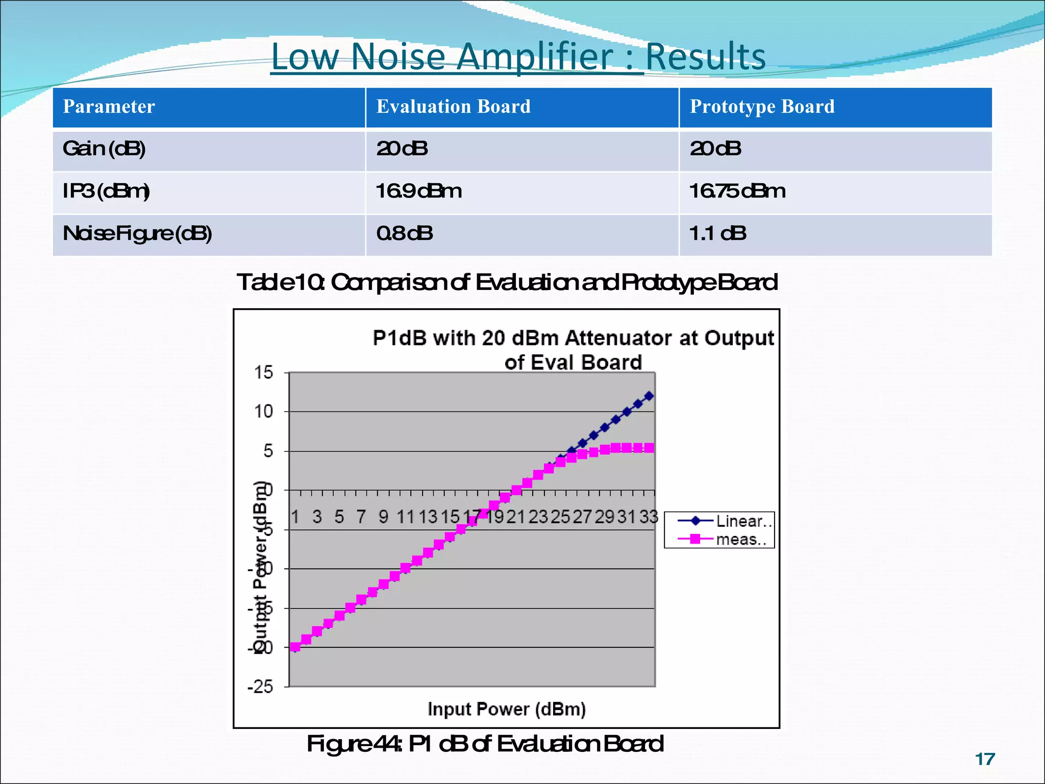
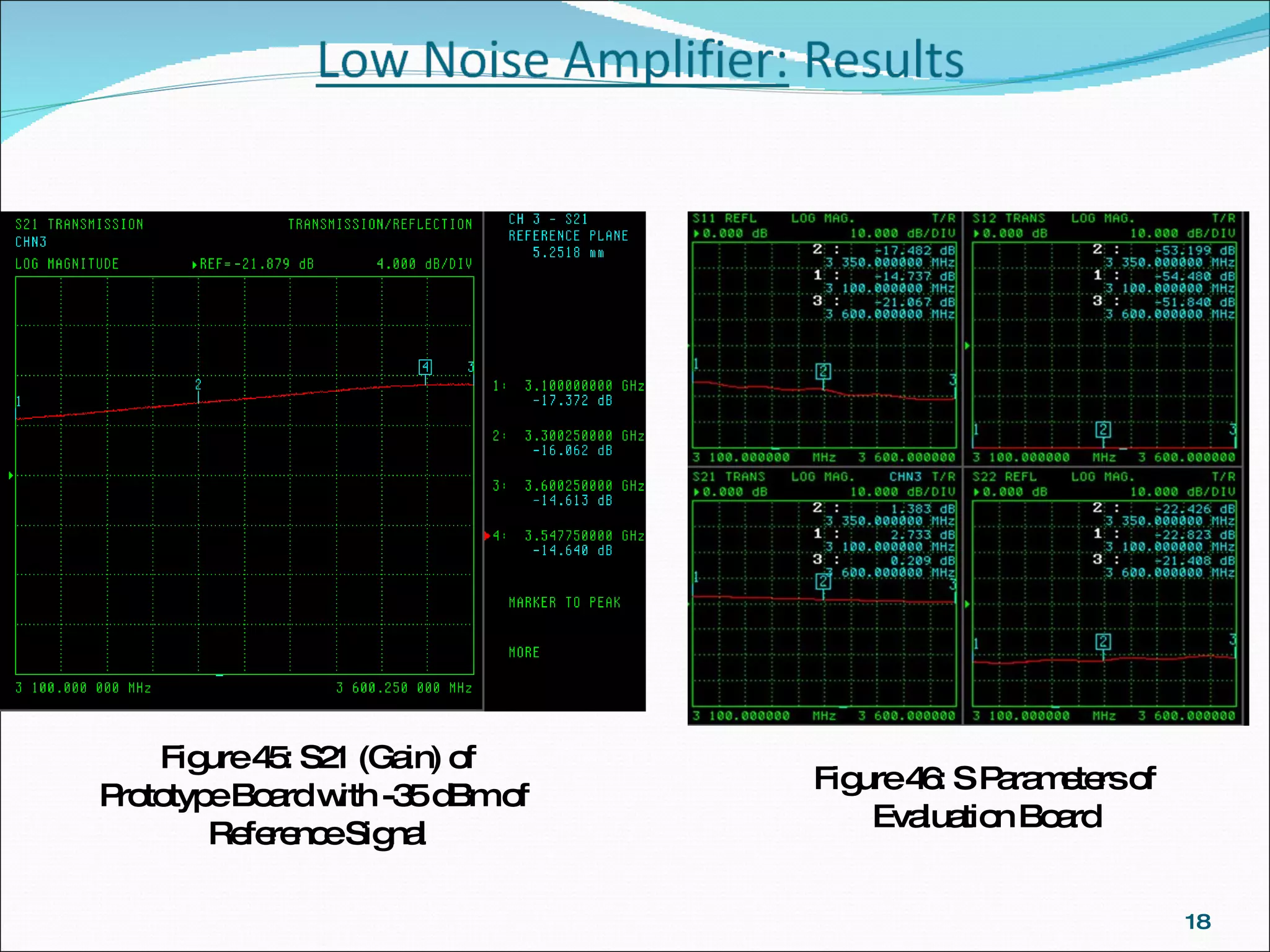
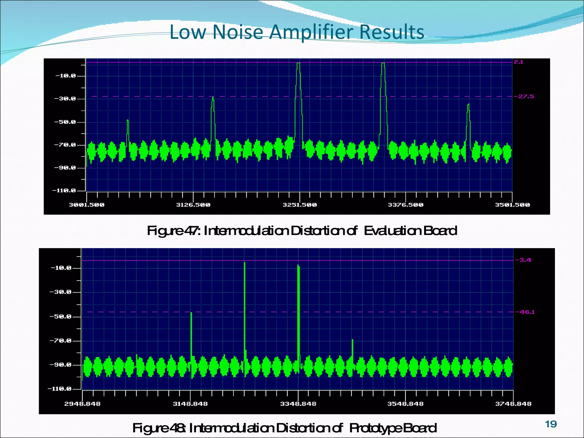
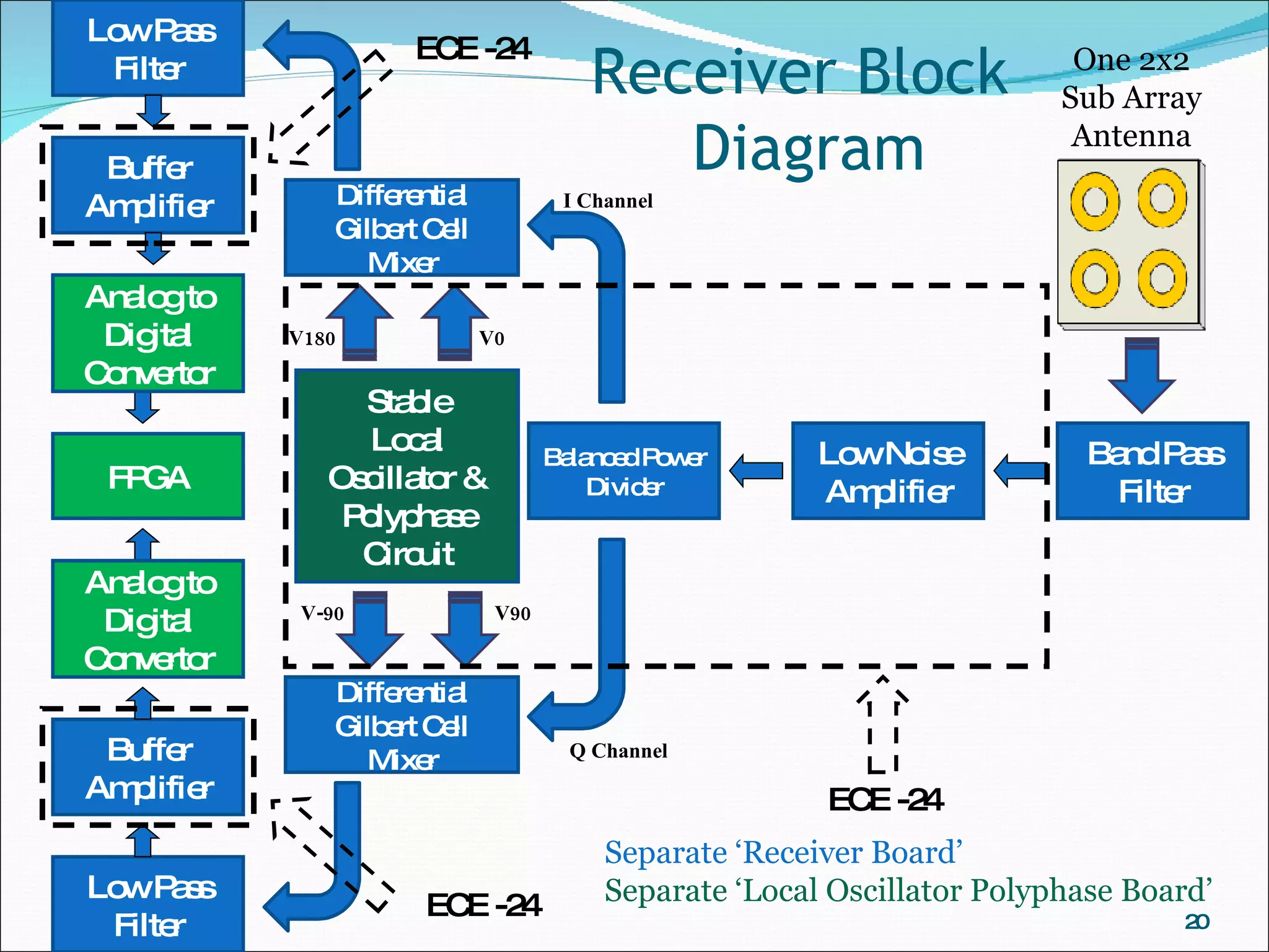
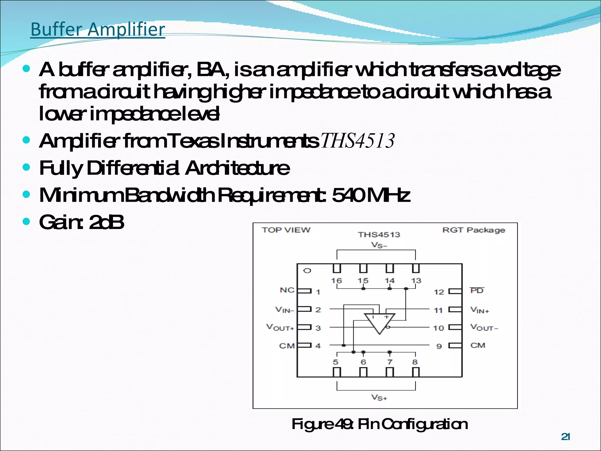
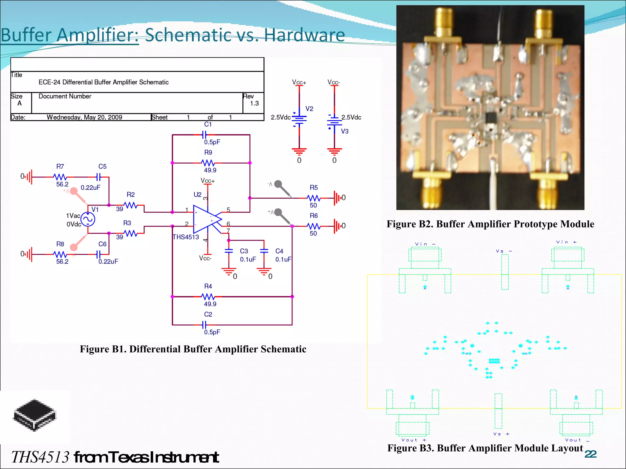
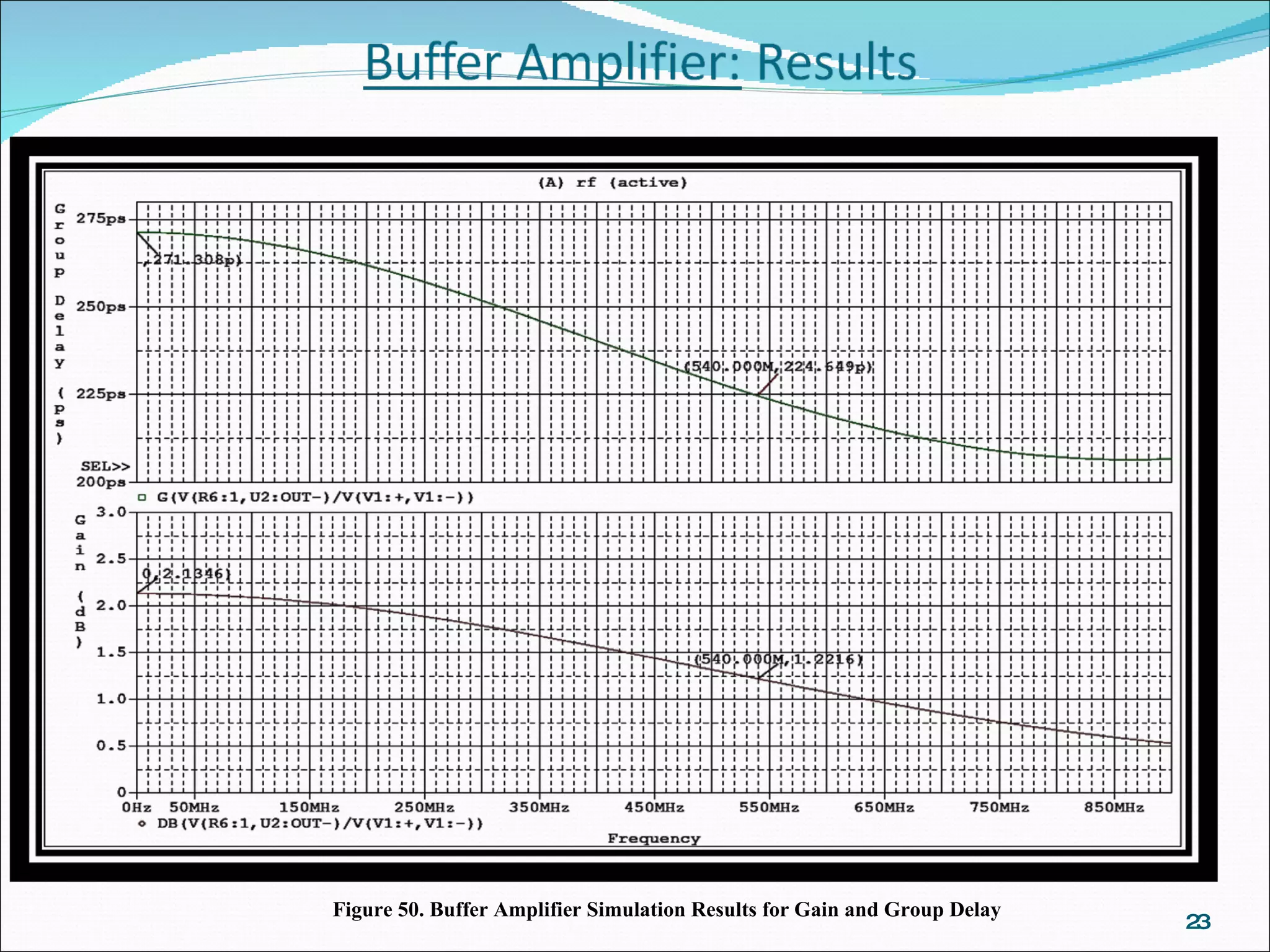
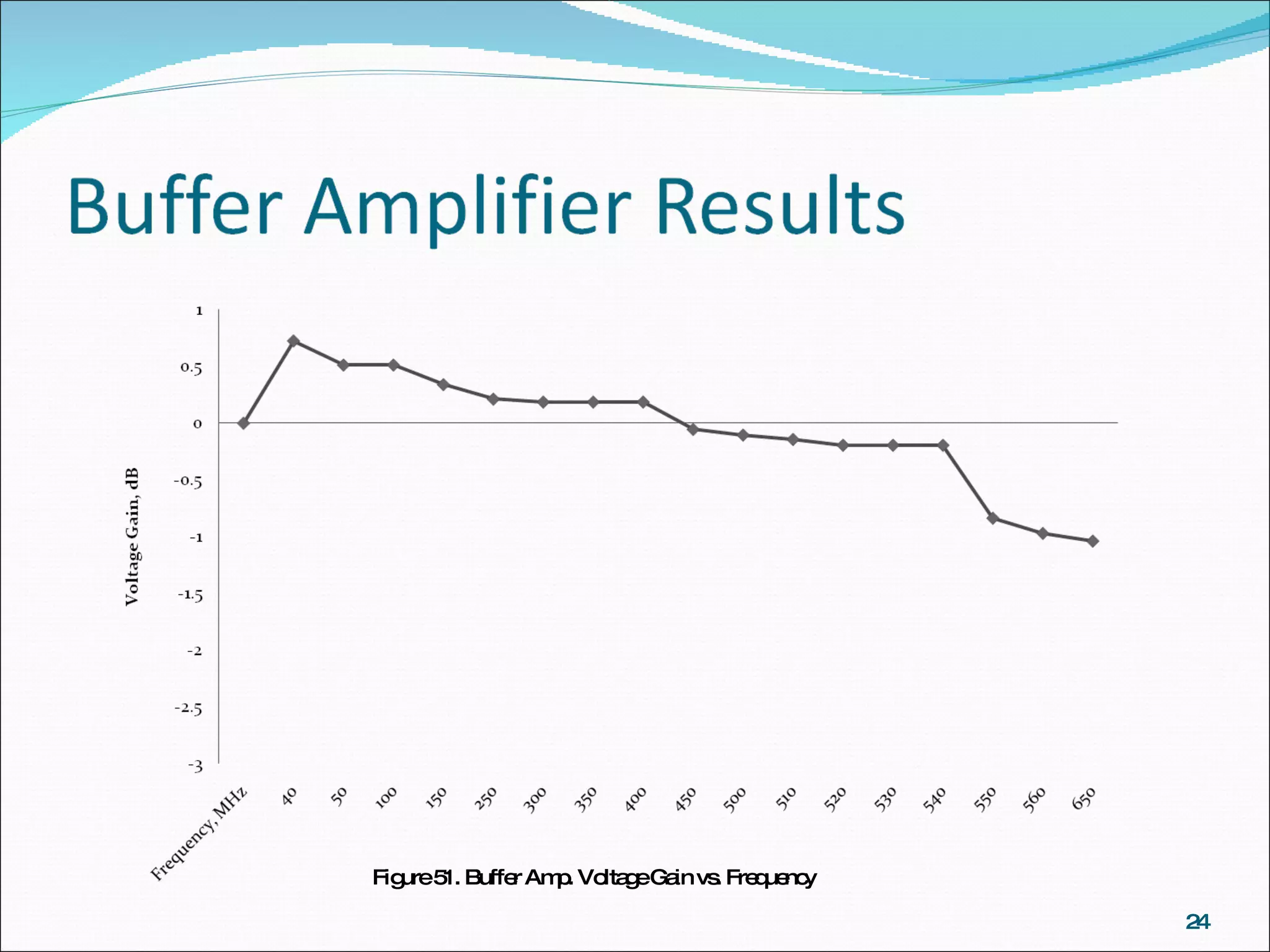
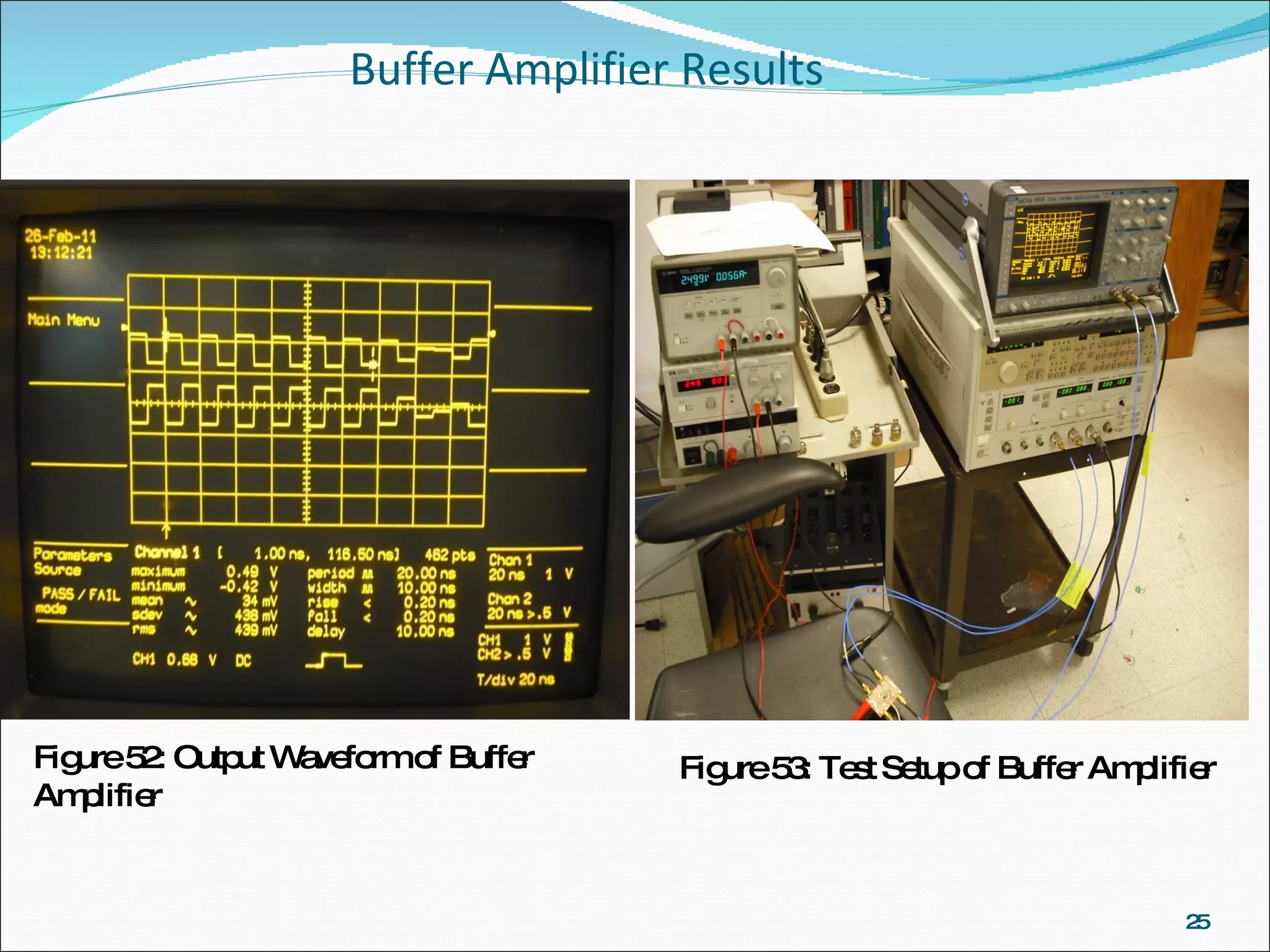
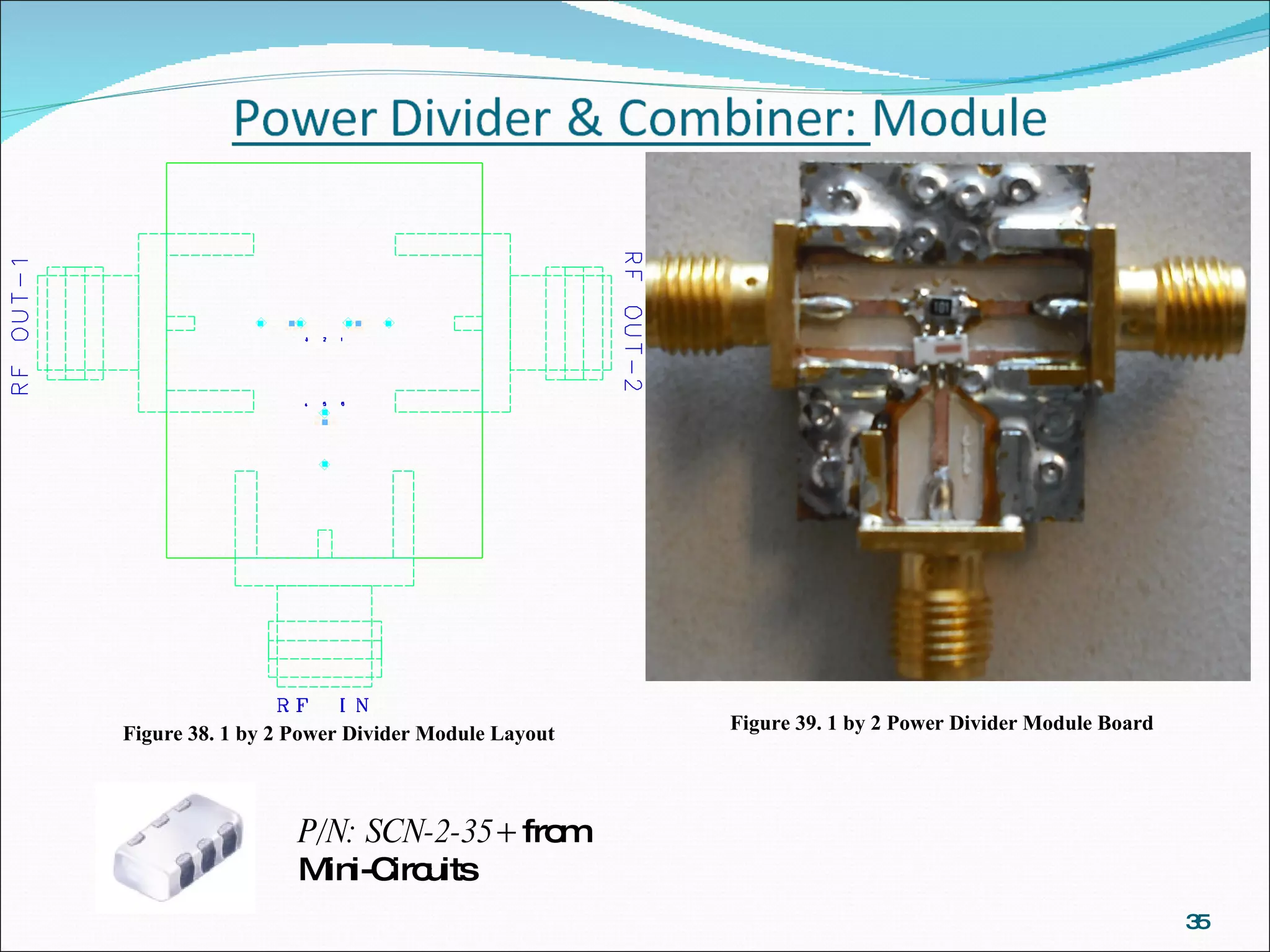
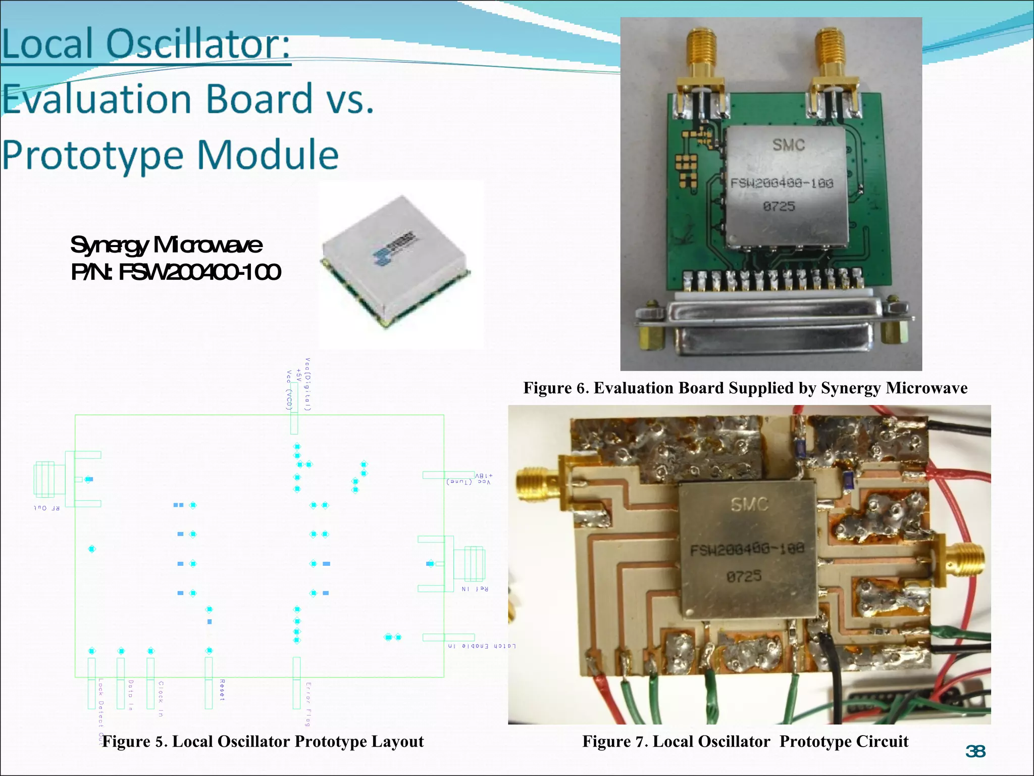
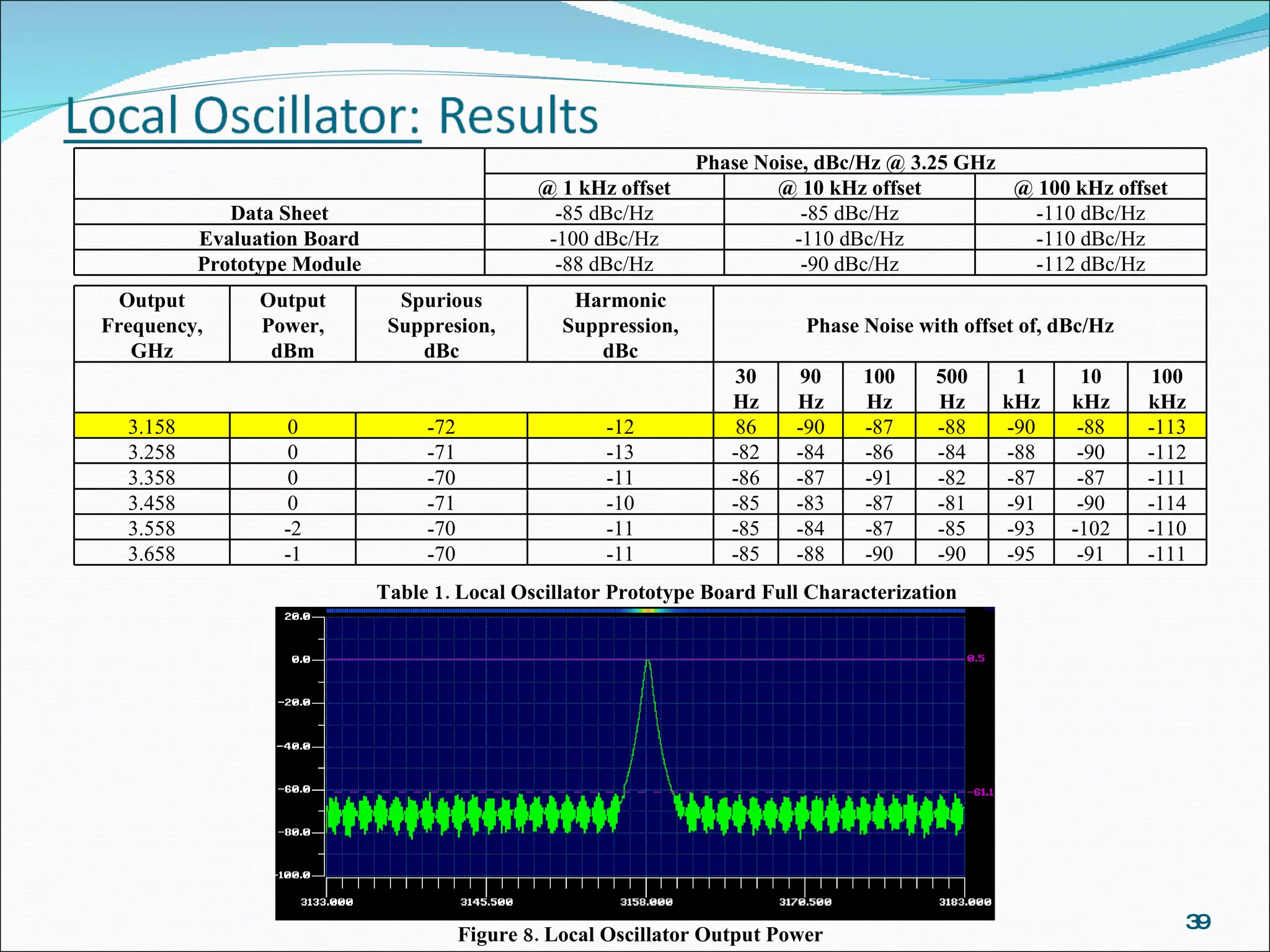
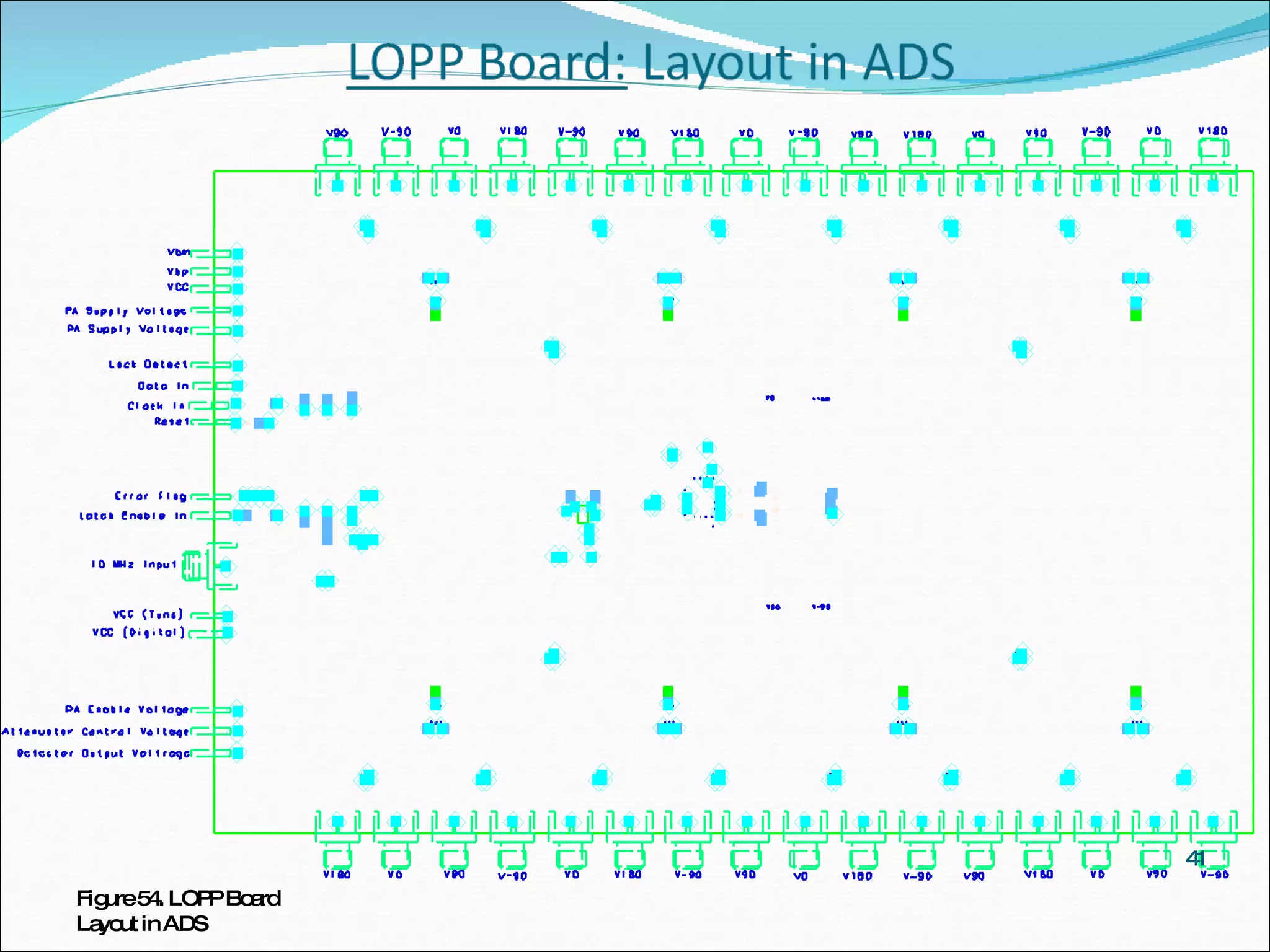
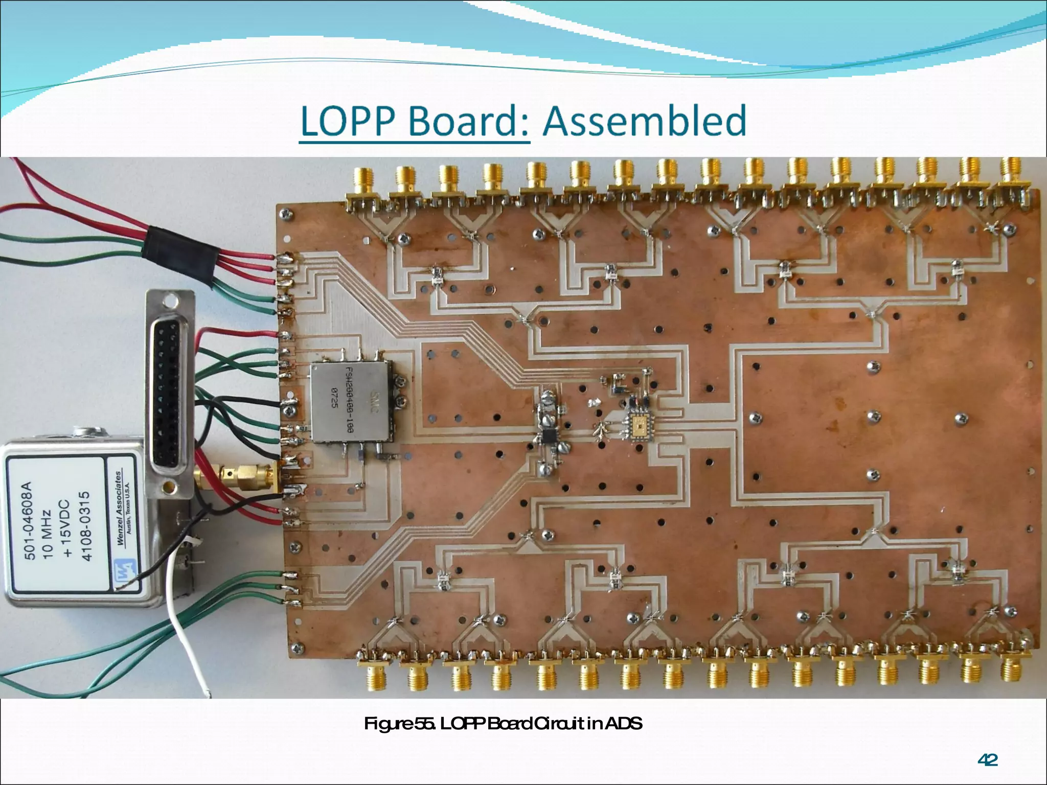
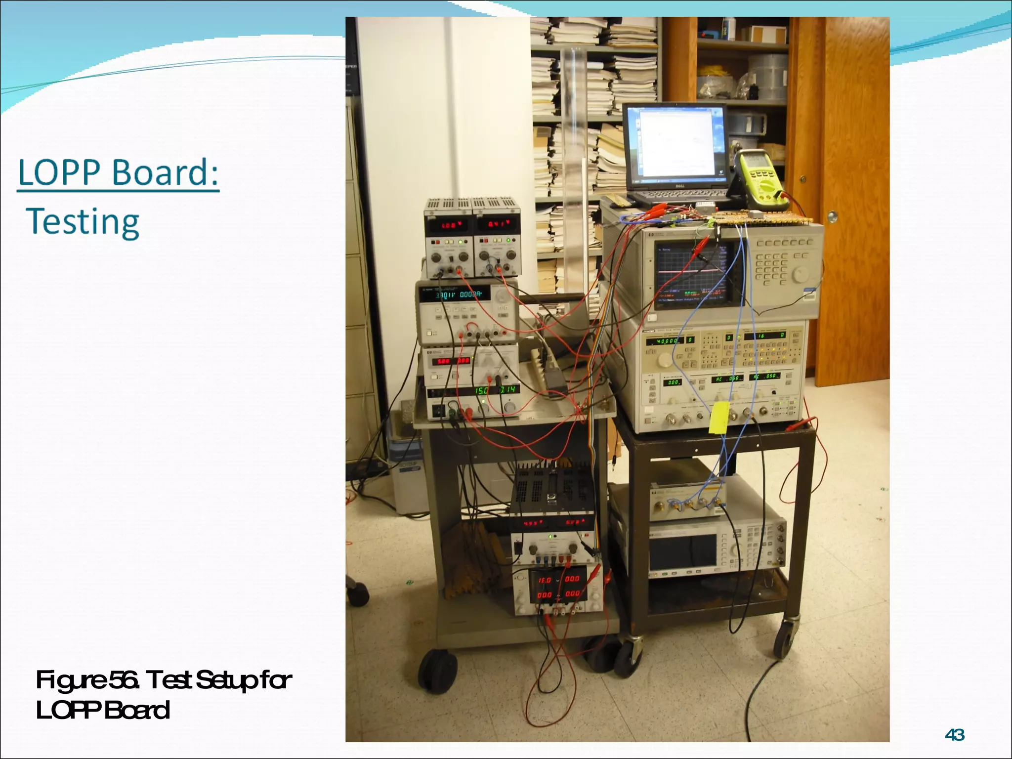
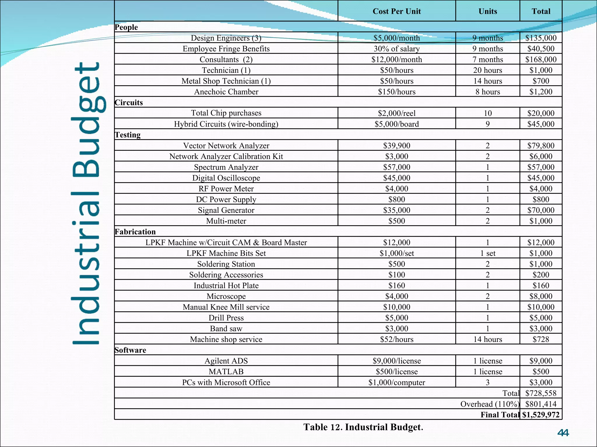
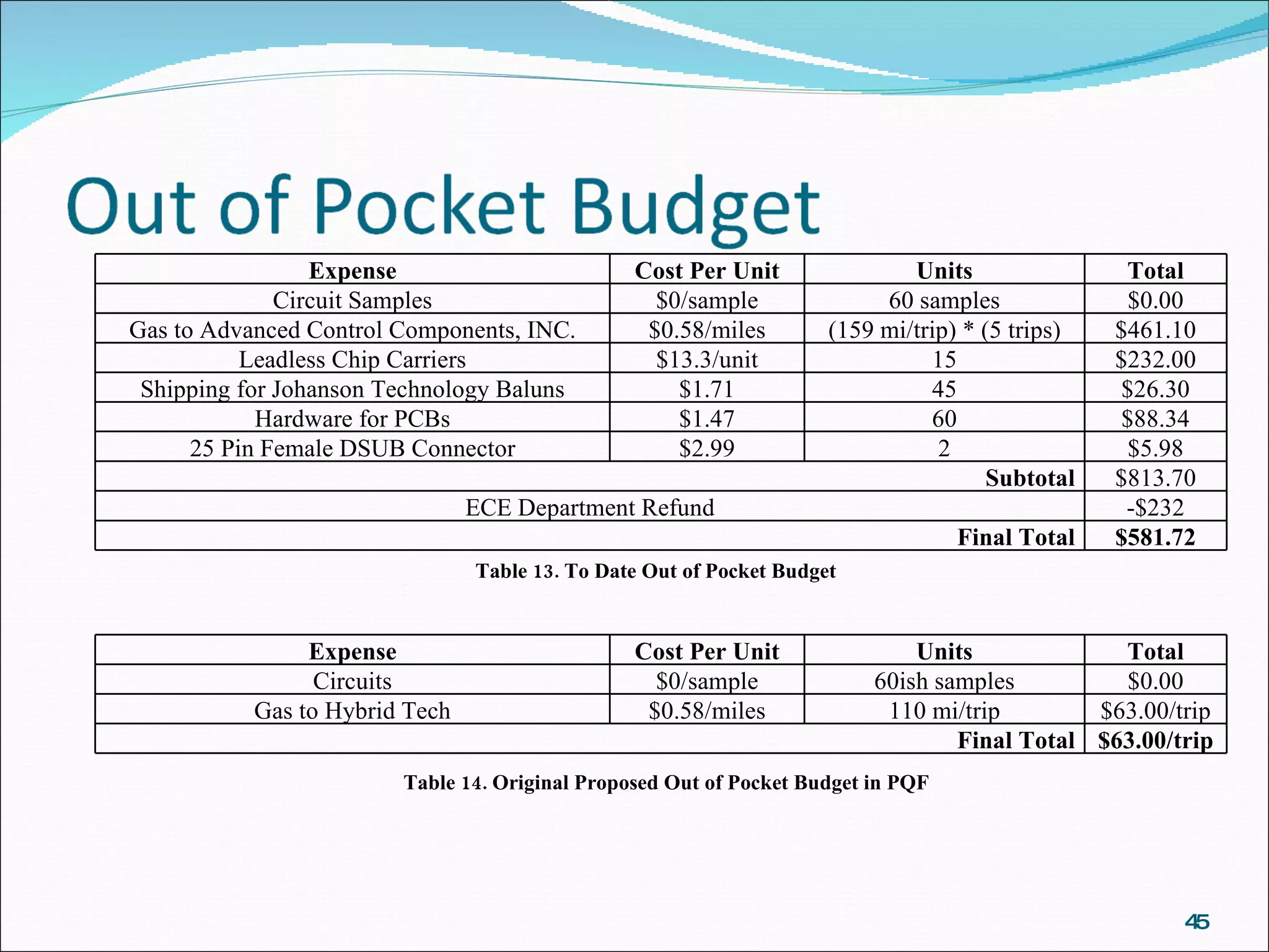
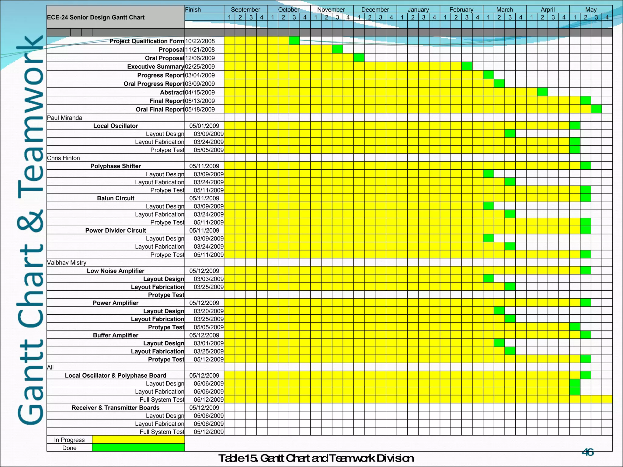
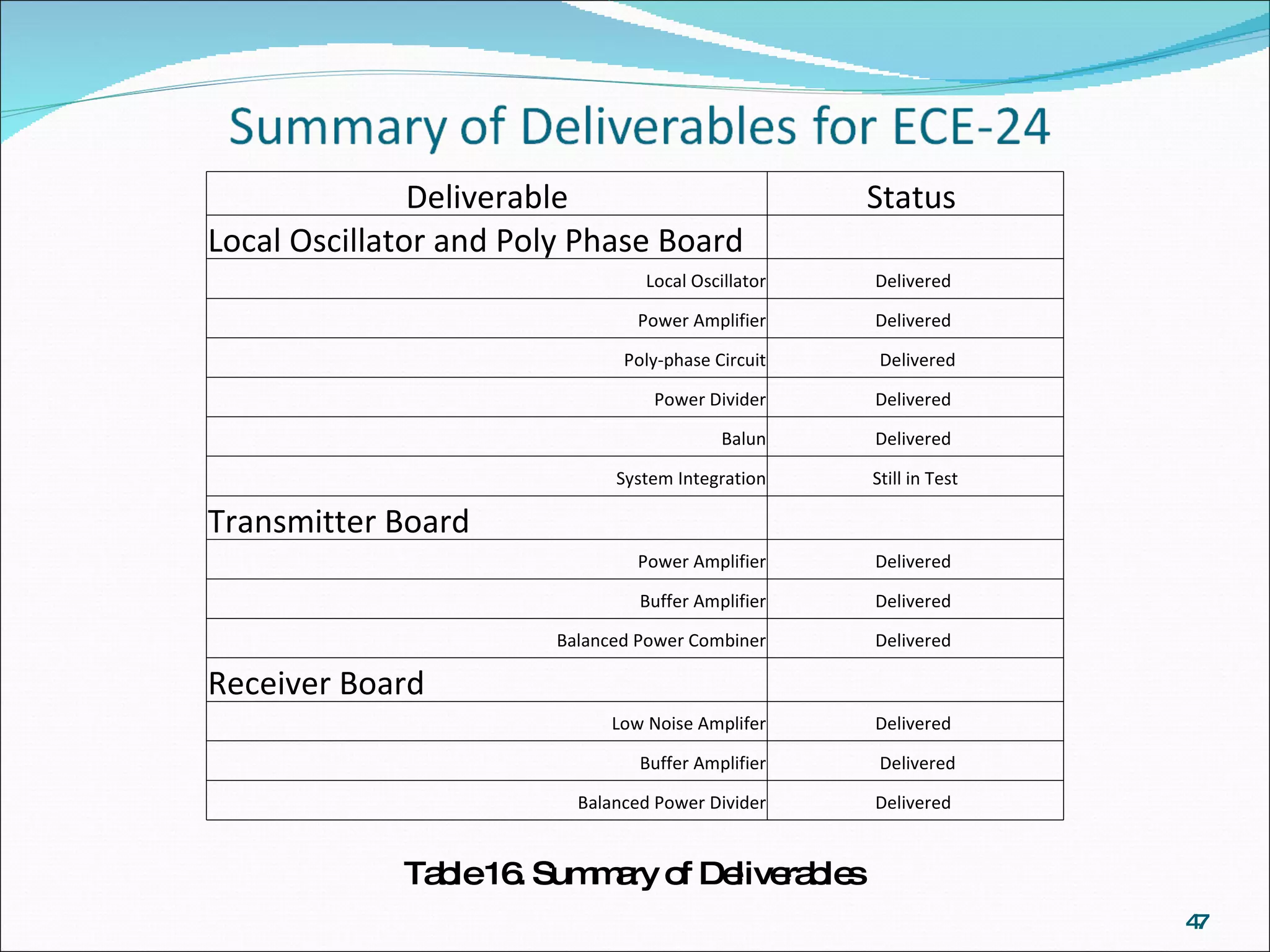
Members:  Chris Hinton Paul Miranda Vaibhav Mistry Team:  ECE-24 Advisor:  Dr. Daryoush
Outline of Presentation Problem description –What and Why? Solutions Base Station Overview Block Diagrams Digital Receiver Board LOPP Board Digital Transmitter Board Budget Schedule - Gantt Chart Summary of Deliverables Q/A Session
PROBLEM DESCRIPTION -  Progress to 4G? What is Ultra Wide Band? Ultra Wide Band was regulated by the FCC in 2002 to be dedicated for 4G telecommunication system in the frequency band of 3.1 to 10.6 GHz Our senior design team will be targeting the channel #1 of broadband OFDM (covering 3.168 to 3.696 GHz) Why is there a need for Ultra Wide Band in  Mobile networks ? The enormous bandwidth of the system meant that UWB could potentially offer data rates of the order of Gbps Very high data speeds ( Wireless USB, …) http://www.3gamericas.org/index.cfm?fuseaction=page&pageid=956 Figure 1. 3G Forecast
Receiving Antenna Transmitting Antenna DSP Receiver  Board Receiver  Board Receiver  Board Receiver  Board Transmitter  Board Transmitter  Board Transmitter  Board Transmitter  Board Figure 2 &3. 4x4 MIMO Antennas developed in 2002 under Dr. Daryoush
Power Combiner Power Divider Back of Receiving Antenna Back of Transmitting Antenna DSP Receiver  Board Receiver  Board Receiver  Board Receiver  Board Transmitter  Board Transmitter  Board Transmitter  Board Transmitter  Board Figure 3 & 4.  Back of 4x4 MIMO Antennas
Receiver Block  Diagram Band Pass Filter Balanced Power Divider Stable Local Oscillator & Polyphase Circuit Low Pass Filter Low Pass Filter I Channel Q Channel V180 V0 V-90 V90 ECE -24 Differential Gilbert Cell Mixer Differential Gilbert Cell Mixer One 2x2 Sub Array Antenna Low Noise Amplifier Buffer Amplifier Buffer Amplifier ECE -24 ECE -24 FPGA Analog to Digital Convertor Analog to Digital Convertor Separate ‘Receiver Board’ Separate ‘Local Oscillator Polyphase Board’
Transmitter Block  Diagram Balanced Power Combiner Stable Local Oscillator & Polyphase Circuit FPGA Digital to Analog Convertor Digital to Analog Convertor Low Pass Filter Low Pass Filter Separate ‘Transmitter Board’ Separate ‘Local Oscillator Polyphase Board’ I Channel Q Channel V180 V0 V-90 V90 ECE -24 Differential Gilbert Cell Mixer Differential Gilbert Cell Mixer One 2x2 Sub Array Antenna Band Pass Filter Buffer Amplifier Buffer Amplifier ECE -24 ECE -24 ECE -24 Power Amplifier
Power Amplifier A Power Amplifier is a device used to take a small input signal and convert it into a larger output signal PA chip from Anadigics -  AWT6283R Key challenge to get rid of the oscillations Table 2: Requirements for Power Amplifier Table 3: Comparison between AWM6430 and AWT6283R Power Amplifier Parameter Requirement Frequency Range (GHz) 3.1-3.6 GHz Output Power (W) 0.5 W Gain (dB) at least 60 dB Parameter AWM6430(old) AWT6283R(new) Frequency Range (GHz) 3.3-3.6GHz 3.1-3.6 GHz Output Power(W) 0.25 W 1.5 W Gain (dB) 27 dB 30 dB
AWT6283R   from Anadigics  Figure 9. Power Amplifier Evaluation Board provided by Anadigics Figure 11. Power Amplifier Prototype Board Figure 12. Power Amplifier Heatsink Figure 10. Power Amplifier Prototype Layout
Power Amplifier:  Results Table 4: Comparison between AWT6283R Evaluation Board and Prototype Board Figure 13: P1 dB of Evaluation and Prototype Board Parameter AWT6283R (Evaluation Board) AWT6283R(Prototype Board) Output Power(W) 1.5 W 1.5 W Gain (dB) 30 dB 30 dB P1dB (dBm) 31 dBm 30 dBm IP3 (dBm) 16.7 dBm 16.05 dBm
Power Amplifier :  Results Figure 14: Gain of Prototype Board with 20 dB attenuator and reference signal of -15 dBm Figure 15: Gain of Evaluation Board
Figure 17. Intermodulation Distortion of Prototype Board Figure 16. Intermodulation Distortion of Evaluation Board
Receiver Block  Diagram Band Pass Filter Balanced Power Divider Stable Local Oscillator & Polyphase Circuit Low Pass Filter Low Pass Filter I Channel Q Channel V180 V0 V-90 V90 ECE -24 Differential Gilbert Cell Mixer Differential Gilbert Cell Mixer One 2x2 Sub Array Antenna Low Noise Amplifier Buffer Amplifier Buffer Amplifier ECE -24 ECE -24 FPGA Analog to Digital Convertor Analog to Digital Convertor Separate ‘Receiver Board’ Separate ‘Local Oscillator Polyphase Board’
Low Noise Amplifier LNA is used on the receiver board between Band Pass Filter and Power Divider LNA amplifies the signal level without significantly amplifying the noise  low noise figure very close to unity Commercial LNA which will be used is  RF3866  from RFMD Figure 40. LNA Evaluation Schematic
Low Noise Amplifier: Evaluation Board vs. Prototype Module Figure 41. LNA Evaluation Board provided by RFMD Figure 42. LNA Prototype Board Figure 43. LNA Prototype Layout
Low Noise Amplifier :  Results Table 10: Comparison of Evaluation and Prototype Board Figure 44: P1 dB of Evaluation Board Parameter Evaluation Board Prototype Board Gain (dB) 20 dB 20 dB IP3 (dBm) 16.9 dBm 16.75 dBm Noise Figure (dB) 0.8 dB 1.1 dB
Figure 45: S21 (Gain) of Prototype Board with -35 dBm of  Reference Signal Figure 46: S Parameters of Evaluation Board
Low Noise Amplifier Results Figure 47: Intermodulation Distortion of  Evaluation Board Figure 48: Intermodulation Distortion of  Prototype Board
Receiver Block  Diagram Band Pass Filter Balanced Power Divider Stable Local Oscillator & Polyphase Circuit Low Pass Filter Low Pass Filter I Channel Q Channel V180 V0 V-90 V90 ECE -24 Differential Gilbert Cell Mixer Differential Gilbert Cell Mixer One 2x2 Sub Array Antenna Low Noise Amplifier Buffer Amplifier Buffer Amplifier ECE -24 ECE -24 FPGA Analog to Digital Convertor Analog to Digital Convertor Separate ‘Receiver Board’ Separate ‘Local Oscillator Polyphase Board’
Buffer Amplifier A buffer amplifier, BA, is an amplifier which transfers a voltage from a circuit having higher impedance to a circuit which has a lower impedance level Amplifier from Texas Instruments  THS4513 Fully Differential Architecture Minimum Bandwidth Requirement: 540 MHz Gain: 2dB Figure 49: Pin Configuration
THS4513  from Texas Instrument Figure B1. Differential Buffer Amplifier Schematic Figure B3. Buffer Amplifier Module Layout Figure B2. Buffer Amplifier Prototype Module
Figure 50. Buffer Amplifier Simulation Results for Gain and Group Delay
Figure 51. Buffer Amp. Voltage Gain vs. Frequency
Buffer Amplifier Results Figure 52: Output Waveform of Buffer Amplifier  Figure 53: Test Setup of Buffer Amplifier
Receiver Block  Diagram Band Pass Filter Balanced Power Divider Stable Local Oscillator & Polyphase Circuit Low Pass Filter Low Pass Filter I Channel Q Channel V180 V0 V-90 V90 ECE -24 Differential Gilbert Cell Mixer Differential Gilbert Cell Mixer One 2x2 Sub Array Antenna Low Noise Amplifier Buffer Amplifier Buffer Amplifier ECE -24 ECE -24 FPGA Analog to Digital Convertor Analog to Digital Convertor Separate ‘Receiver Board’ Separate ‘Local Oscillator Polyphase Board’
Local Oscillator  Polyphase Board Block Diagram Power Amplifier V0 V180 Differential  Polyphase  Shifter  V0 V90 V-90 V180 V0 Balun Balun V180 Balun Balun Balun V-90 V0 1:2 Extra 90° of T-Line Balun Balun Local Oscillator V90 V180 V-90 V90 1:2 Extra 90° of T-Line Balun Balun 1:2 Extra 90° of T-Line Balun Balun 1:2 Extra 90° of T-Line Balun Balun 1:2 Extra 90° of T-Line Balun Balun 1:2 Extra 90° of T-Line Balun Balun 1:2 Extra 90° of T-Line Balun Balun 1:2 Extra 90° of T-Line Balun Balun V90 V-90 V0 V180 V90 V-90 V0 V180 V-90 V90 V180 V0 V-90 V90 V180 V0 V180 V0 V90 V-90 V180 V0 V90 V-90 Vo V180 V-90 V90 Vo V180 V-90 V90
Figure 18. Broken Polyphase Alumina Board Figure 19. Polyphase IC developed under Dr. Daryoush in 2004 Figure 20. Polyphase IC epoxied on Leadless Chip Carrier
Figure 30. Polyphase Prototype Module Layout Figure 31. Polyphase Prototype Module Circuit
Figure 33. Polyphase Prototype Module Results Insertion Loss Magnitude (dB) & Phase (degree) Figure 32. Polyphase Prototype Module Testing Legend: V0 - yellow V90 - blue V180 - red V270 - black
Local Oscillator  Polyphase Board Block Diagram Power Amplifier V0 V180 Differential  Polyphase  Shifter  V0 V90 V-90 V180 V0 Balun Balun V180 Balun Balun Balun V-90 V0 1:2 Extra 90° of T-Line Balun Balun Local Oscillator V90 V180 V-90 V90 1:2 Extra 90° of T-Line Balun Balun 1:2 Extra 90° of T-Line Balun Balun 1:2 Extra 90° of T-Line Balun Balun 1:2 Extra 90° of T-Line Balun Balun 1:2 Extra 90° of T-Line Balun Balun 1:2 Extra 90° of T-Line Balun Balun 1:2 Extra 90° of T-Line Balun Balun V90 V-90 V0 V180 V90 V-90 V0 V180 V-90 V90 V180 V0 V-90 V90 V180 V0 V180 V0 V90 V-90 V180 V0 V90 V-90 Vo V180 V-90 V90 Vo V180 V-90 V90
Figure 34.  Balun Module Layout Figure 35. Balun Module Board P/N 3600BL14M100  from Johanson Technology
Table 7. Balun Data Sheet Table 8. Balun Prototype Data Figure 36 and 37. Insertion Loss and Phase Difference Respectively Balun             Frequency (GHz) 3.158 3.258 3.358 3.458 3.558 3.658 Insertion Loss (dB)             J1-J2 3.4 3.7 4.2 4.3 4.7 4.5 J1-J3 3.4 3.3 3.2 3.2 3.1 3.3 Return Loss (dB)             J1-J2 12.9 14.5 17.2 19.1 18.2 17.6 J1-J3 13.8 15.3 21.3 22.1 23.6 20.5 Phase Change(deg)             J1-J2 (ref)             J1-J3 171.4 171.9 172.7 177.4 178.4 179.8 Frequency (MHz) 3300~3900 Unbalanced Impedence 50 Ω Differential Balanced Impedance 100 Ω Insertion Loss 1.2 dB Max Return Loss 9.5 dB min Phase Difference 180° ± 15 Amplitude Difference 1.5 dB max.
Local Oscillator  Polyphase Board Block Diagram Power Amplifier V0 V180 Differential  Polyphase  Shifter  V0 V90 V-90 V180 V0 Balun Balun V180 Balun Balun Balun V-90 V0 1:2 Extra 90° of T-Line Balun Balun Local Oscillator V90 V180 V-90 V90 1:2 Extra 90° of T-Line Balun Balun 1:2 Extra 90° of T-Line Balun Balun 1:2 Extra 90° of T-Line Balun Balun 1:2 Extra 90° of T-Line Balun Balun 1:2 Extra 90° of T-Line Balun Balun 1:2 Extra 90° of T-Line Balun Balun 1:2 Extra 90° of T-Line Balun Balun V90 V-90 V0 V180 V90 V-90 V0 V180 V-90 V90 V180 V0 V-90 V90 V180 V0 V180 V0 V90 V-90 V180 V0 V90 V-90 Vo V180 V-90 V90 Vo V180 V-90 V90
Figure 38. 1 by 2 Power Divider Module Layout Figure 39. 1 by 2 Power Divider Module Board P/N: SCN-2-35+  from Mini-Circuits
Table 8. Power Divider Prototype Data Results Table 9. Power Divider Datasheet  Figure 39. Power Divider Insertion Loss in dB Power Divider             Frequency (GHz) 3.158 3.258 3.358 3.458 3.558 3.658 Insertion Loss (dB)             J1-J2 3.4 3.4 3.4 3.4 3.4 3.4 J1-J3 3.4 3.4 3.4 3.4 3.4 3.4 Return Loss (dB)             J1-J2 15.3 14.9 14.1 13.7 13.2 12.8 J1-J3 15.3 14.9 14.1 13.7 13.2 12.8 Phase Change(deg)             J1-J2 (ref)             J1-J3 1.4 1.5 1.4 1.3 1.4 1.4 Frequency (MHz) 3100 3200 3300 3450 3500 3550 3575 3600 3625 3650 Insertion Loss (dB)                     J1-J2 3.51 3.5 3.5 3.54 3.57 3.6 3.62 3.63 3.65 3.66 J1-J3 3.46 3.45 3.46 3.51 3.53 3.55 3.57 3.58 3.6 3.62 Amplitude Unbalance (dB) 0.05 0.05 0.04 0.04 0.04 0.04 0.05 0.05 0.05 0.05 Isolation (dB) 18.47 20.26 22.71 27.85 29.97 31.81 32.2 32.06 31.43 30.5 Return Loss (dB) 21.86 26.24 30.1 21.98 20.75 19.7 19.31 18.95 18.61 18.26
Local Oscillator  Polyphase Board Block Diagram Power Amplifier V0 V180 Differential  Polyphase  Shifter  V0 V90 V-90 V180 V0 Balun Balun V180 Balun Balun Balun V-90 V0 1:2 Extra 90° of T-Line Balun Balun Local Oscillator V90 V180 V-90 V90 1:2 Extra 90° of T-Line Balun Balun 1:2 Extra 90° of T-Line Balun Balun 1:2 Extra 90° of T-Line Balun Balun 1:2 Extra 90° of T-Line Balun Balun 1:2 Extra 90° of T-Line Balun Balun 1:2 Extra 90° of T-Line Balun Balun 1:2 Extra 90° of T-Line Balun Balun V90 V-90 V0 V180 V90 V-90 V0 V180 V-90 V90 V180 V0 V-90 V90 V180 V0 V180 V0 V90 V-90 V180 V0 V90 V-90 Vo V180 V-90 V90 Vo V180 V-90 V90
Figure 5. Local Oscillator Prototype Layout Figure 7. Local Oscillator  Prototype Circuit Figure 6. Evaluation Board Supplied by Synergy Microwave Synergy Microwave P/N: FSW200400-100
Table 1. Local Oscillator Prototype Board Full Characterization Figure 8. Local Oscillator Output Power Phase Noise, dBc/Hz @ 3.25 GHz @ 1 kHz offset @ 10 kHz offset @ 100 kHz offset Data Sheet -85 dBc/Hz -85 dBc/Hz -110 dBc/Hz Evaluation Board -100 dBc/Hz -110 dBc/Hz -110 dBc/Hz Prototype Module -88 dBc/Hz -90 dBc/Hz -112 dBc/Hz Output Frequency, GHz Output Power, dBm Spurious Suppresion, dBc Harmonic Suppression, dBc Phase Noise with offset of, dBc/Hz 30 Hz 90 Hz 100 Hz 500 Hz 1 kHz 10 kHz 100 kHz 3.158 0 -72 -12 86 -90 -87 -88 -90 -88 -113 3.258 0 -71 -13 -82 -84 -86 -84 -88 -90 -112 3.358 0 -70 -11 -86 -87 -91 -82 -87 -87 -111 3.458 0 -71 -10 -85 -83 -87 -81 -91 -90 -114 3.558 -2 -70 -11 -85 -84 -87 -85 -93 -102 -110 3.658 -1 -70 -11 -85 -88 -90 -90 -95 -91 -111
Local Oscillator  Polyphase Board Block Diagram Power Amplifier V0 V180 Differential  Polyphase  Shifter  V0 V90 V-90 V180 V0 Balun Balun V180 Balun Balun Balun V-90 V0 1:2 Extra 90° of T-Line Balun Balun Local Oscillator V90 V180 V-90 V90 1:2 Extra 90° of T-Line Balun Balun 1:2 Extra 90° of T-Line Balun Balun 1:2 Extra 90° of T-Line Balun Balun 1:2 Extra 90° of T-Line Balun Balun 1:2 Extra 90° of T-Line Balun Balun 1:2 Extra 90° of T-Line Balun Balun 1:2 Extra 90° of T-Line Balun Balun V90 V-90 V0 V180 V90 V-90 V0 V180 V-90 V90 V180 V0 V-90 V90 V180 V0 V180 V0 V90 V-90 V180 V0 V90 V-90 Vo V180 V-90 V90 Vo V180 V-90 V90
Figure 54. LOPP Board Layout in ADS
Figure 55. LOPP Board Circuit in ADS
Figure 56. Test Setup for LOPP Board
Table 12. Industrial Budget. Cost Per Unit Units Total People Design Engineers (3) $5,000/month 9 months $135,000 Employee Fringe Benefits 30% of salary 9 months $40,500 Consultants  (2) $12,000/month 7 months $168,000 Technician (1) $50/hours 20 hours $1,000 Metal Shop Technician (1) $50/hours 14 hours $700 Anechoic Chamber $150/hours 8 hours $1,200 Circuits Total Chip purchases $2,000/reel 10 $20,000 Hybrid Circuits (wire-bonding) $5,000/board 9 $45,000 Testing Vector Network Analyzer $39,900 2 $79,800 Network Analyzer Calibration Kit $3,000 2 $6,000 Spectrum Analyzer $57,000 1 $57,000 Digital Oscilloscope $45,000 1 $45,000 RF Power Meter $4,000 1 $4,000 DC Power Supply $800 1 $800 Signal Generator $35,000 2 $70,000 Multi-meter $500 2 $1,000 Fabrication LPKF Machine w/Circuit CAM & Board Master $12,000 1 $12,000 LPKF Machine Bits Set $1,000/set 1 set $1,000 Soldering Station $500 2 $1,000 Soldering Accessories $100 2 $200 Industrial Hot Plate $160 1 $160 Microscope $4,000 2 $8,000 Manual Knee Mill service $10,000 1 $10,000 Drill Press $5,000 1 $5,000 Band saw $3,000 1 $3,000 Machine shop service $52/hours 14 hours $728 Software Agilent ADS $9,000/license 1 license $9,000 MATLAB $500/license 1 license $500 PCs with Microsoft Office $1,000/computer 3 $3,000 Total $728,558 Overhead (110%) $801,414 Final Total $1,529,972
Table 13. To Date Out of Pocket Budget Table 14. Original Proposed Out of Pocket Budget in PQF Expense Cost Per Unit Units Total Circuit Samples $0/sample 60 samples $0.00 Gas to Advanced Control Components, INC. $0.58/miles (159 mi/trip) * (5 trips) $461.10 Leadless Chip Carriers $13.3/unit 15 $232.00 Shipping for Johanson Technology Baluns $1.71 45 $26.30 Hardware for PCBs $1.47 60 $88.34 25 Pin Female DSUB Connector $2.99 2 $5.98 Subtotal $813.70 ECE Department Refund -$232 Final Total $581.72 Expense Cost Per Unit Units Total Circuits $0/sample 60ish samples $0.00 Gas to Hybrid Tech $0.58/miles 110 mi/trip $63.00/trip Final Total $63.00/trip
Table 15. Gantt Chart and Teamwork Division ECE-24 Senior Design Gantt Chart Finish September October November  December January February March Arpril May   1 2 3 4 1 2 3 4 1 2 3 4 1 2 3 4 1 2 3 4 1 2 3 4 1 2 3 4 1 2 3 4 1 2 3 4                                                                                                                                                             Project Qualification Form 10/22/2008                                                                         Proposal 11/21/2008                                                                         Oral Proposal 12/06/2009                                                                         Executive Summary 02/25/2009                                                                         Progress Report 03/04/2009                                                                         Oral Progress Report 03/09/2009                                                                         Abstract 04/15/2009                                                                         Final Report 05/13/2009                                                                         Oral Final Report 05/18/2009                                                                         Paul Miranda                                                                           Local Oscillator 05/01/2009                                                                         Layout Design 03/09/2009                                                                         Layout Fabrication 03/24/2009                                                                         Protype Test 05/05/2009                                                                         Chris Hinton                                                                           Polyphase Shifter 05/11/2009                                                                         Layout Design 03/09/2009                                                                         Layout Fabrication 03/24/2009                                                                         Protype Test 05/11/2009                                                                         Balun Circuit 05/11/2009                                                                         Layout Design 03/09/2009                                                                         Layout Fabrication 03/24/2009                                                                         Protype Test 05/11/2009                                                                         Power Divider Circuit 05/11/2009                                                                         Layout Design 03/09/2009                                                                         Layout Fabrication 03/24/2009                                                                         Protype Test 05/11/2009                                                                         Vaibhav Mistry                                                                           Low Noise Amplifier 05/12/2009                                                                         Layout Design 03/03/2009                                                                         Layout Fabrication 03/25/2009                                                                         Protype Test                                                                           Power Amplifier 05/12/2009                                                                         Layout Design 03/20/2009                                                                         Layout Fabrication 03/25/2009                                                                         Protype Test 05/05/2009                                                                         Buffer Amplifier 05/12/2009                                                                         Layout Design 03/01/2009                                                                         Layout Fabrication 03/25/2009                                                                         Protype Test 05/12/2009                                                                         All                                                                           Local Oscillator & Polyphase Board 05/12/2009                                                                         Layout Design 05/06/2009                                                                         Layout Fabrication 05/06/2009                                                                         Full System Test 05/12/2009                                                                         Receiver & Transmitter Boards 05/12/2009                                                                         Layout Design 05/06/2009                                                                         Layout Fabrication 05/06/2009                                                                         Full System Test 05/12/2009                                                                         In Progress     Done  
Table 16. Summary of Deliverables  Deliverable Status  Local Oscillator and Poly Phase Board    Local Oscillator Delivered  Power Amplifier Delivered  Poly-phase Circuit   Delivered Power Divider Delivered  Balun Delivered  System Integration Still in Test Transmitter Board   Power Amplifier Delivered  Buffer Amplifier Delivered  Balanced Power Combiner Delivered  Receiver Board   Low Noise Amplifer Delivered  Buffer Amplifier   Delivered Balanced Power Divider Delivered
Thanks to… Professors Dr. Daryoush Dr. Peters Dr. Rosen Dr. Tofighi  Dr. Spanier Dr. Herczfeld Advanced Control Components, Inc. Especially: Mr. Paul Drexler DRS Signal Solutions, Inc. Especially: Mr. Roger Sayler Animas Corporation Especially: Mr. Julian Robinson Drexel University Especially: John Kaplow, Mike Kennedy, Dan Luig, Scott Currie, Kathy Bryant, Tanita Chappelle, Delores Watson, Tom Wentzien, Gabor Kovacs, Milad Alemo, Dan Rivas, Rupa Gopinath, and Khushali Manseta
For Conducting Wire Bonding and Special Assembly For Providing Free Samples
Questions ?
[1] http://www.3gamericas.org/documents/UMTS_Forum_MBB_LTE_White_Paper_February_2009%5B1%5D.pdf [2] - http://www.3gamericas.org/documents/applications_nov2004.pdf [3] - http://www.synergymwave.com/Products/synthesizer/datasheets/FSW200400-100.pdf [4] - http://www.wenzel.com/pdffiles1/Standard%20Parts/501s/50104608a.pdf [5] - http://www.johansontechnology.com/images/stories/ip/baluns/Balun_3600BL14M100.pdf [6] - http://www.mini-circuits.com/pdfs/SCN-2-35.pdf [7] - http://products.rfmd.com/docdownload.jsp?docID=NN30-DSN-V27VVG23CM&tabname=TechLib [8] - http://focus.ti.com/lit/ds/symlink/ths4513.pdf [9] D. M. Pozar, “Microwave Engineering”, John Wiley & Sons Inc., 2005 [10] Pranav Iyengar and A. S. Daryoush, "Circularly Polarized Array Ring Antenna for Ultra Wide Band Wireless Communications", Drexel University, ECE Department, Philadelphia, PA, 19104. [11] Tiwari, Swarup, Lu, Koanantakool and Amadou, “Sub-System Development for RFIC Based Ultra-Wide Band Base Station- Final Report is submitted to Dr. Daryoush and the ECE Senior Design Project Committee at Drexel University”, May 2007. [12] C.A Balanis, “Antenna Theory: Analysis and Design”, John Wiley & Sons Inc., March 2005. [13] Radmanesh, Matthew M., “Radio frequency and microwave electronics”, Prentice Hall PTR, c2001

ECE 24 Final Report 052209

  • 1.
    Members: ChrisHinton Paul Miranda Vaibhav Mistry Team: ECE-24 Advisor: Dr. Daryoush
  • 2.
    Outline of PresentationProblem description –What and Why? Solutions Base Station Overview Block Diagrams Digital Receiver Board LOPP Board Digital Transmitter Board Budget Schedule - Gantt Chart Summary of Deliverables Q/A Session
  • 3.
    PROBLEM DESCRIPTION - Progress to 4G? What is Ultra Wide Band? Ultra Wide Band was regulated by the FCC in 2002 to be dedicated for 4G telecommunication system in the frequency band of 3.1 to 10.6 GHz Our senior design team will be targeting the channel #1 of broadband OFDM (covering 3.168 to 3.696 GHz) Why is there a need for Ultra Wide Band in Mobile networks ? The enormous bandwidth of the system meant that UWB could potentially offer data rates of the order of Gbps Very high data speeds ( Wireless USB, …) http://www.3gamericas.org/index.cfm?fuseaction=page&pageid=956 Figure 1. 3G Forecast
  • 4.
    Receiving Antenna TransmittingAntenna DSP Receiver Board Receiver Board Receiver Board Receiver Board Transmitter Board Transmitter Board Transmitter Board Transmitter Board Figure 2 &3. 4x4 MIMO Antennas developed in 2002 under Dr. Daryoush
  • 5.
    Power Combiner PowerDivider Back of Receiving Antenna Back of Transmitting Antenna DSP Receiver Board Receiver Board Receiver Board Receiver Board Transmitter Board Transmitter Board Transmitter Board Transmitter Board Figure 3 & 4. Back of 4x4 MIMO Antennas
  • 6.
    Receiver Block Diagram Band Pass Filter Balanced Power Divider Stable Local Oscillator & Polyphase Circuit Low Pass Filter Low Pass Filter I Channel Q Channel V180 V0 V-90 V90 ECE -24 Differential Gilbert Cell Mixer Differential Gilbert Cell Mixer One 2x2 Sub Array Antenna Low Noise Amplifier Buffer Amplifier Buffer Amplifier ECE -24 ECE -24 FPGA Analog to Digital Convertor Analog to Digital Convertor Separate ‘Receiver Board’ Separate ‘Local Oscillator Polyphase Board’
  • 7.
    Transmitter Block Diagram Balanced Power Combiner Stable Local Oscillator & Polyphase Circuit FPGA Digital to Analog Convertor Digital to Analog Convertor Low Pass Filter Low Pass Filter Separate ‘Transmitter Board’ Separate ‘Local Oscillator Polyphase Board’ I Channel Q Channel V180 V0 V-90 V90 ECE -24 Differential Gilbert Cell Mixer Differential Gilbert Cell Mixer One 2x2 Sub Array Antenna Band Pass Filter Buffer Amplifier Buffer Amplifier ECE -24 ECE -24 ECE -24 Power Amplifier
  • 8.
    Transmitter Block Diagram Balanced Power Combiner Stable Local Oscillator & Polyphase Circuit FPGA Digital to Analog Convertor Digital to Analog Convertor Low Pass Filter Low Pass Filter Separate ‘Transmitter Board’ Separate ‘Local Oscillator Polyphase Board’ I Channel Q Channel V180 V0 V-90 V90 ECE -24 Differential Gilbert Cell Mixer Differential Gilbert Cell Mixer One 2x2 Sub Array Antenna Band Pass Filter Buffer Amplifier Buffer Amplifier ECE -24 ECE -24 ECE -24 Power Amplifier
  • 9.
    Power Amplifier APower Amplifier is a device used to take a small input signal and convert it into a larger output signal PA chip from Anadigics - AWT6283R Key challenge to get rid of the oscillations Table 2: Requirements for Power Amplifier Table 3: Comparison between AWM6430 and AWT6283R Power Amplifier Parameter Requirement Frequency Range (GHz) 3.1-3.6 GHz Output Power (W) 0.5 W Gain (dB) at least 60 dB Parameter AWM6430(old) AWT6283R(new) Frequency Range (GHz) 3.3-3.6GHz 3.1-3.6 GHz Output Power(W) 0.25 W 1.5 W Gain (dB) 27 dB 30 dB
  • 10.
    AWT6283R from Anadigics Figure 9. Power Amplifier Evaluation Board provided by Anadigics Figure 11. Power Amplifier Prototype Board Figure 12. Power Amplifier Heatsink Figure 10. Power Amplifier Prototype Layout
  • 11.
    Power Amplifier: Results Table 4: Comparison between AWT6283R Evaluation Board and Prototype Board Figure 13: P1 dB of Evaluation and Prototype Board Parameter AWT6283R (Evaluation Board) AWT6283R(Prototype Board) Output Power(W) 1.5 W 1.5 W Gain (dB) 30 dB 30 dB P1dB (dBm) 31 dBm 30 dBm IP3 (dBm) 16.7 dBm 16.05 dBm
  • 12.
    Power Amplifier : Results Figure 14: Gain of Prototype Board with 20 dB attenuator and reference signal of -15 dBm Figure 15: Gain of Evaluation Board
  • 13.
    Figure 17. IntermodulationDistortion of Prototype Board Figure 16. Intermodulation Distortion of Evaluation Board
  • 14.
    Receiver Block Diagram Band Pass Filter Balanced Power Divider Stable Local Oscillator & Polyphase Circuit Low Pass Filter Low Pass Filter I Channel Q Channel V180 V0 V-90 V90 ECE -24 Differential Gilbert Cell Mixer Differential Gilbert Cell Mixer One 2x2 Sub Array Antenna Low Noise Amplifier Buffer Amplifier Buffer Amplifier ECE -24 ECE -24 FPGA Analog to Digital Convertor Analog to Digital Convertor Separate ‘Receiver Board’ Separate ‘Local Oscillator Polyphase Board’
  • 15.
    Low Noise AmplifierLNA is used on the receiver board between Band Pass Filter and Power Divider LNA amplifies the signal level without significantly amplifying the noise low noise figure very close to unity Commercial LNA which will be used is RF3866 from RFMD Figure 40. LNA Evaluation Schematic
  • 16.
    Low Noise Amplifier:Evaluation Board vs. Prototype Module Figure 41. LNA Evaluation Board provided by RFMD Figure 42. LNA Prototype Board Figure 43. LNA Prototype Layout
  • 17.
    Low Noise Amplifier: Results Table 10: Comparison of Evaluation and Prototype Board Figure 44: P1 dB of Evaluation Board Parameter Evaluation Board Prototype Board Gain (dB) 20 dB 20 dB IP3 (dBm) 16.9 dBm 16.75 dBm Noise Figure (dB) 0.8 dB 1.1 dB
  • 18.
    Figure 45: S21(Gain) of Prototype Board with -35 dBm of Reference Signal Figure 46: S Parameters of Evaluation Board
  • 19.
    Low Noise AmplifierResults Figure 47: Intermodulation Distortion of Evaluation Board Figure 48: Intermodulation Distortion of Prototype Board
  • 20.
    Receiver Block Diagram Band Pass Filter Balanced Power Divider Stable Local Oscillator & Polyphase Circuit Low Pass Filter Low Pass Filter I Channel Q Channel V180 V0 V-90 V90 ECE -24 Differential Gilbert Cell Mixer Differential Gilbert Cell Mixer One 2x2 Sub Array Antenna Low Noise Amplifier Buffer Amplifier Buffer Amplifier ECE -24 ECE -24 FPGA Analog to Digital Convertor Analog to Digital Convertor Separate ‘Receiver Board’ Separate ‘Local Oscillator Polyphase Board’
  • 21.
    Buffer Amplifier Abuffer amplifier, BA, is an amplifier which transfers a voltage from a circuit having higher impedance to a circuit which has a lower impedance level Amplifier from Texas Instruments THS4513 Fully Differential Architecture Minimum Bandwidth Requirement: 540 MHz Gain: 2dB Figure 49: Pin Configuration
  • 22.
    THS4513 fromTexas Instrument Figure B1. Differential Buffer Amplifier Schematic Figure B3. Buffer Amplifier Module Layout Figure B2. Buffer Amplifier Prototype Module
  • 23.
    Figure 50. BufferAmplifier Simulation Results for Gain and Group Delay
  • 24.
    Figure 51. BufferAmp. Voltage Gain vs. Frequency
  • 25.
    Buffer Amplifier ResultsFigure 52: Output Waveform of Buffer Amplifier Figure 53: Test Setup of Buffer Amplifier
  • 26.
    Receiver Block Diagram Band Pass Filter Balanced Power Divider Stable Local Oscillator & Polyphase Circuit Low Pass Filter Low Pass Filter I Channel Q Channel V180 V0 V-90 V90 ECE -24 Differential Gilbert Cell Mixer Differential Gilbert Cell Mixer One 2x2 Sub Array Antenna Low Noise Amplifier Buffer Amplifier Buffer Amplifier ECE -24 ECE -24 FPGA Analog to Digital Convertor Analog to Digital Convertor Separate ‘Receiver Board’ Separate ‘Local Oscillator Polyphase Board’
  • 27.
    Local Oscillator Polyphase Board Block Diagram Power Amplifier V0 V180 Differential Polyphase Shifter V0 V90 V-90 V180 V0 Balun Balun V180 Balun Balun Balun V-90 V0 1:2 Extra 90° of T-Line Balun Balun Local Oscillator V90 V180 V-90 V90 1:2 Extra 90° of T-Line Balun Balun 1:2 Extra 90° of T-Line Balun Balun 1:2 Extra 90° of T-Line Balun Balun 1:2 Extra 90° of T-Line Balun Balun 1:2 Extra 90° of T-Line Balun Balun 1:2 Extra 90° of T-Line Balun Balun 1:2 Extra 90° of T-Line Balun Balun V90 V-90 V0 V180 V90 V-90 V0 V180 V-90 V90 V180 V0 V-90 V90 V180 V0 V180 V0 V90 V-90 V180 V0 V90 V-90 Vo V180 V-90 V90 Vo V180 V-90 V90
  • 28.
    Figure 18. BrokenPolyphase Alumina Board Figure 19. Polyphase IC developed under Dr. Daryoush in 2004 Figure 20. Polyphase IC epoxied on Leadless Chip Carrier
  • 29.
    Figure 30. PolyphasePrototype Module Layout Figure 31. Polyphase Prototype Module Circuit
  • 30.
    Figure 33. PolyphasePrototype Module Results Insertion Loss Magnitude (dB) & Phase (degree) Figure 32. Polyphase Prototype Module Testing Legend: V0 - yellow V90 - blue V180 - red V270 - black
  • 31.
    Local Oscillator Polyphase Board Block Diagram Power Amplifier V0 V180 Differential Polyphase Shifter V0 V90 V-90 V180 V0 Balun Balun V180 Balun Balun Balun V-90 V0 1:2 Extra 90° of T-Line Balun Balun Local Oscillator V90 V180 V-90 V90 1:2 Extra 90° of T-Line Balun Balun 1:2 Extra 90° of T-Line Balun Balun 1:2 Extra 90° of T-Line Balun Balun 1:2 Extra 90° of T-Line Balun Balun 1:2 Extra 90° of T-Line Balun Balun 1:2 Extra 90° of T-Line Balun Balun 1:2 Extra 90° of T-Line Balun Balun V90 V-90 V0 V180 V90 V-90 V0 V180 V-90 V90 V180 V0 V-90 V90 V180 V0 V180 V0 V90 V-90 V180 V0 V90 V-90 Vo V180 V-90 V90 Vo V180 V-90 V90
  • 32.
    Figure 34. Balun Module Layout Figure 35. Balun Module Board P/N 3600BL14M100 from Johanson Technology
  • 33.
    Table 7. BalunData Sheet Table 8. Balun Prototype Data Figure 36 and 37. Insertion Loss and Phase Difference Respectively Balun             Frequency (GHz) 3.158 3.258 3.358 3.458 3.558 3.658 Insertion Loss (dB)             J1-J2 3.4 3.7 4.2 4.3 4.7 4.5 J1-J3 3.4 3.3 3.2 3.2 3.1 3.3 Return Loss (dB)             J1-J2 12.9 14.5 17.2 19.1 18.2 17.6 J1-J3 13.8 15.3 21.3 22.1 23.6 20.5 Phase Change(deg)             J1-J2 (ref)             J1-J3 171.4 171.9 172.7 177.4 178.4 179.8 Frequency (MHz) 3300~3900 Unbalanced Impedence 50 Ω Differential Balanced Impedance 100 Ω Insertion Loss 1.2 dB Max Return Loss 9.5 dB min Phase Difference 180° ± 15 Amplitude Difference 1.5 dB max.
  • 34.
    Local Oscillator Polyphase Board Block Diagram Power Amplifier V0 V180 Differential Polyphase Shifter V0 V90 V-90 V180 V0 Balun Balun V180 Balun Balun Balun V-90 V0 1:2 Extra 90° of T-Line Balun Balun Local Oscillator V90 V180 V-90 V90 1:2 Extra 90° of T-Line Balun Balun 1:2 Extra 90° of T-Line Balun Balun 1:2 Extra 90° of T-Line Balun Balun 1:2 Extra 90° of T-Line Balun Balun 1:2 Extra 90° of T-Line Balun Balun 1:2 Extra 90° of T-Line Balun Balun 1:2 Extra 90° of T-Line Balun Balun V90 V-90 V0 V180 V90 V-90 V0 V180 V-90 V90 V180 V0 V-90 V90 V180 V0 V180 V0 V90 V-90 V180 V0 V90 V-90 Vo V180 V-90 V90 Vo V180 V-90 V90
  • 35.
    Figure 38. 1by 2 Power Divider Module Layout Figure 39. 1 by 2 Power Divider Module Board P/N: SCN-2-35+ from Mini-Circuits
  • 36.
    Table 8. PowerDivider Prototype Data Results Table 9. Power Divider Datasheet Figure 39. Power Divider Insertion Loss in dB Power Divider             Frequency (GHz) 3.158 3.258 3.358 3.458 3.558 3.658 Insertion Loss (dB)             J1-J2 3.4 3.4 3.4 3.4 3.4 3.4 J1-J3 3.4 3.4 3.4 3.4 3.4 3.4 Return Loss (dB)             J1-J2 15.3 14.9 14.1 13.7 13.2 12.8 J1-J3 15.3 14.9 14.1 13.7 13.2 12.8 Phase Change(deg)             J1-J2 (ref)             J1-J3 1.4 1.5 1.4 1.3 1.4 1.4 Frequency (MHz) 3100 3200 3300 3450 3500 3550 3575 3600 3625 3650 Insertion Loss (dB)                     J1-J2 3.51 3.5 3.5 3.54 3.57 3.6 3.62 3.63 3.65 3.66 J1-J3 3.46 3.45 3.46 3.51 3.53 3.55 3.57 3.58 3.6 3.62 Amplitude Unbalance (dB) 0.05 0.05 0.04 0.04 0.04 0.04 0.05 0.05 0.05 0.05 Isolation (dB) 18.47 20.26 22.71 27.85 29.97 31.81 32.2 32.06 31.43 30.5 Return Loss (dB) 21.86 26.24 30.1 21.98 20.75 19.7 19.31 18.95 18.61 18.26
  • 37.
    Local Oscillator Polyphase Board Block Diagram Power Amplifier V0 V180 Differential Polyphase Shifter V0 V90 V-90 V180 V0 Balun Balun V180 Balun Balun Balun V-90 V0 1:2 Extra 90° of T-Line Balun Balun Local Oscillator V90 V180 V-90 V90 1:2 Extra 90° of T-Line Balun Balun 1:2 Extra 90° of T-Line Balun Balun 1:2 Extra 90° of T-Line Balun Balun 1:2 Extra 90° of T-Line Balun Balun 1:2 Extra 90° of T-Line Balun Balun 1:2 Extra 90° of T-Line Balun Balun 1:2 Extra 90° of T-Line Balun Balun V90 V-90 V0 V180 V90 V-90 V0 V180 V-90 V90 V180 V0 V-90 V90 V180 V0 V180 V0 V90 V-90 V180 V0 V90 V-90 Vo V180 V-90 V90 Vo V180 V-90 V90
  • 38.
    Figure 5. LocalOscillator Prototype Layout Figure 7. Local Oscillator Prototype Circuit Figure 6. Evaluation Board Supplied by Synergy Microwave Synergy Microwave P/N: FSW200400-100
  • 39.
    Table 1. LocalOscillator Prototype Board Full Characterization Figure 8. Local Oscillator Output Power Phase Noise, dBc/Hz @ 3.25 GHz @ 1 kHz offset @ 10 kHz offset @ 100 kHz offset Data Sheet -85 dBc/Hz -85 dBc/Hz -110 dBc/Hz Evaluation Board -100 dBc/Hz -110 dBc/Hz -110 dBc/Hz Prototype Module -88 dBc/Hz -90 dBc/Hz -112 dBc/Hz Output Frequency, GHz Output Power, dBm Spurious Suppresion, dBc Harmonic Suppression, dBc Phase Noise with offset of, dBc/Hz 30 Hz 90 Hz 100 Hz 500 Hz 1 kHz 10 kHz 100 kHz 3.158 0 -72 -12 86 -90 -87 -88 -90 -88 -113 3.258 0 -71 -13 -82 -84 -86 -84 -88 -90 -112 3.358 0 -70 -11 -86 -87 -91 -82 -87 -87 -111 3.458 0 -71 -10 -85 -83 -87 -81 -91 -90 -114 3.558 -2 -70 -11 -85 -84 -87 -85 -93 -102 -110 3.658 -1 -70 -11 -85 -88 -90 -90 -95 -91 -111
  • 40.
    Local Oscillator Polyphase Board Block Diagram Power Amplifier V0 V180 Differential Polyphase Shifter V0 V90 V-90 V180 V0 Balun Balun V180 Balun Balun Balun V-90 V0 1:2 Extra 90° of T-Line Balun Balun Local Oscillator V90 V180 V-90 V90 1:2 Extra 90° of T-Line Balun Balun 1:2 Extra 90° of T-Line Balun Balun 1:2 Extra 90° of T-Line Balun Balun 1:2 Extra 90° of T-Line Balun Balun 1:2 Extra 90° of T-Line Balun Balun 1:2 Extra 90° of T-Line Balun Balun 1:2 Extra 90° of T-Line Balun Balun V90 V-90 V0 V180 V90 V-90 V0 V180 V-90 V90 V180 V0 V-90 V90 V180 V0 V180 V0 V90 V-90 V180 V0 V90 V-90 Vo V180 V-90 V90 Vo V180 V-90 V90
  • 41.
    Figure 54. LOPPBoard Layout in ADS
  • 42.
    Figure 55. LOPPBoard Circuit in ADS
  • 43.
    Figure 56. TestSetup for LOPP Board
  • 44.
    Table 12. IndustrialBudget. Cost Per Unit Units Total People Design Engineers (3) $5,000/month 9 months $135,000 Employee Fringe Benefits 30% of salary 9 months $40,500 Consultants (2) $12,000/month 7 months $168,000 Technician (1) $50/hours 20 hours $1,000 Metal Shop Technician (1) $50/hours 14 hours $700 Anechoic Chamber $150/hours 8 hours $1,200 Circuits Total Chip purchases $2,000/reel 10 $20,000 Hybrid Circuits (wire-bonding) $5,000/board 9 $45,000 Testing Vector Network Analyzer $39,900 2 $79,800 Network Analyzer Calibration Kit $3,000 2 $6,000 Spectrum Analyzer $57,000 1 $57,000 Digital Oscilloscope $45,000 1 $45,000 RF Power Meter $4,000 1 $4,000 DC Power Supply $800 1 $800 Signal Generator $35,000 2 $70,000 Multi-meter $500 2 $1,000 Fabrication LPKF Machine w/Circuit CAM & Board Master $12,000 1 $12,000 LPKF Machine Bits Set $1,000/set 1 set $1,000 Soldering Station $500 2 $1,000 Soldering Accessories $100 2 $200 Industrial Hot Plate $160 1 $160 Microscope $4,000 2 $8,000 Manual Knee Mill service $10,000 1 $10,000 Drill Press $5,000 1 $5,000 Band saw $3,000 1 $3,000 Machine shop service $52/hours 14 hours $728 Software Agilent ADS $9,000/license 1 license $9,000 MATLAB $500/license 1 license $500 PCs with Microsoft Office $1,000/computer 3 $3,000 Total $728,558 Overhead (110%) $801,414 Final Total $1,529,972
  • 45.
    Table 13. ToDate Out of Pocket Budget Table 14. Original Proposed Out of Pocket Budget in PQF Expense Cost Per Unit Units Total Circuit Samples $0/sample 60 samples $0.00 Gas to Advanced Control Components, INC. $0.58/miles (159 mi/trip) * (5 trips) $461.10 Leadless Chip Carriers $13.3/unit 15 $232.00 Shipping for Johanson Technology Baluns $1.71 45 $26.30 Hardware for PCBs $1.47 60 $88.34 25 Pin Female DSUB Connector $2.99 2 $5.98 Subtotal $813.70 ECE Department Refund -$232 Final Total $581.72 Expense Cost Per Unit Units Total Circuits $0/sample 60ish samples $0.00 Gas to Hybrid Tech $0.58/miles 110 mi/trip $63.00/trip Final Total $63.00/trip
  • 46.
    Table 15. GanttChart and Teamwork Division ECE-24 Senior Design Gantt Chart Finish September October November December January February March Arpril May   1 2 3 4 1 2 3 4 1 2 3 4 1 2 3 4 1 2 3 4 1 2 3 4 1 2 3 4 1 2 3 4 1 2 3 4                                                                                                                                                             Project Qualification Form 10/22/2008                                                                         Proposal 11/21/2008                                                                         Oral Proposal 12/06/2009                                                                         Executive Summary 02/25/2009                                                                         Progress Report 03/04/2009                                                                         Oral Progress Report 03/09/2009                                                                         Abstract 04/15/2009                                                                         Final Report 05/13/2009                                                                         Oral Final Report 05/18/2009                                                                         Paul Miranda                                                                           Local Oscillator 05/01/2009                                                                         Layout Design 03/09/2009                                                                         Layout Fabrication 03/24/2009                                                                         Protype Test 05/05/2009                                                                         Chris Hinton                                                                           Polyphase Shifter 05/11/2009                                                                         Layout Design 03/09/2009                                                                         Layout Fabrication 03/24/2009                                                                         Protype Test 05/11/2009                                                                         Balun Circuit 05/11/2009                                                                         Layout Design 03/09/2009                                                                         Layout Fabrication 03/24/2009                                                                         Protype Test 05/11/2009                                                                         Power Divider Circuit 05/11/2009                                                                         Layout Design 03/09/2009                                                                         Layout Fabrication 03/24/2009                                                                         Protype Test 05/11/2009                                                                         Vaibhav Mistry                                                                           Low Noise Amplifier 05/12/2009                                                                         Layout Design 03/03/2009                                                                         Layout Fabrication 03/25/2009                                                                         Protype Test                                                                           Power Amplifier 05/12/2009                                                                         Layout Design 03/20/2009                                                                         Layout Fabrication 03/25/2009                                                                         Protype Test 05/05/2009                                                                         Buffer Amplifier 05/12/2009                                                                         Layout Design 03/01/2009                                                                         Layout Fabrication 03/25/2009                                                                         Protype Test 05/12/2009                                                                         All                                                                           Local Oscillator & Polyphase Board 05/12/2009                                                                         Layout Design 05/06/2009                                                                         Layout Fabrication 05/06/2009                                                                         Full System Test 05/12/2009                                                                         Receiver & Transmitter Boards 05/12/2009                                                                         Layout Design 05/06/2009                                                                         Layout Fabrication 05/06/2009                                                                         Full System Test 05/12/2009                                                                         In Progress     Done  
  • 47.
    Table 16. Summaryof Deliverables Deliverable Status Local Oscillator and Poly Phase Board   Local Oscillator Delivered Power Amplifier Delivered Poly-phase Circuit   Delivered Power Divider Delivered Balun Delivered System Integration Still in Test Transmitter Board   Power Amplifier Delivered Buffer Amplifier Delivered  Balanced Power Combiner Delivered Receiver Board   Low Noise Amplifer Delivered Buffer Amplifier   Delivered Balanced Power Divider Delivered
  • 48.
    Thanks to… ProfessorsDr. Daryoush Dr. Peters Dr. Rosen Dr. Tofighi Dr. Spanier Dr. Herczfeld Advanced Control Components, Inc. Especially: Mr. Paul Drexler DRS Signal Solutions, Inc. Especially: Mr. Roger Sayler Animas Corporation Especially: Mr. Julian Robinson Drexel University Especially: John Kaplow, Mike Kennedy, Dan Luig, Scott Currie, Kathy Bryant, Tanita Chappelle, Delores Watson, Tom Wentzien, Gabor Kovacs, Milad Alemo, Dan Rivas, Rupa Gopinath, and Khushali Manseta
  • 49.
    For Conducting WireBonding and Special Assembly For Providing Free Samples
  • 50.
  • 51.
    [1] http://www.3gamericas.org/documents/UMTS_Forum_MBB_LTE_White_Paper_February_2009%5B1%5D.pdf [2]- http://www.3gamericas.org/documents/applications_nov2004.pdf [3] - http://www.synergymwave.com/Products/synthesizer/datasheets/FSW200400-100.pdf [4] - http://www.wenzel.com/pdffiles1/Standard%20Parts/501s/50104608a.pdf [5] - http://www.johansontechnology.com/images/stories/ip/baluns/Balun_3600BL14M100.pdf [6] - http://www.mini-circuits.com/pdfs/SCN-2-35.pdf [7] - http://products.rfmd.com/docdownload.jsp?docID=NN30-DSN-V27VVG23CM&tabname=TechLib [8] - http://focus.ti.com/lit/ds/symlink/ths4513.pdf [9] D. M. Pozar, “Microwave Engineering”, John Wiley & Sons Inc., 2005 [10] Pranav Iyengar and A. S. Daryoush, "Circularly Polarized Array Ring Antenna for Ultra Wide Band Wireless Communications", Drexel University, ECE Department, Philadelphia, PA, 19104. [11] Tiwari, Swarup, Lu, Koanantakool and Amadou, “Sub-System Development for RFIC Based Ultra-Wide Band Base Station- Final Report is submitted to Dr. Daryoush and the ECE Senior Design Project Committee at Drexel University”, May 2007. [12] C.A Balanis, “Antenna Theory: Analysis and Design”, John Wiley & Sons Inc., March 2005. [13] Radmanesh, Matthew M., “Radio frequency and microwave electronics”, Prentice Hall PTR, c2001