Downloaded 512 times
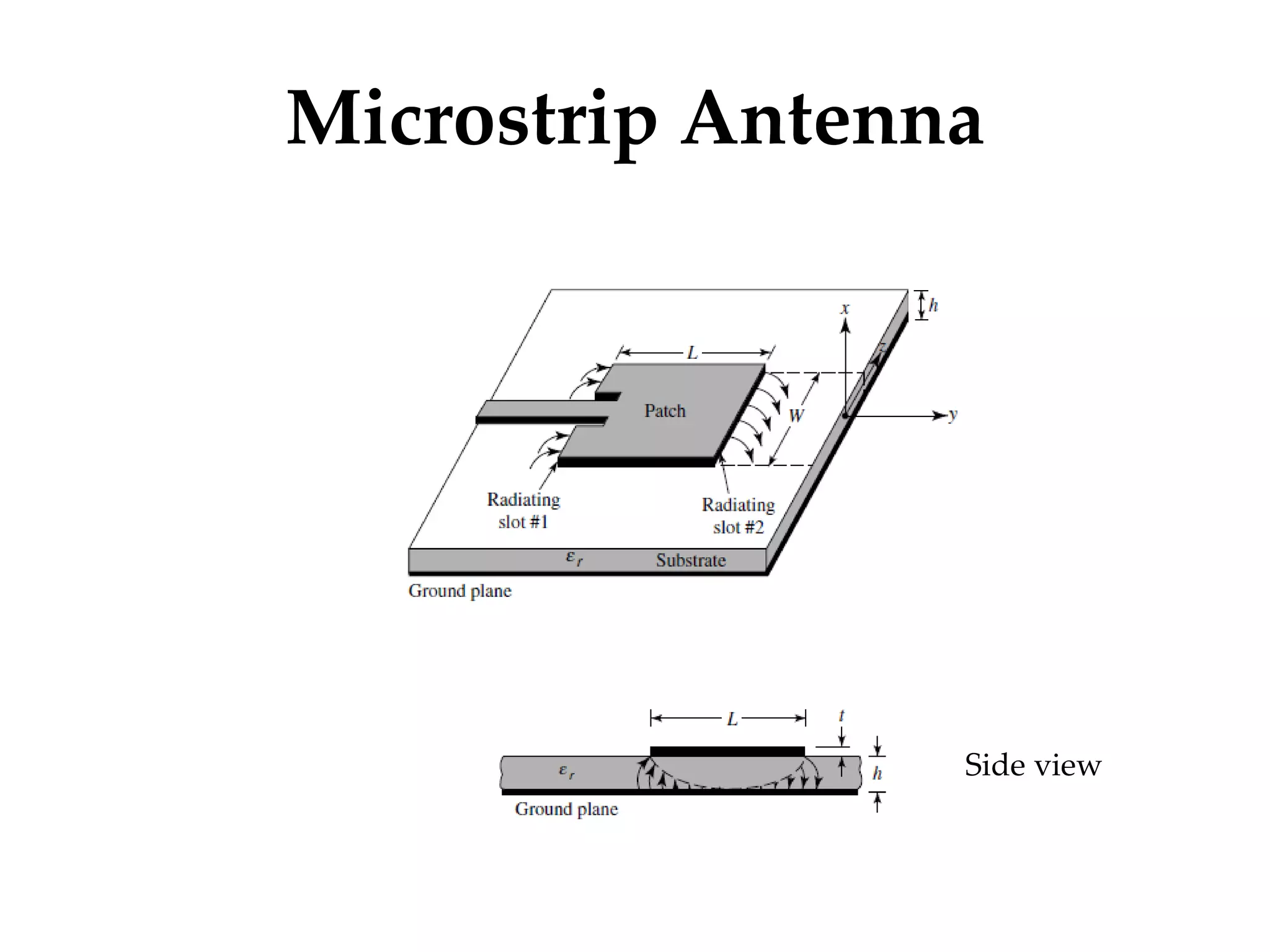
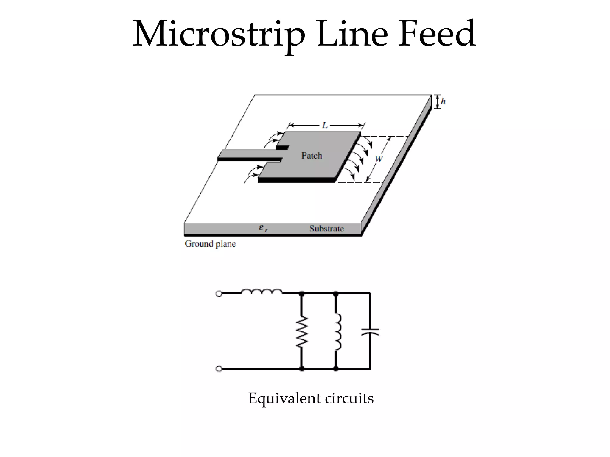
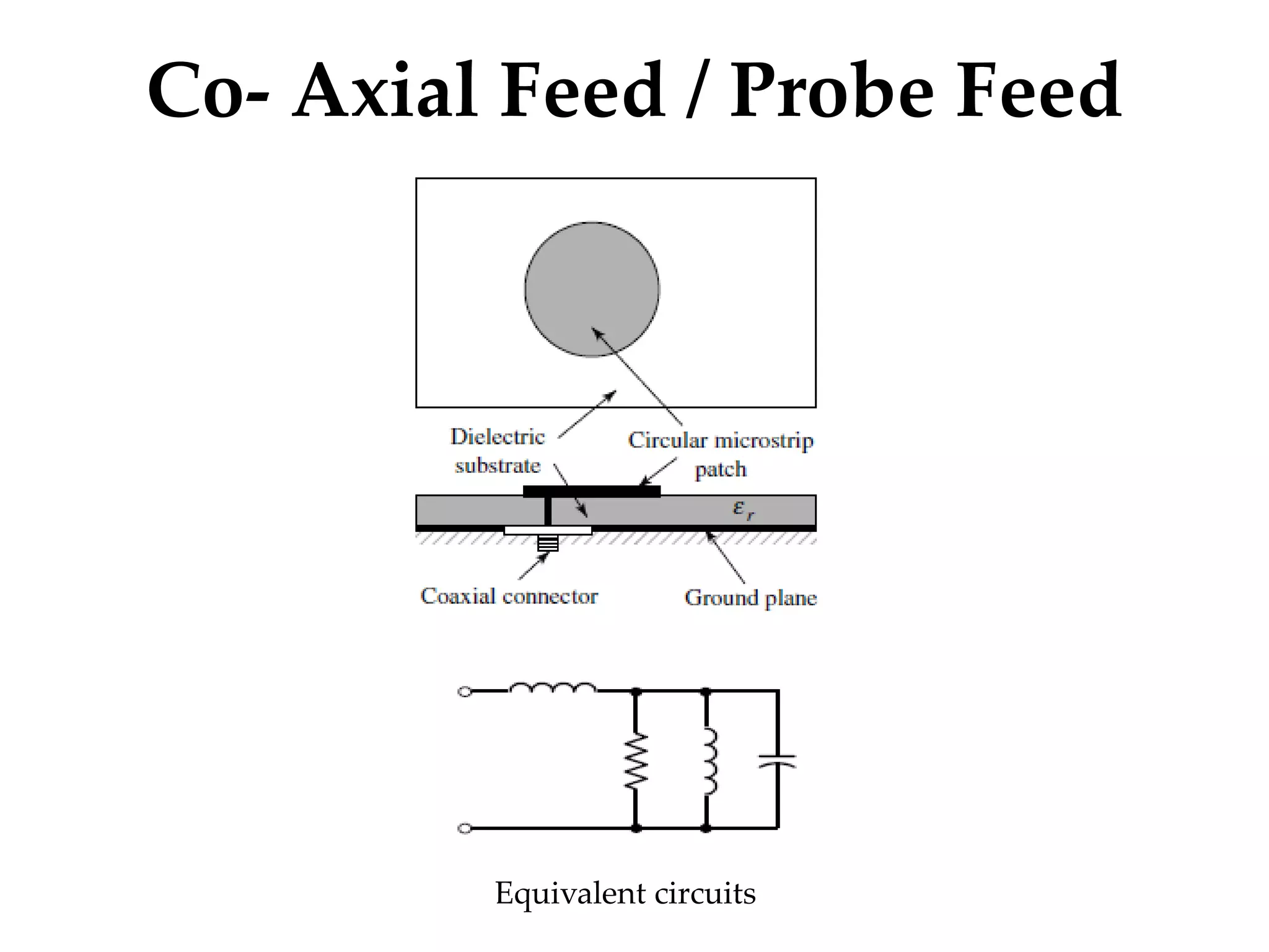
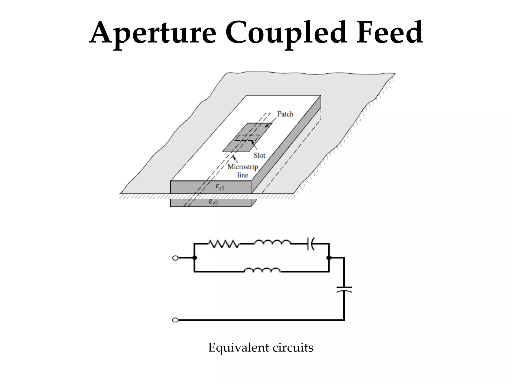
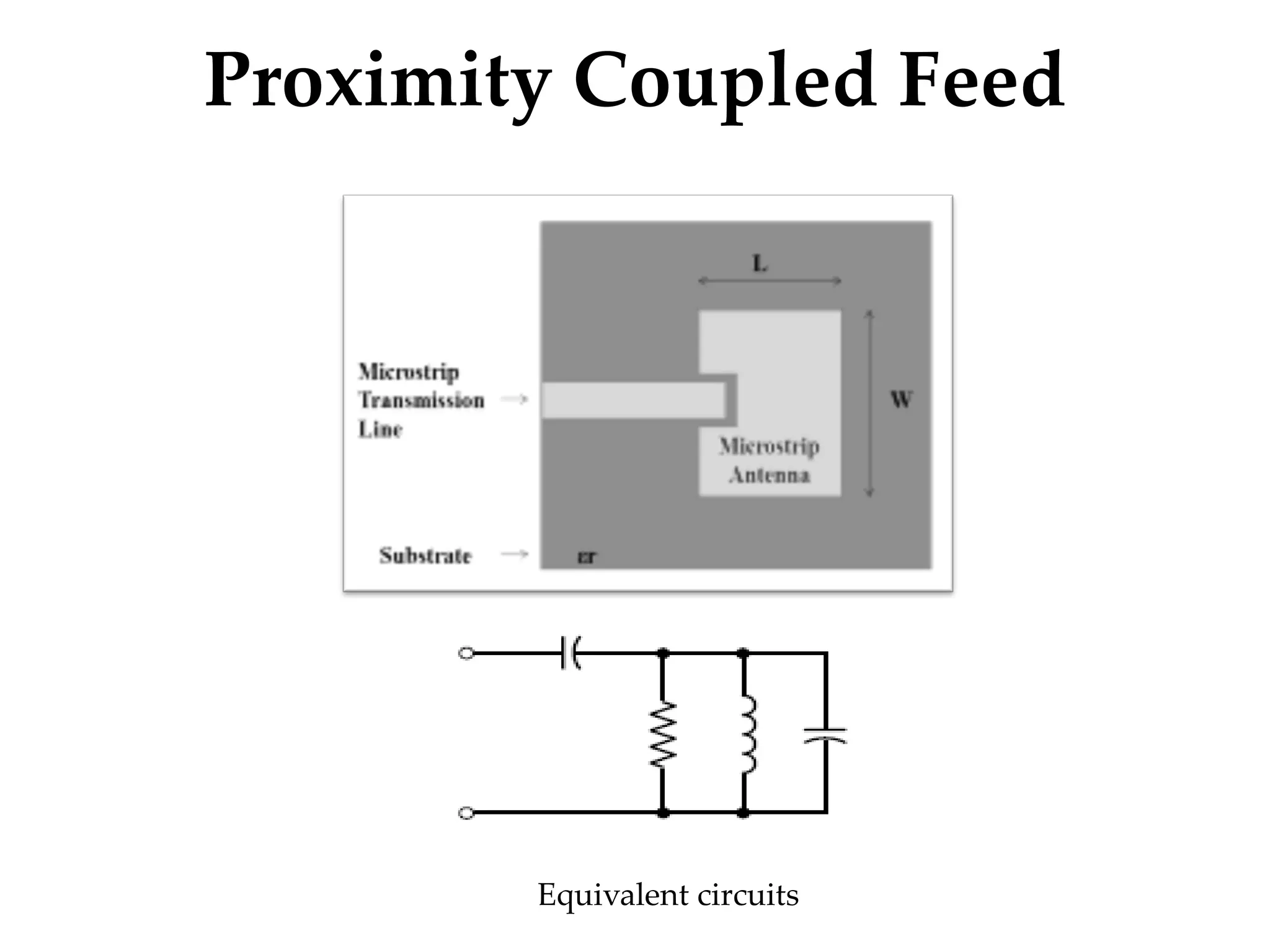
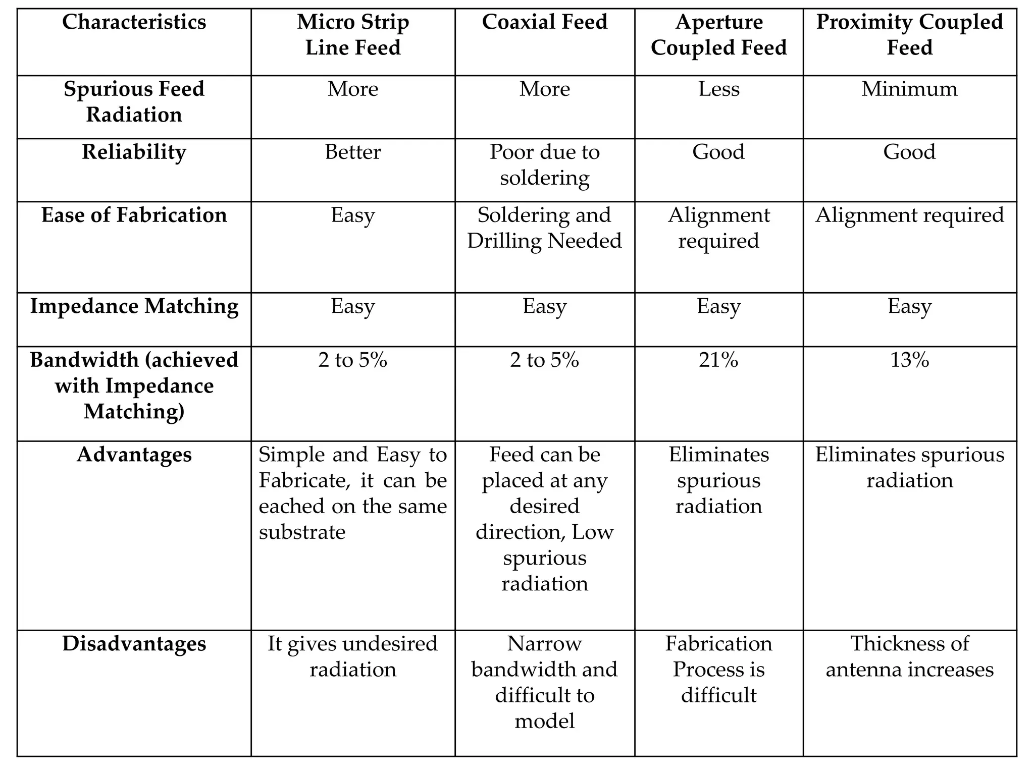

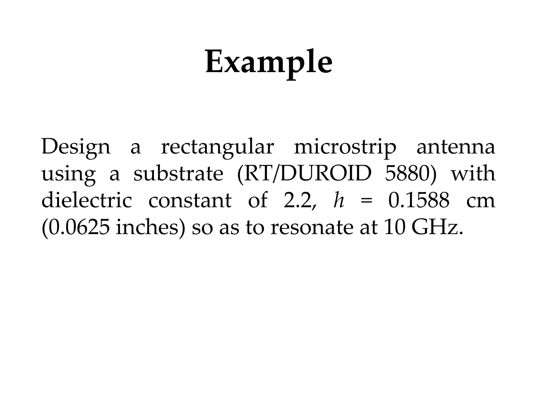
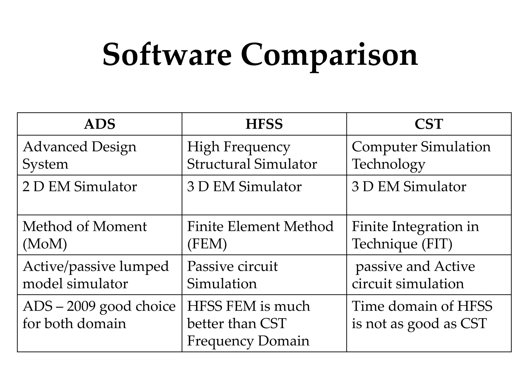

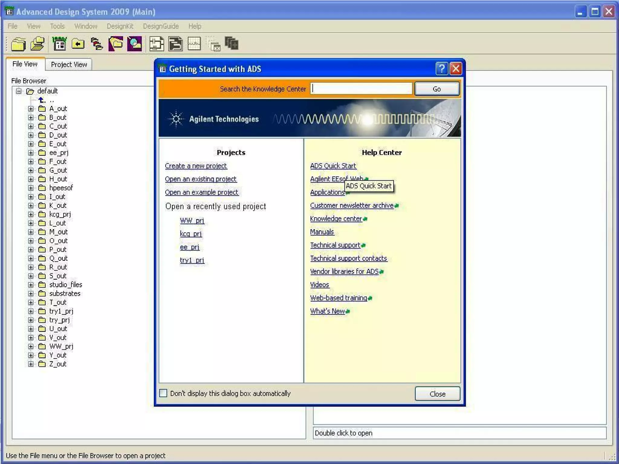
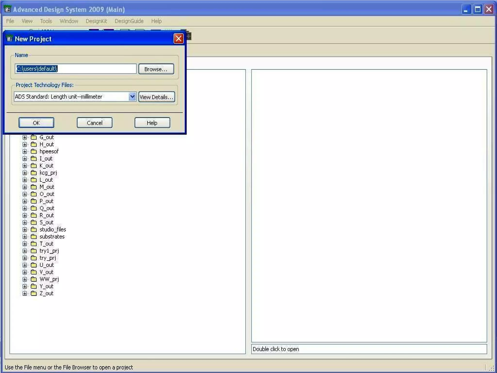
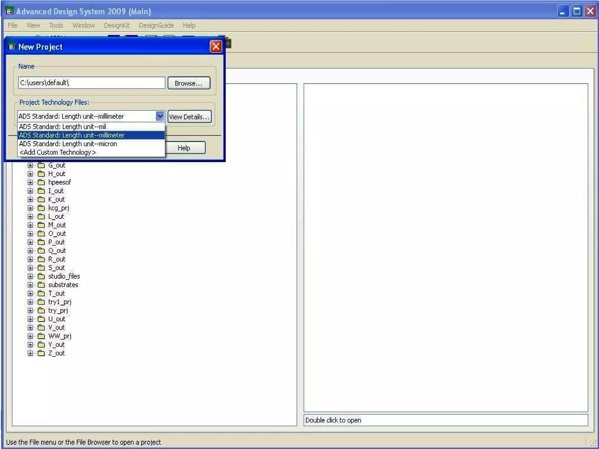
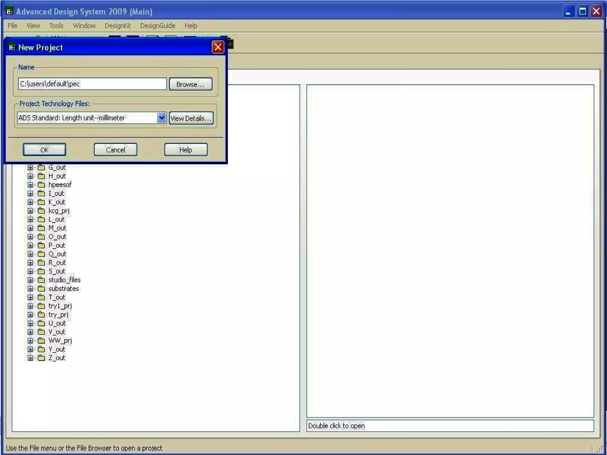
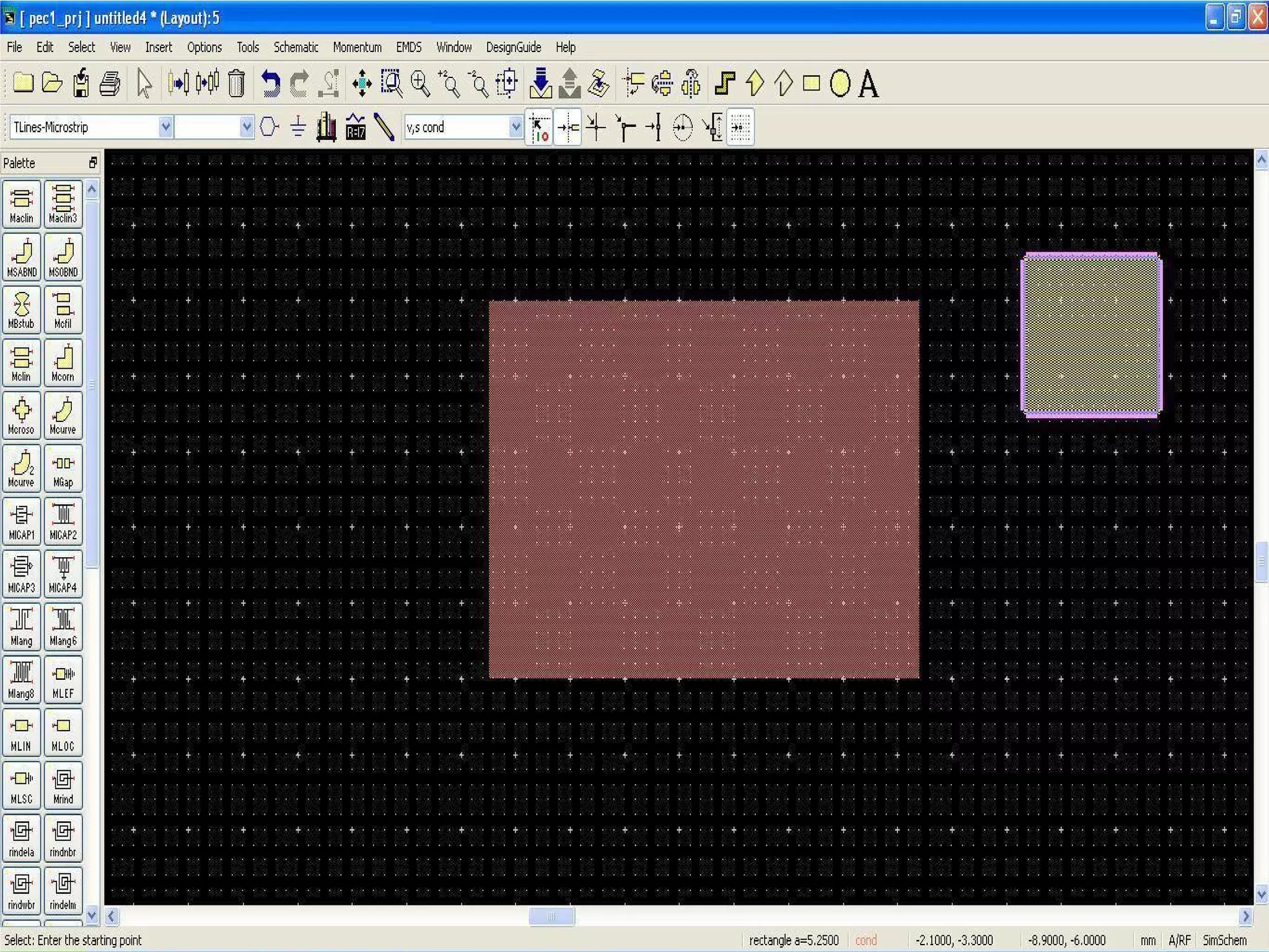
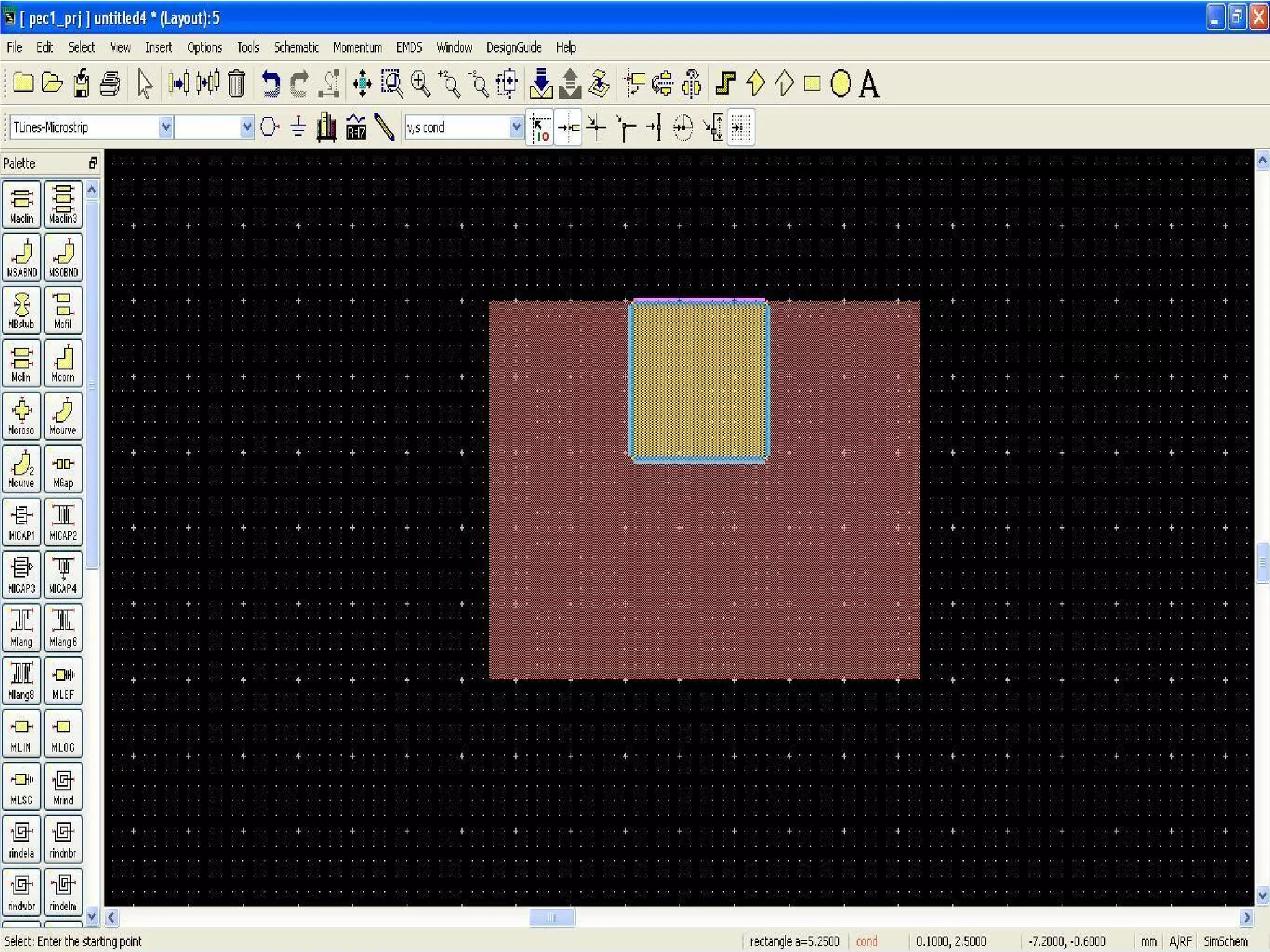
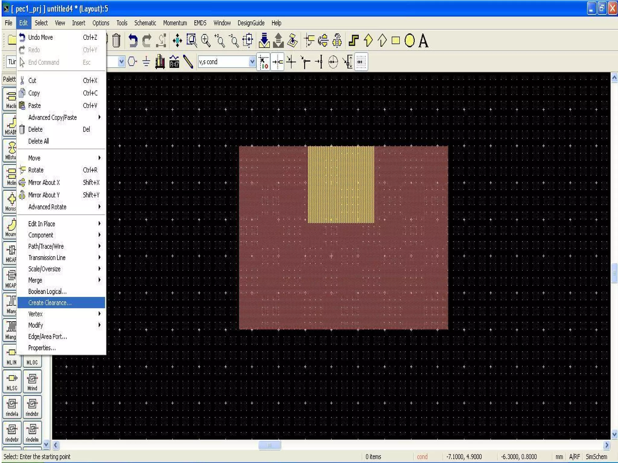
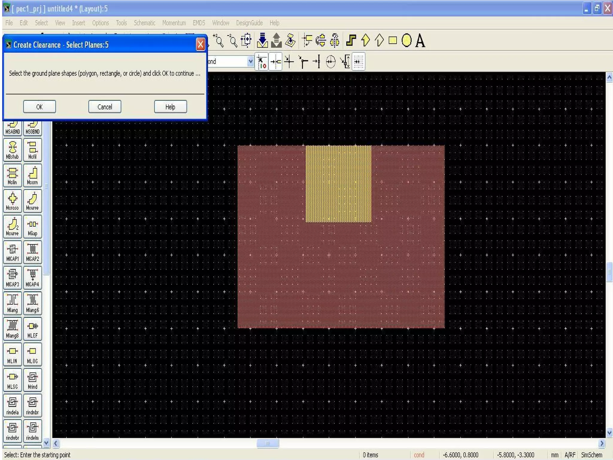
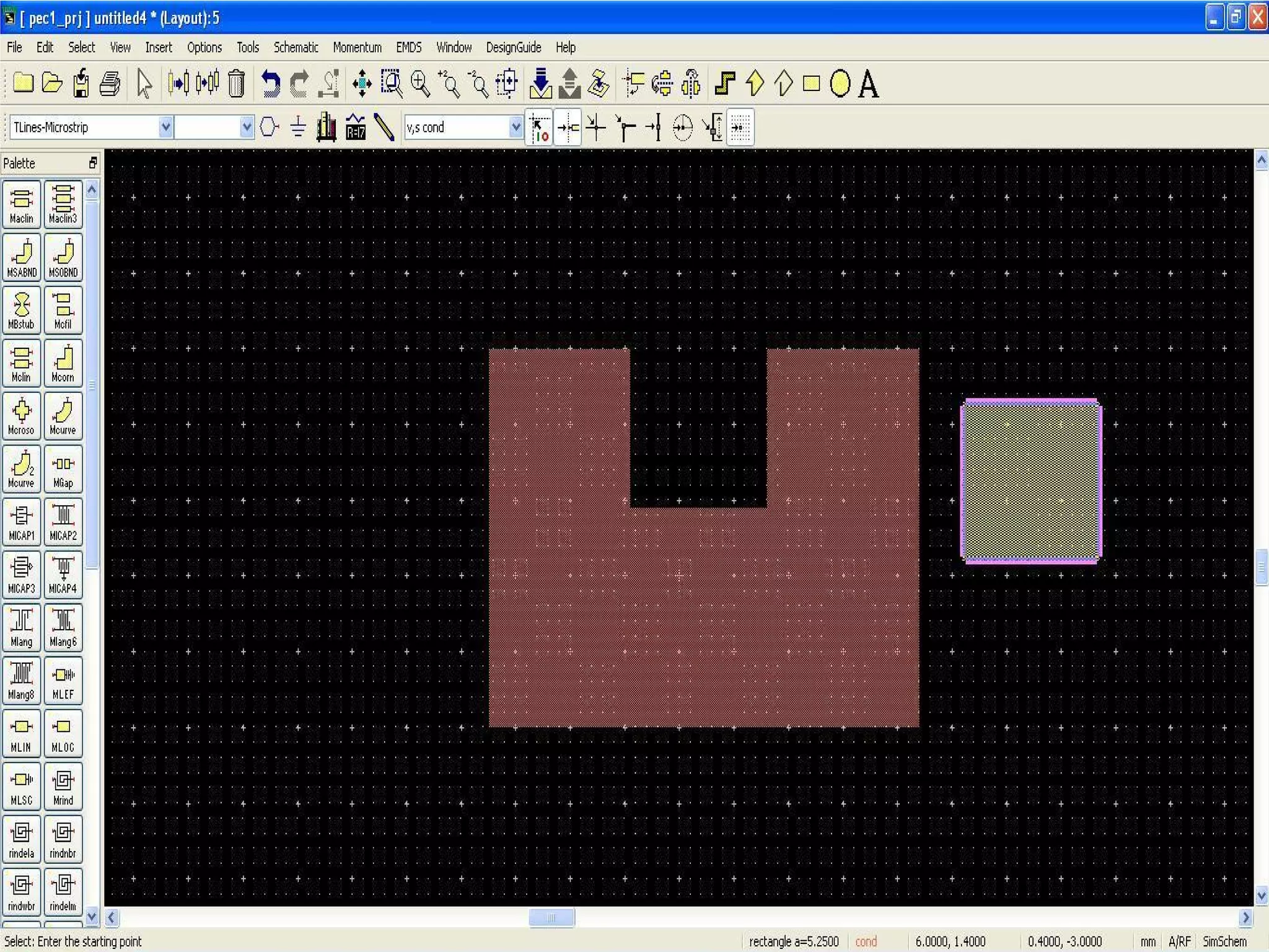
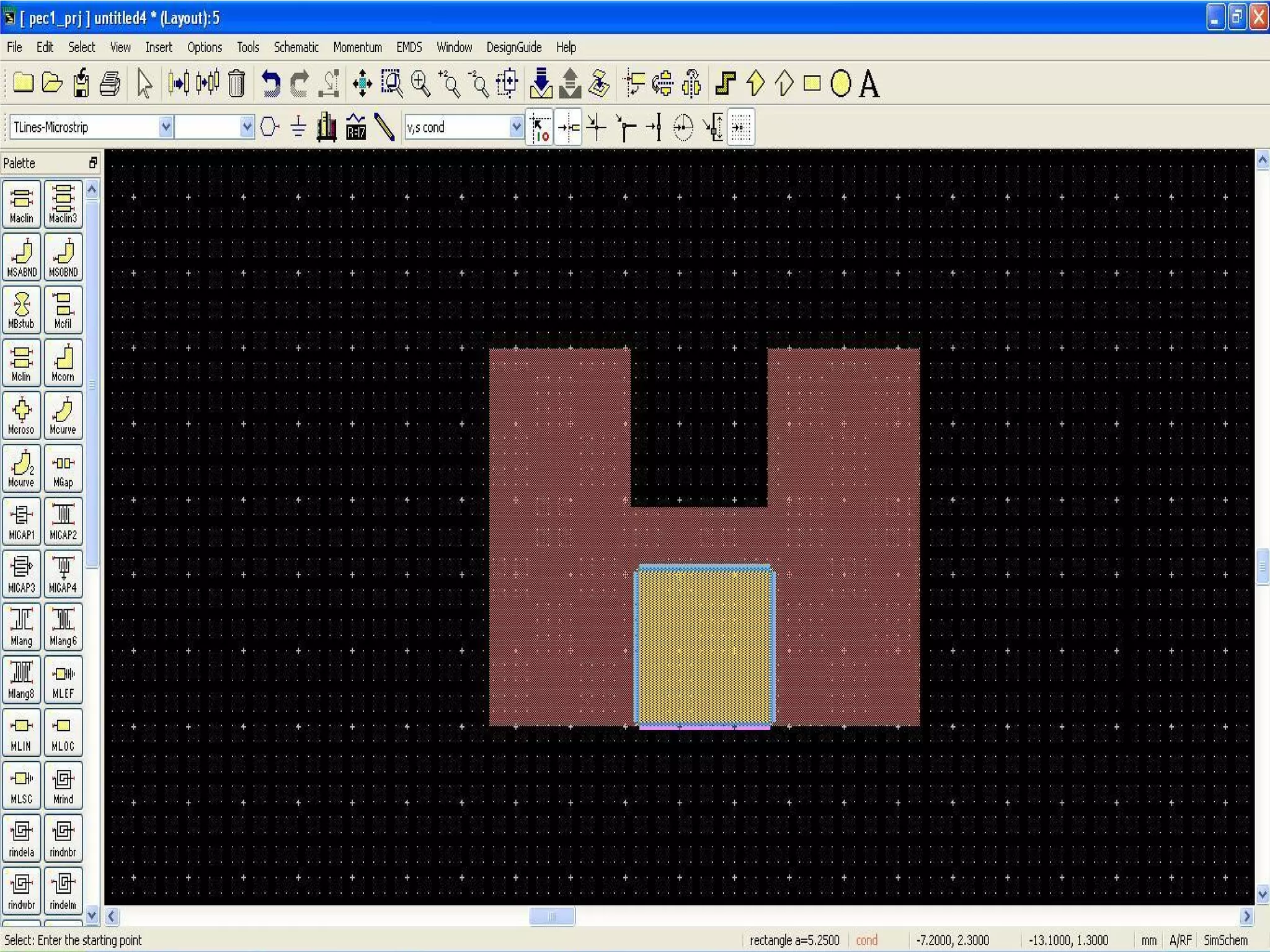
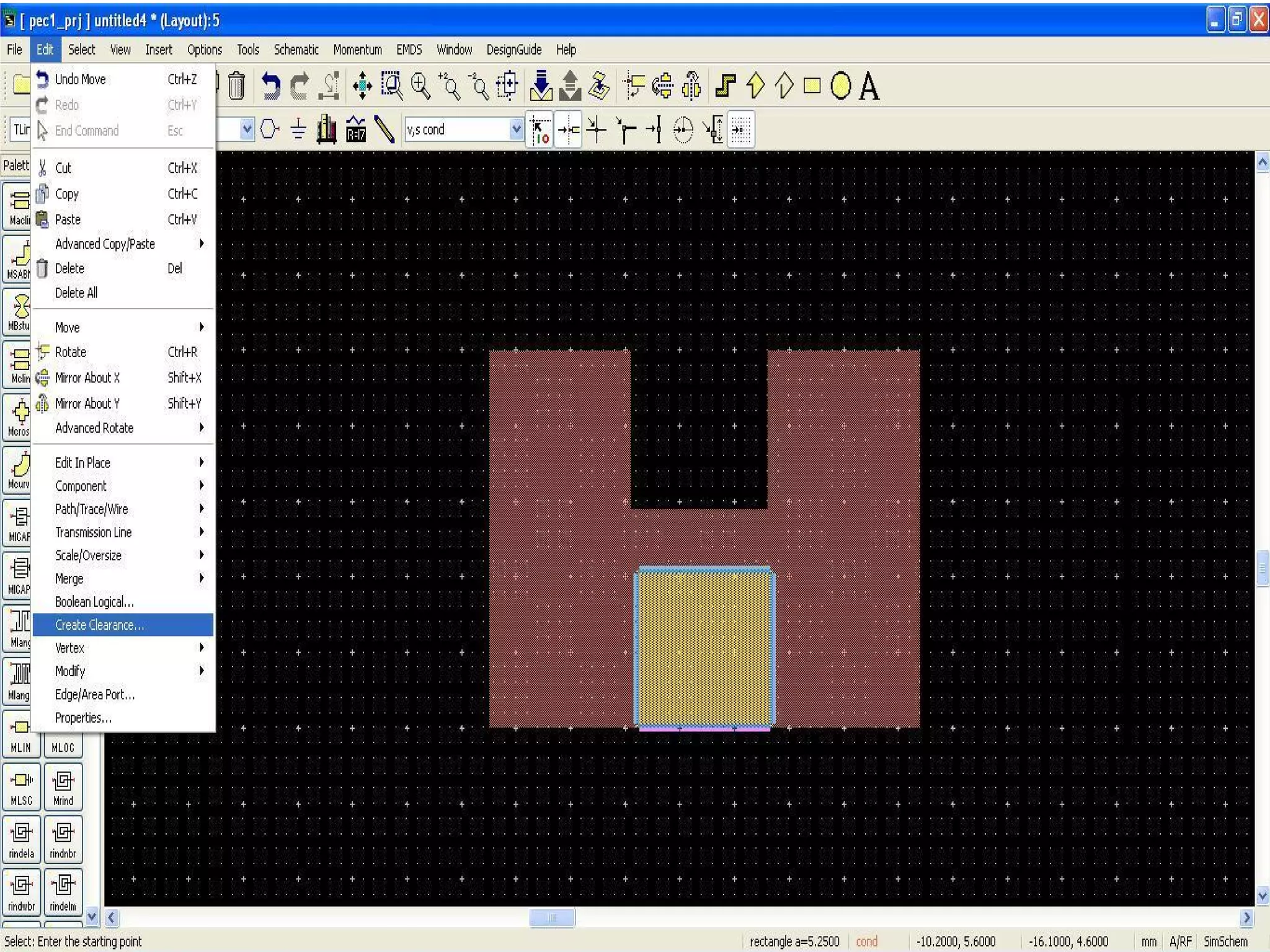
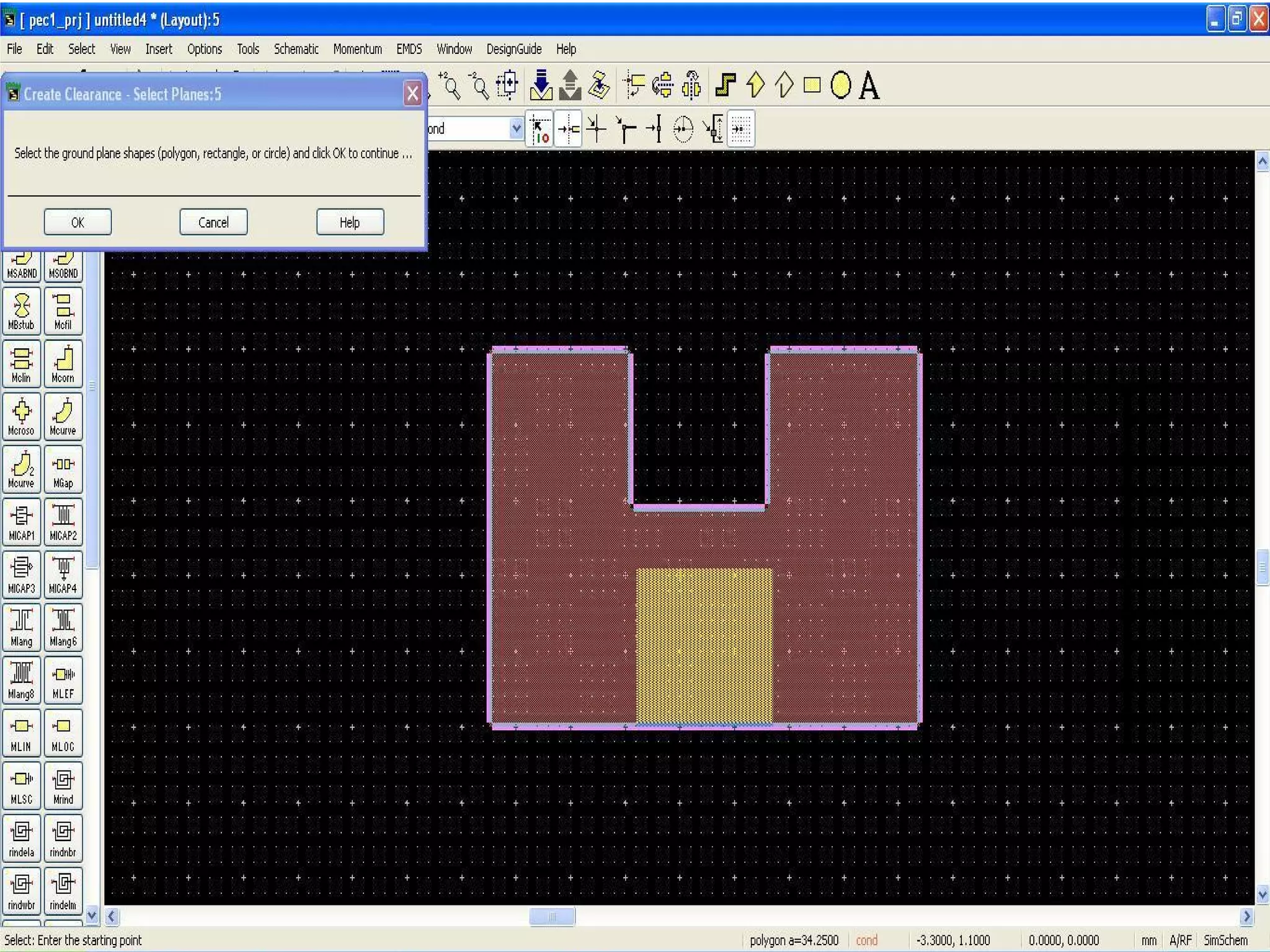
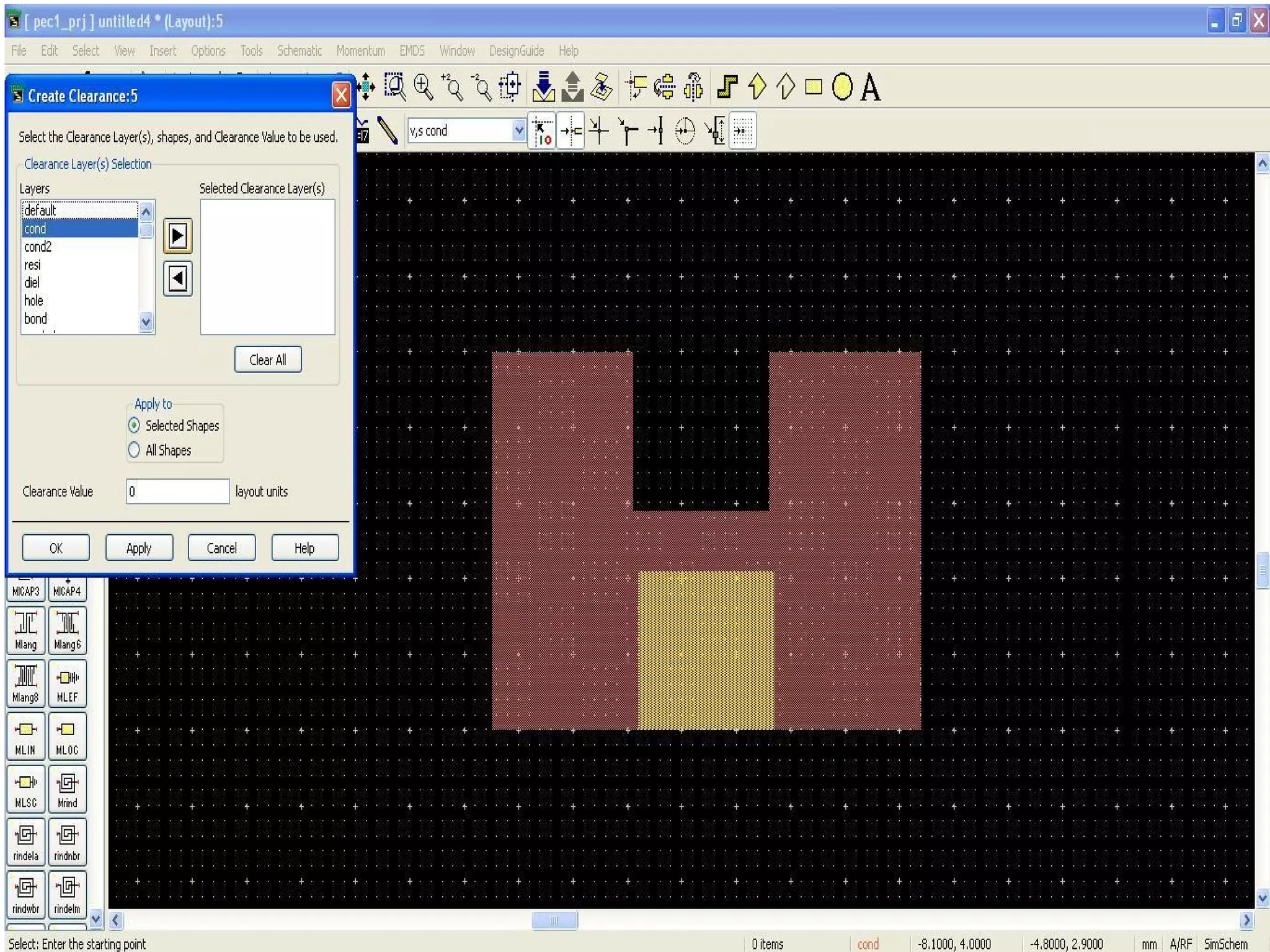
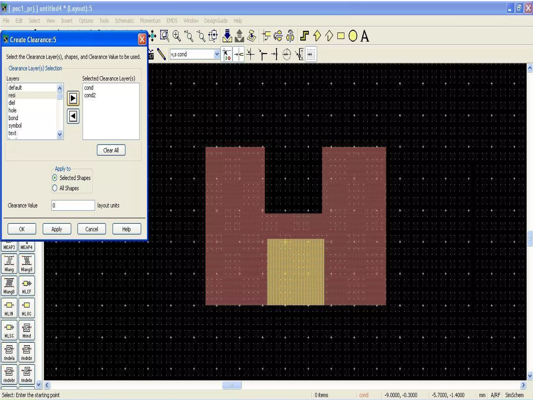
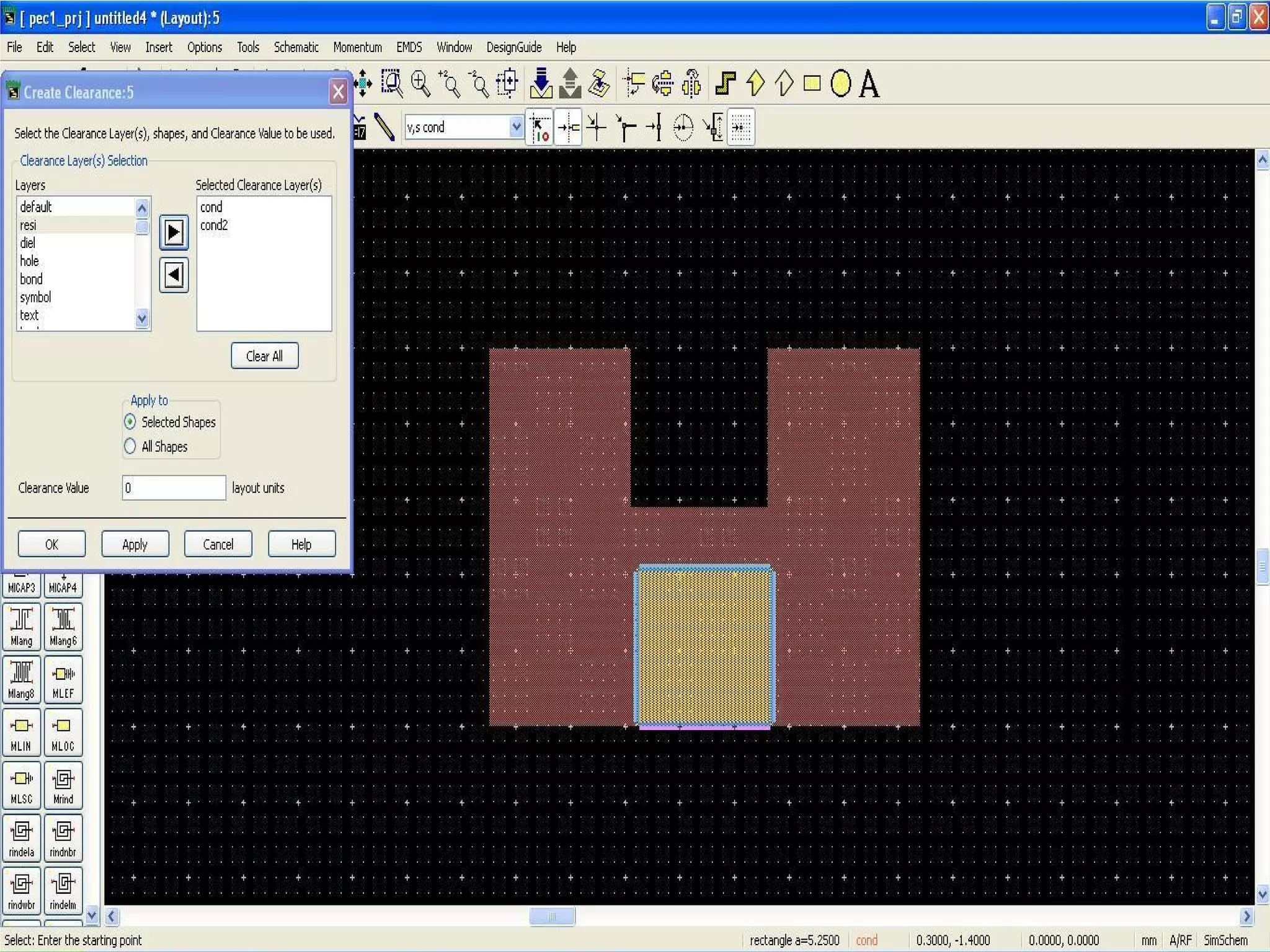
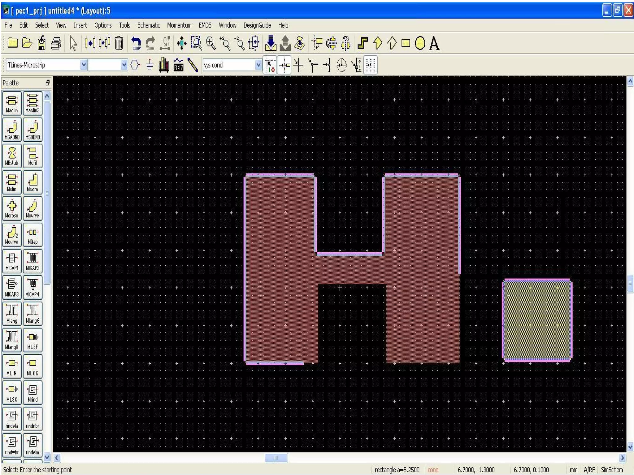


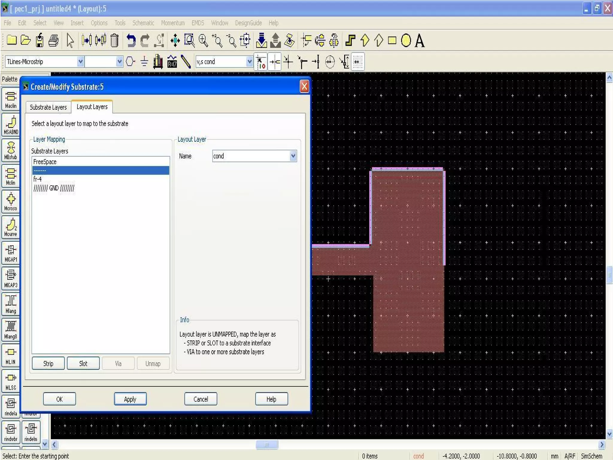
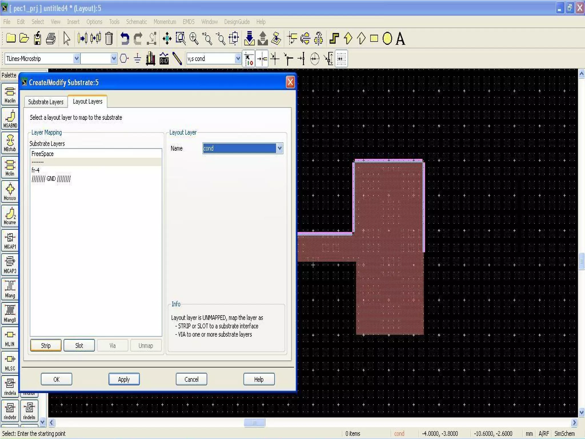
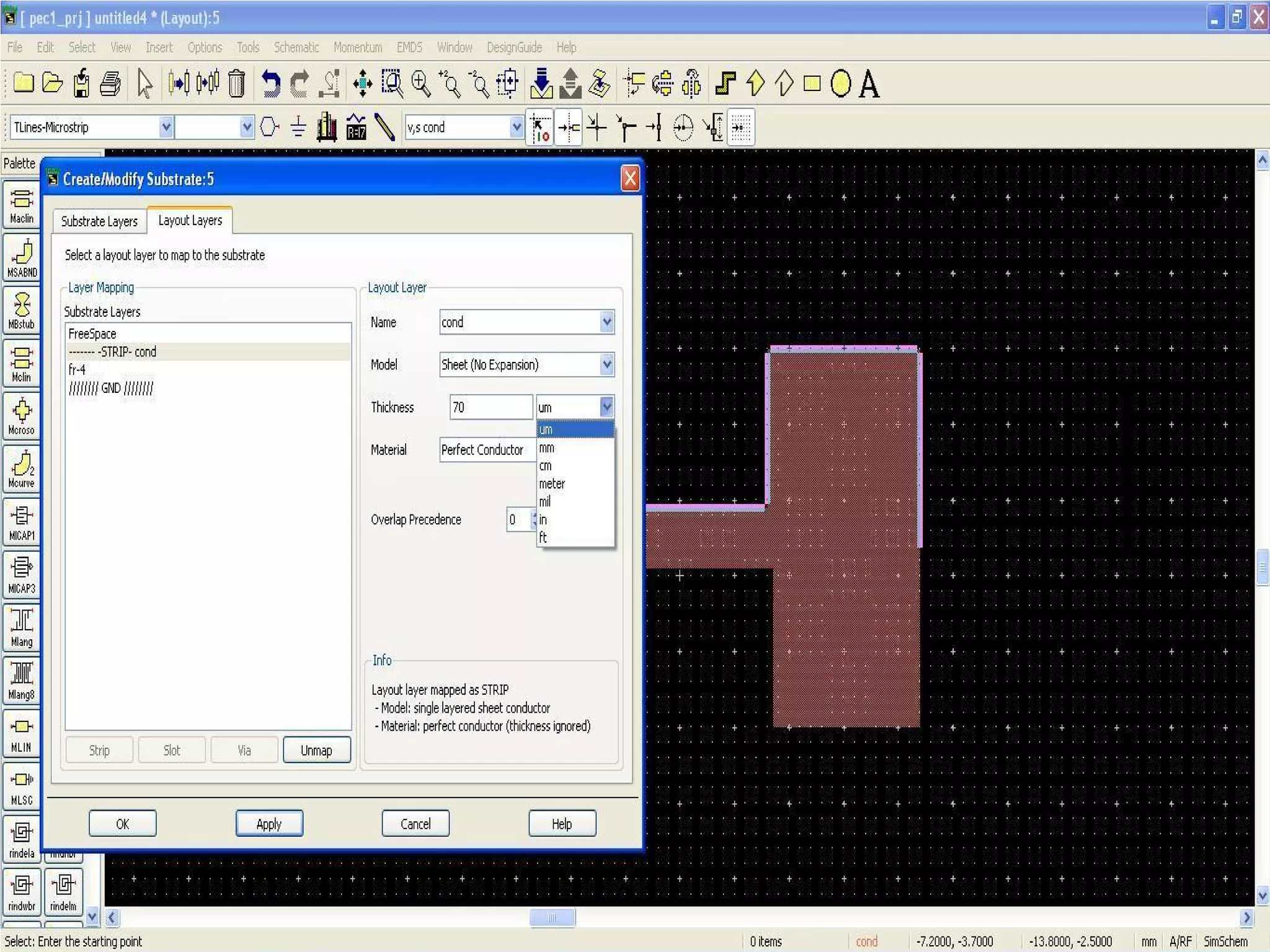
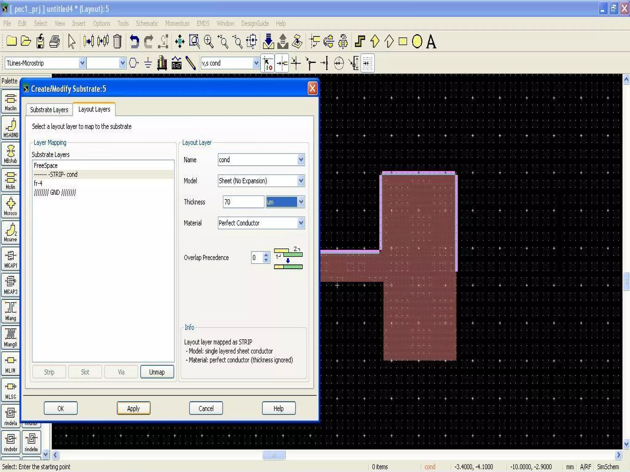
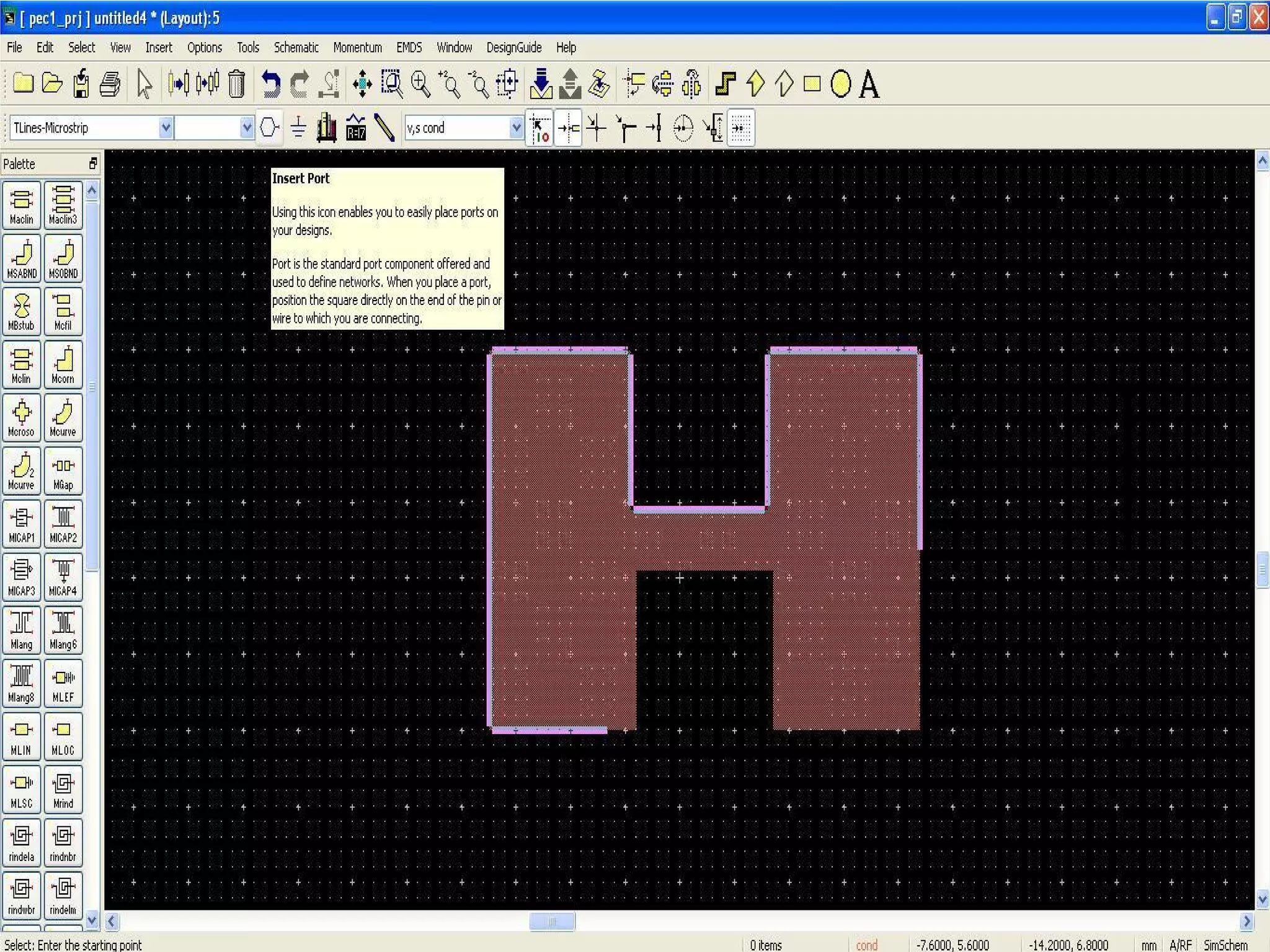
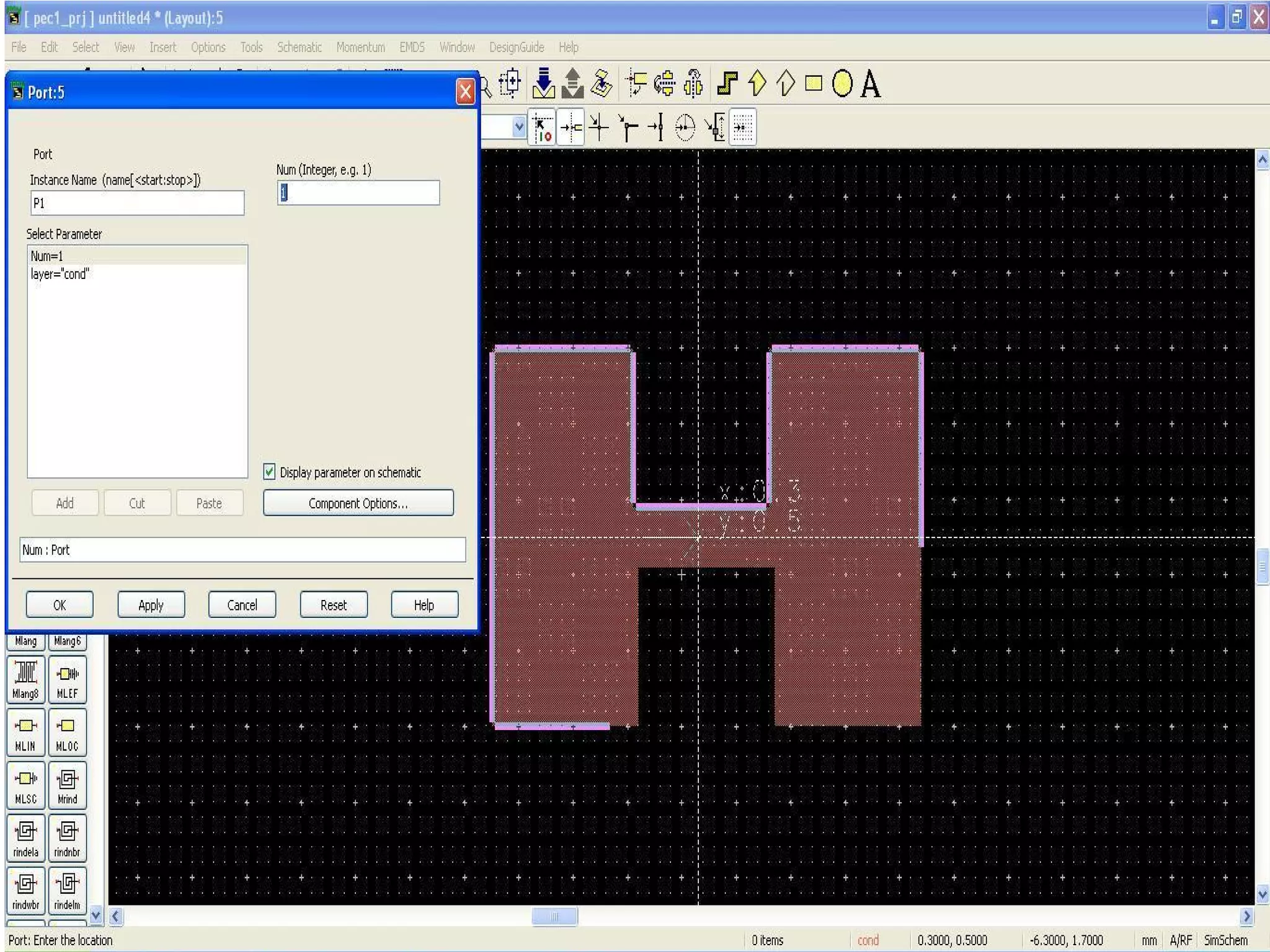
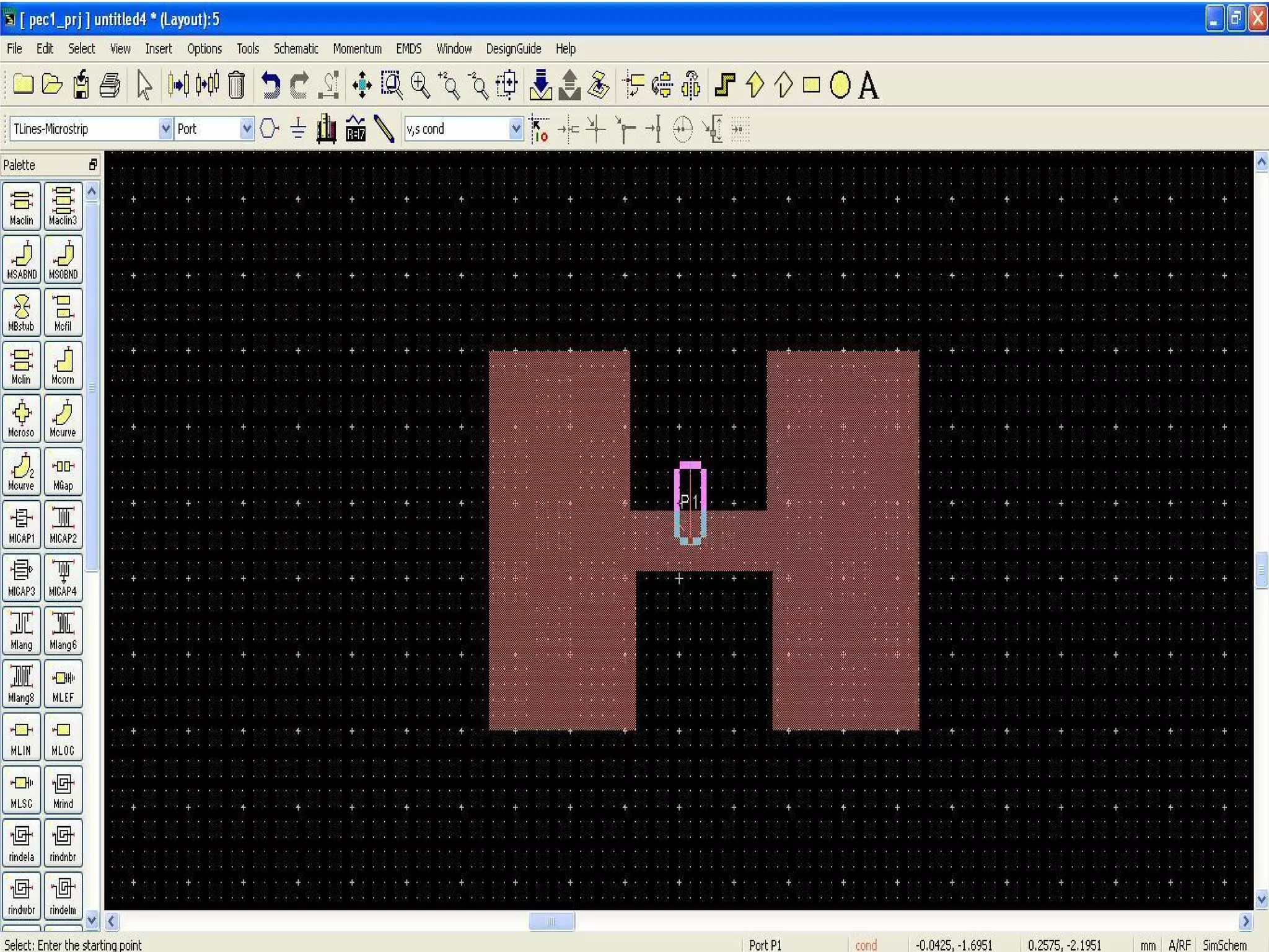
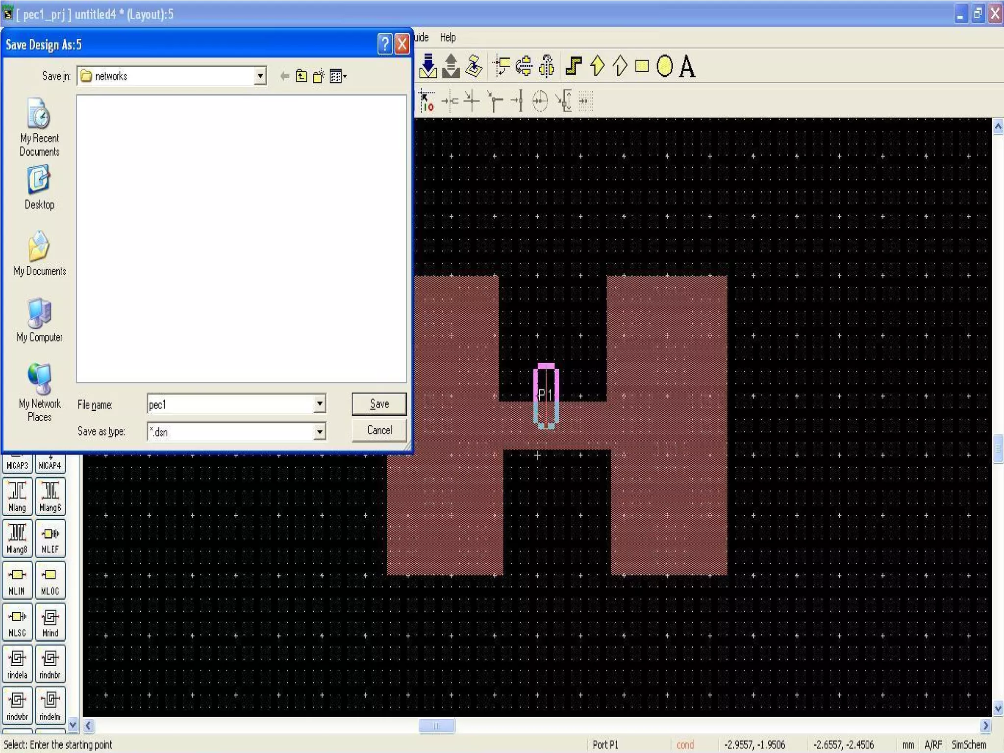


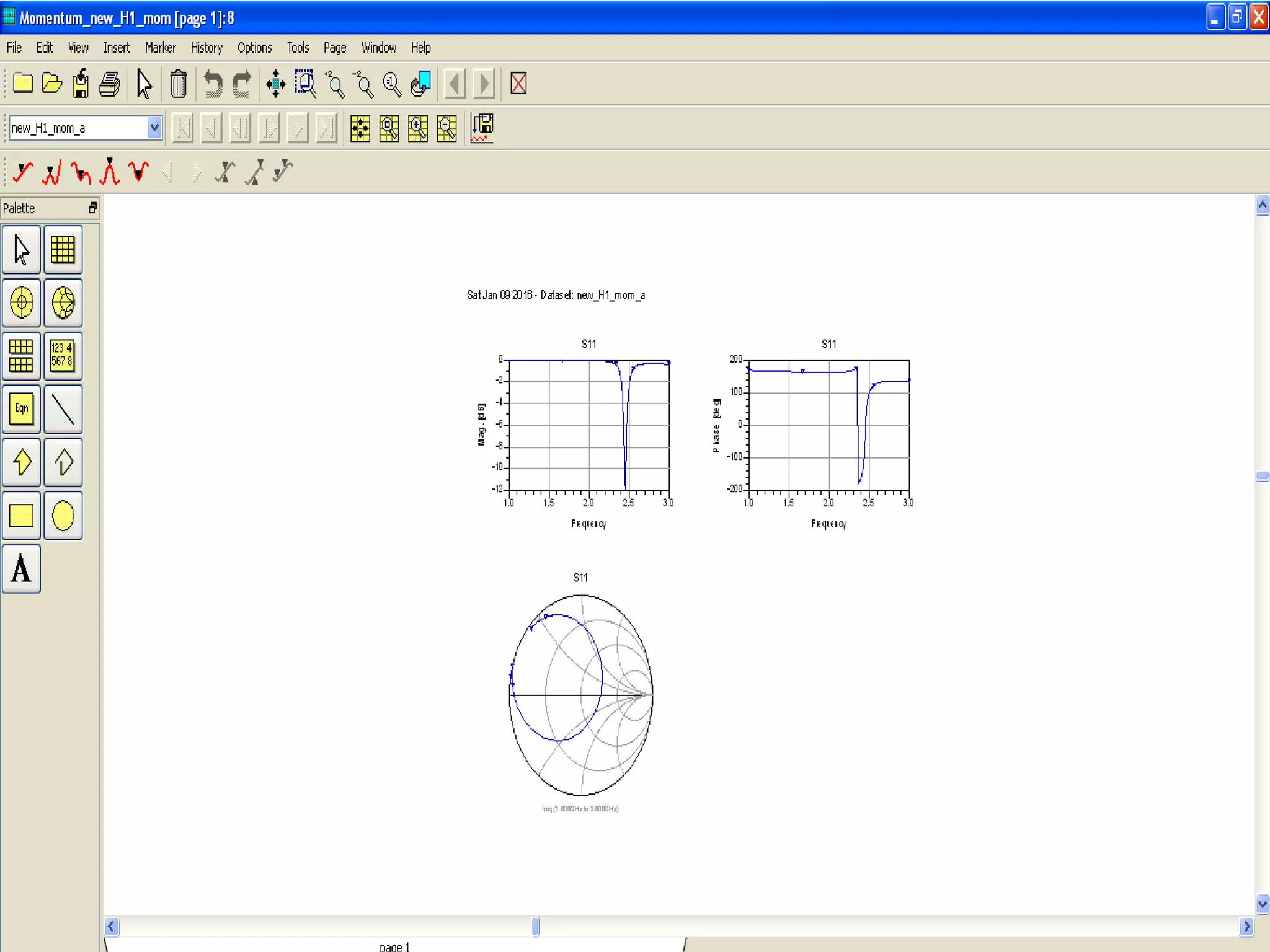

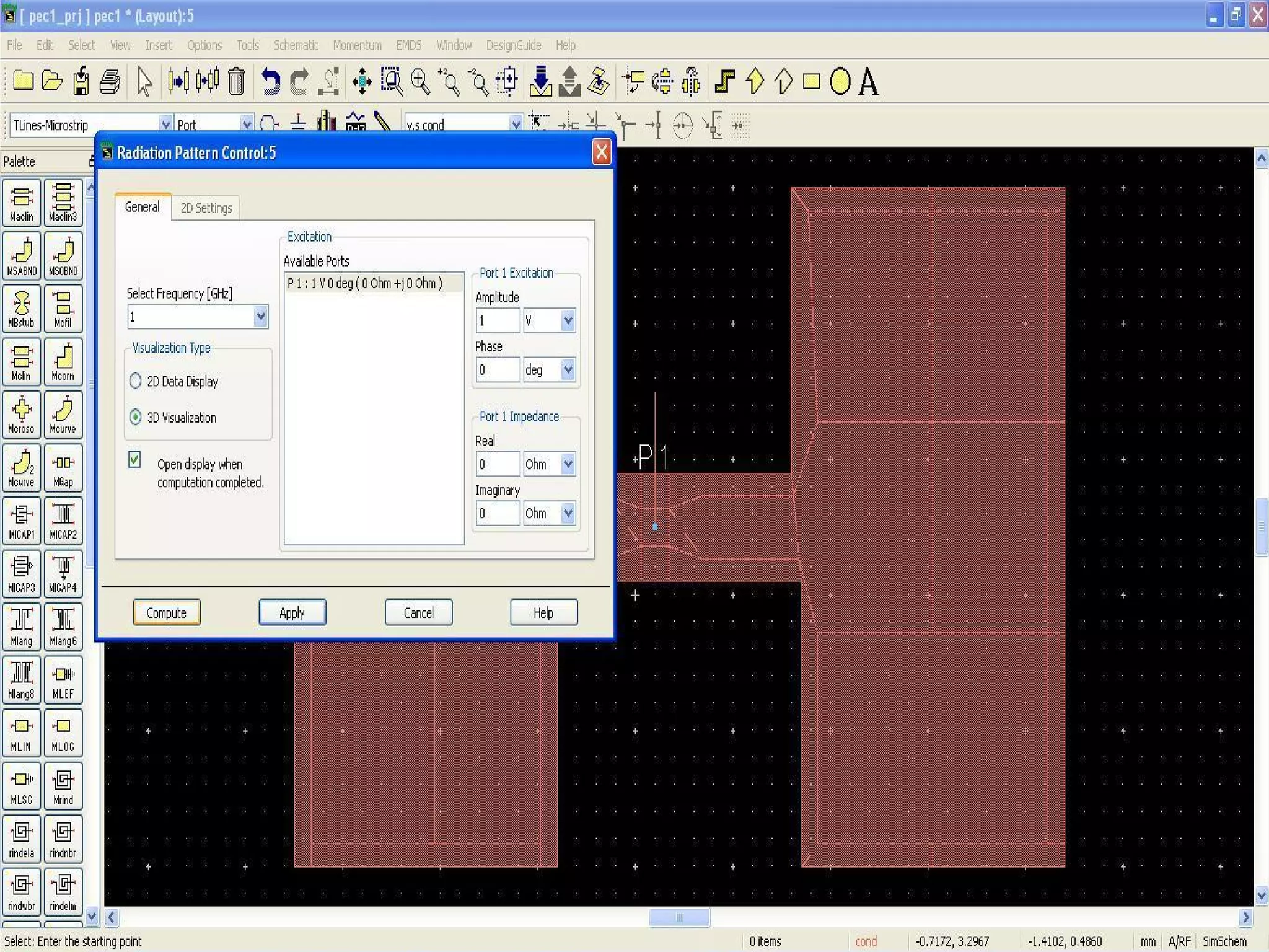
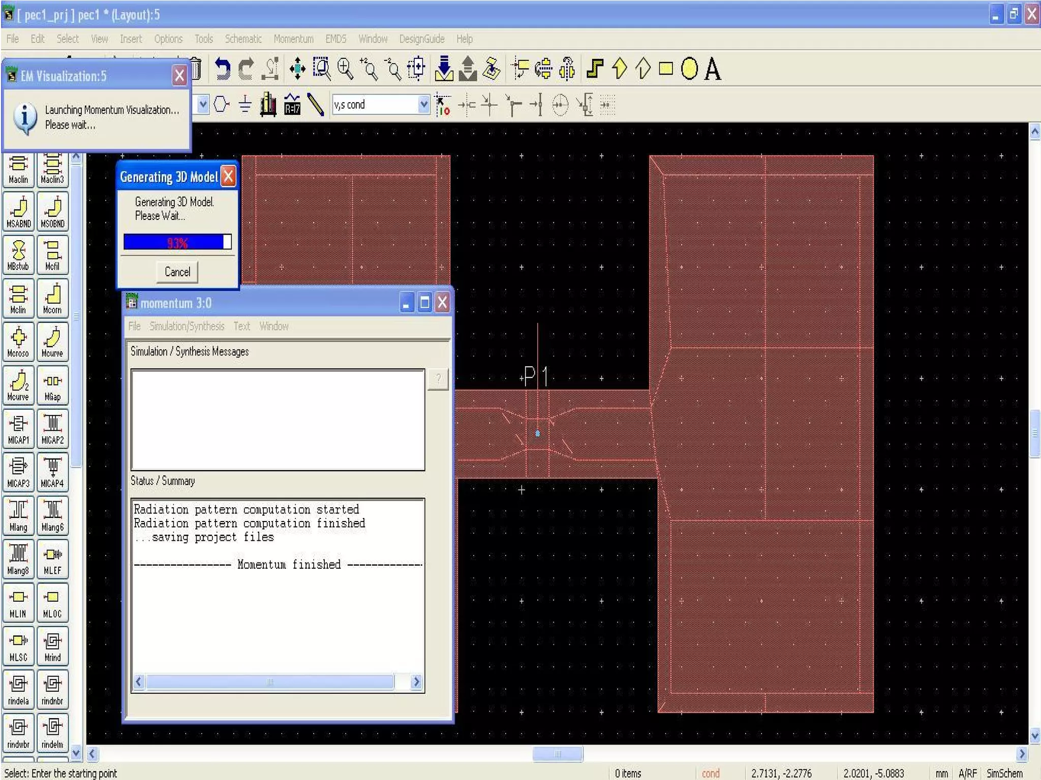
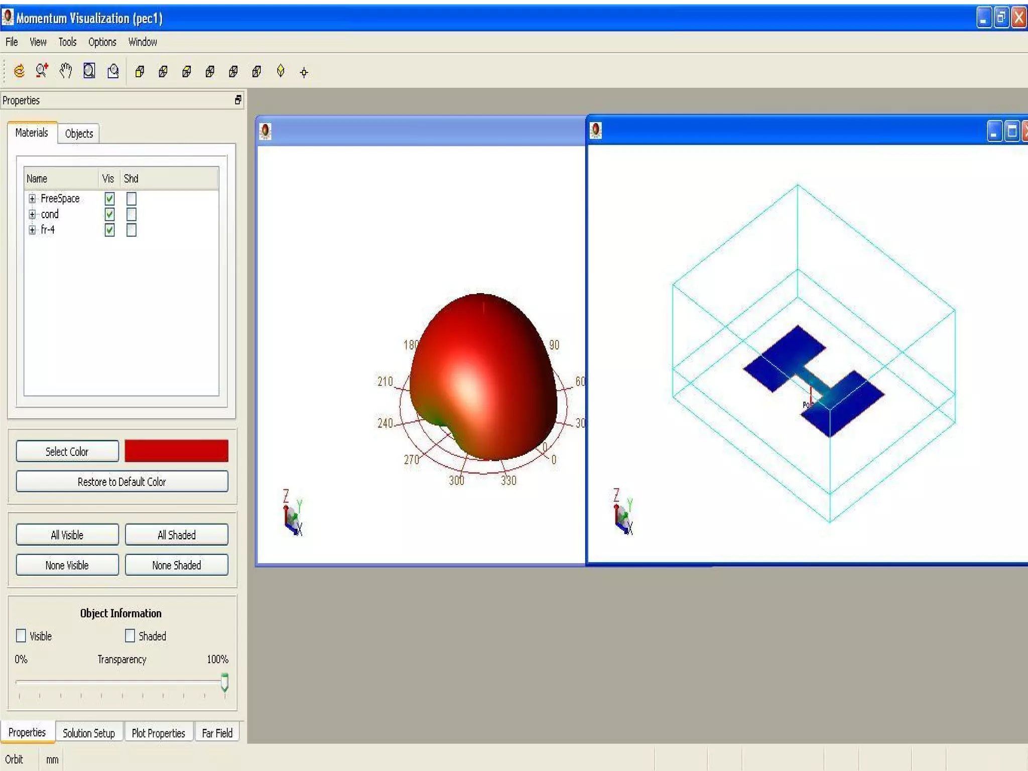
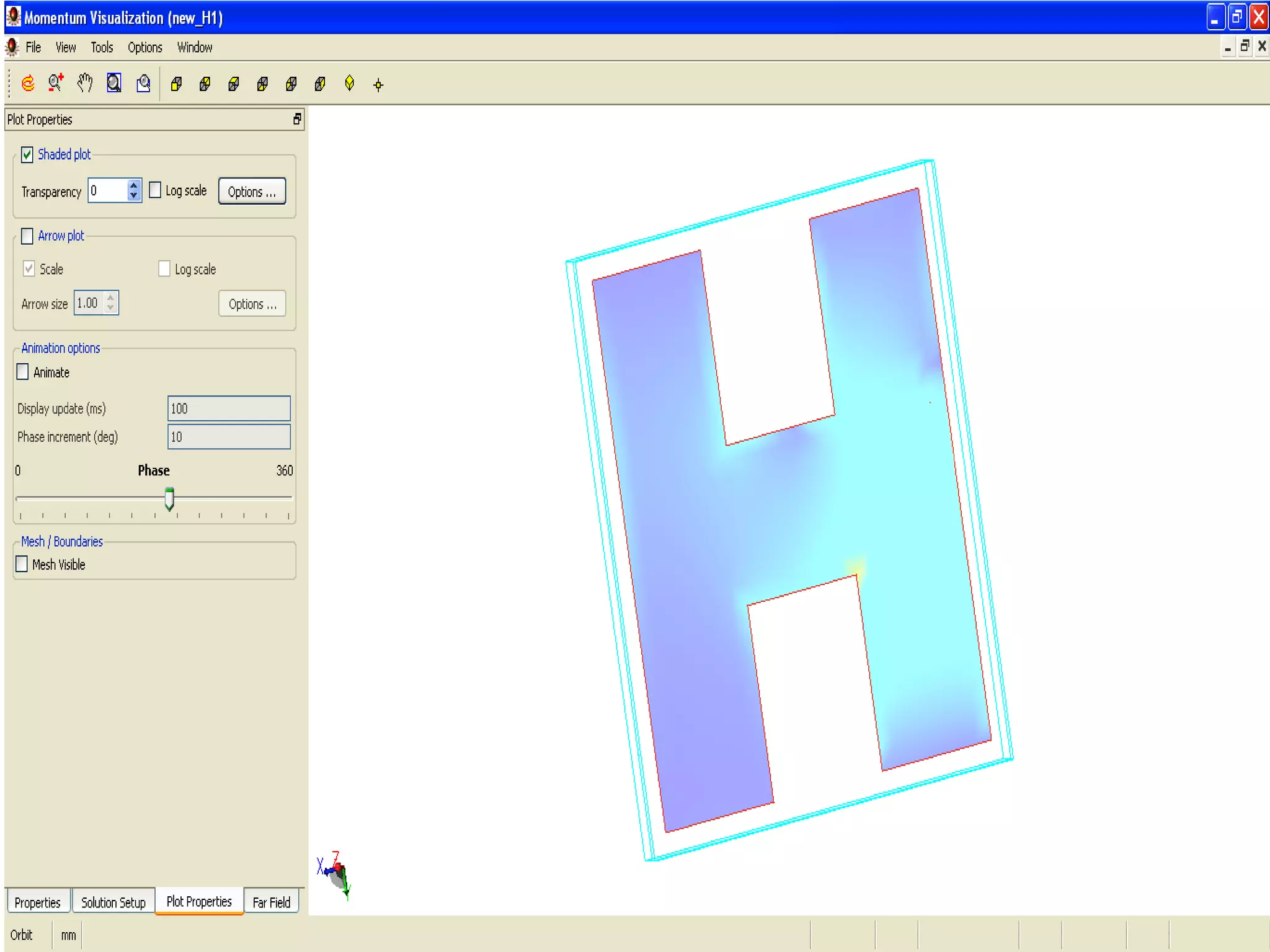
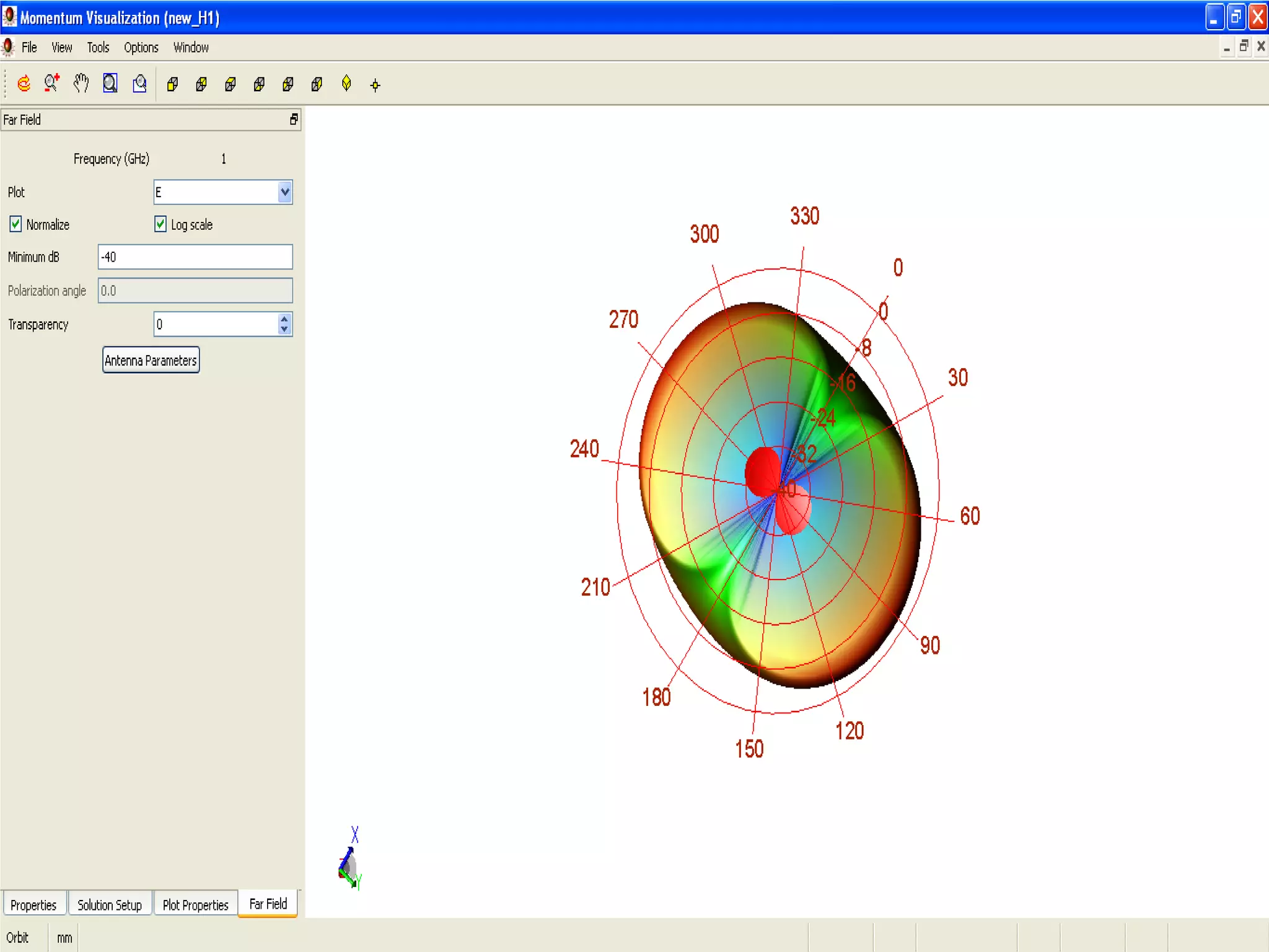
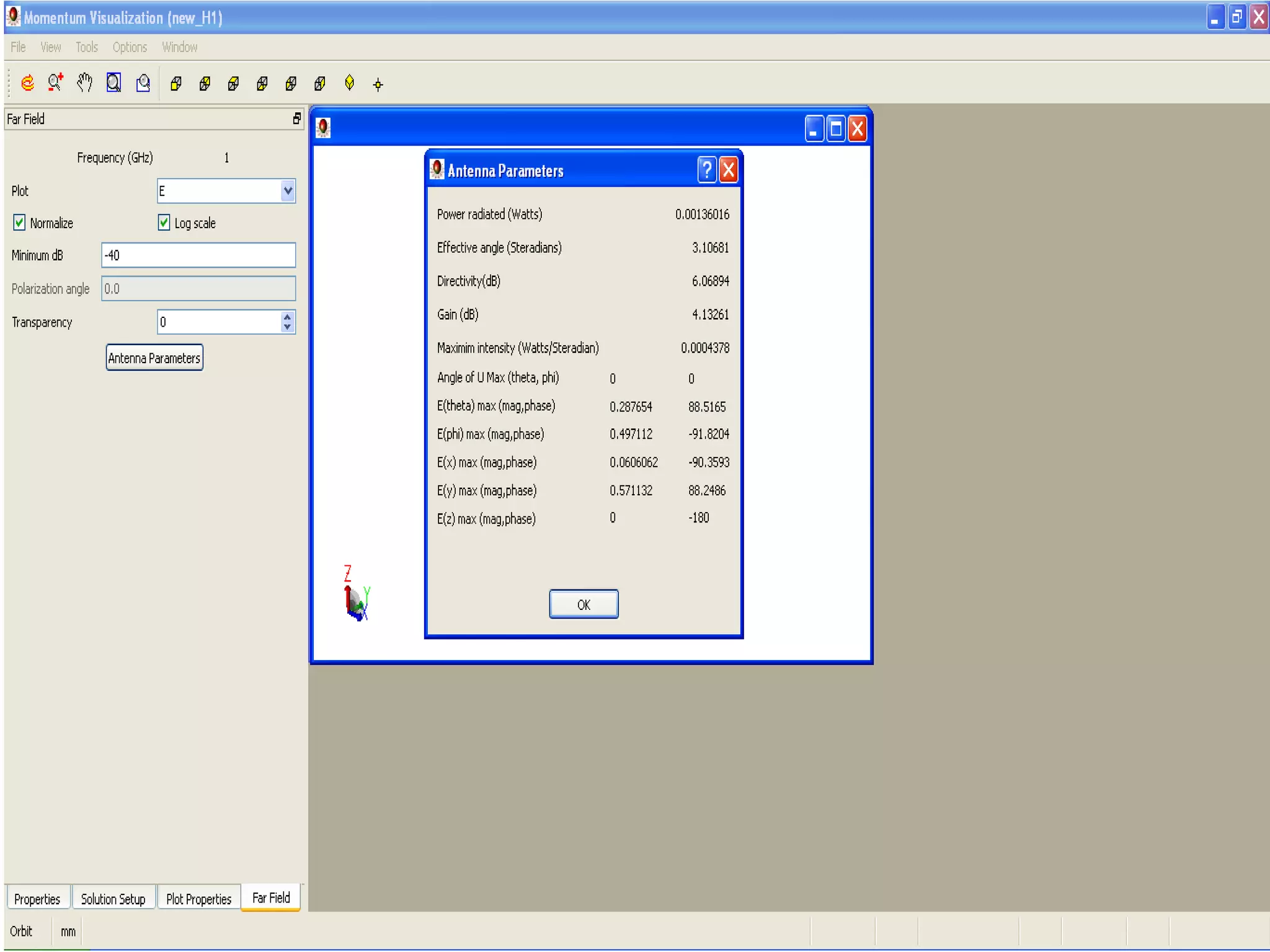


This document provides information on how to design microstrip patch antennas in ADS 2009 software. It discusses different types of microstrip antenna feeds such as microstrip line feed, coaxial feed, aperture coupled feed, and proximity coupled feed. It also compares these different feed types and summarizes their characteristics, advantages, and disadvantages. The document includes an example of designing a rectangular microstrip patch antenna on a dielectric substrate to resonate at 10GHz. It further compares ADS, HFSS, and CST electromagnetic simulation software and recommends ADS 2009 as a good choice for both frequency domain and circuit simulations. Contact information is provided at the end.