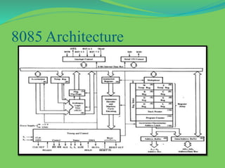
8085Introduction
• It isan 8 bit processor.
• It is a single chip N-MOS device with 40 pins.
• It has multiplexed address and data bus (AD0-AD7).
• It works on 5 volt de power supply.
• The maximum clock frequency is 3 MHz while
minimum frequency is 500MHz.
• It provides 74 instruction with 5 different addressing
modes.
3.
8085 INTRODUCTION
• Itprovides 16 address lines so it can access 2^16=64k
bytes of memory.
• It generates 8 bit I/O address so it can access 2^8=256
input ports.
• It provides 5 hardware interrupts : TRAP, RST5.5, RST
6.5, RST 7.5, INTR.
• It provides ACC, one flag register, 6 general purpose
registers and two special purpose register (SP, PC).
• It provides serial lines SID, SOD. So serial peripherals can
be interfaced with 8085 directly.
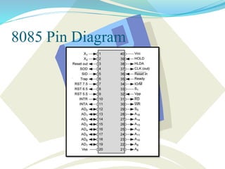
8085 PIN DECRIPTION
SOMEIMPORTANT PINS ARE:
AD0-AD7: Multiplexed address and data lines.
A8- AD15: Tri-stated higher order address lines.
ALE: Address latch enable is an output signal. It goes high
when operation is started by processor.
S0-S1: These are the status signals used to indicate type of
operation.
RD: Read is active low input signal used to read data from I/O
device or memory.
WR: Write is an active low output signal used write data on
memory or an I/O device.
6.
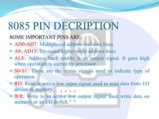
8085 PIN DECRIPTION
READY:This is an output signal used to check the status of
output device. If it is low, up will wait until it is high.
TRAP: It is an edge triggered highest priority, non mask
able interrupt. After TRAP, restart occurs and execution
starts from address 0024H.
RST5.5,6.5,7.5: Those are maskable interrupts and have low
priority than TRAP.
INTR-&INTA: INTR is a interrupt request signal after
which up generates INTA or interrupt acknowledge signal.
IO/M-: This is output pin or signal used to indicate memory
mode(IO/M=0).
7.
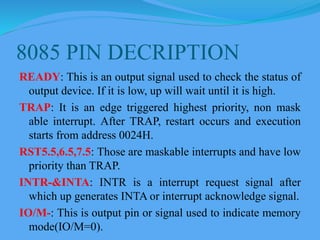
8085 PIN DECRIPTION
HOLD&HLDA:HOLD is an input signal. When Up receives
hold signal it completes current machine cycle and stops
executing next instruction. In response to hold up generating
HLDA that is HOLD Acknowledge signal.
RESET IN-: This is input signal .When RESET IN- is low up
restarts and starts executing from location 0000H.
SID: Serial input data is input pin used to accept serial 1 bit
data.
X1X2: These are clock input signals and are connected to
external LC, or RC circuit. These are divide by two so if 6
MHz is connected to x1x2, the operating frequency becomes 3
MHz .
Arithmetic and LogicalGroup
Accumulator: It is 8 bit general purpose register .
• It is connected to ALU.
• So most of the operations are done in Acc.
Temporary register : It is not available for use. All the
arithmetic and logical operations are done in the
temporary register but user can’t access it.
10.
FLAG REGISTER
These arethe set of 5 flip- flops:-
Sign (S)
Zero (Z)
Auxiliary carry (AC)
Parity(P)
Carry (C)
11.
TIMING AND CONTROLUNIT
Control Signals: READY, RD’,WR’, ALE
Status Signals:S0,S1,IO/M’
DMA Signals: HOLD, HLDA
RESET Signals: RESET IN, RESET OUT
![“MICROPROCESSOR ARCHITECTURE"
AKS UNIVERSITY
[SESSION 2017]
SUBBMITTED BY SUBMITTED TO
MR. AKSHAY JAIN MR.BRIJESH K. SONI
BSC(CS) 1ST SEM ASSISTANT PROFESSOR
DEPTT. OF PHYSICS DEPTT. OF COMPUTER](https://image.slidesharecdn.com/akshayjain-171124070453/85/Microprocessor-Architecture-8085-1-320.jpg)
![“MICROPROCESSOR ARCHITECTURE"
AKS UNIVERSITY
[SESSION 2017]
SUBBMITTED BY SUBMITTED TO
MR. AKSHAY JAIN MR.BRIJESH K. SONI
BSC(CS) 1ST SEM ASSISTANT PROFESSOR
DEPTT. OF PHYSICS DEPTT. OF COMPUTER](https://image.slidesharecdn.com/akshayjain-171124070453/75/Microprocessor-Architecture-8085-1-2048.jpg)


![Microprocessor-Architecture [8085]](https://cdn.slidesharecdn.com/ss_thumbnails/archnakushwaha-171124060226-thumbnail.jpg?width=640&height=640&fit=bounds)