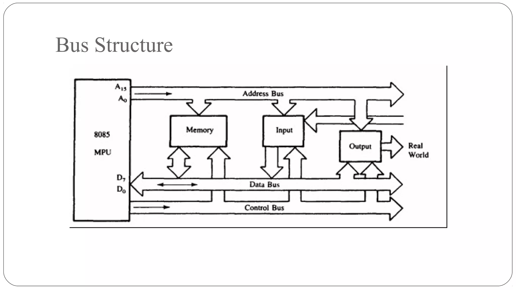
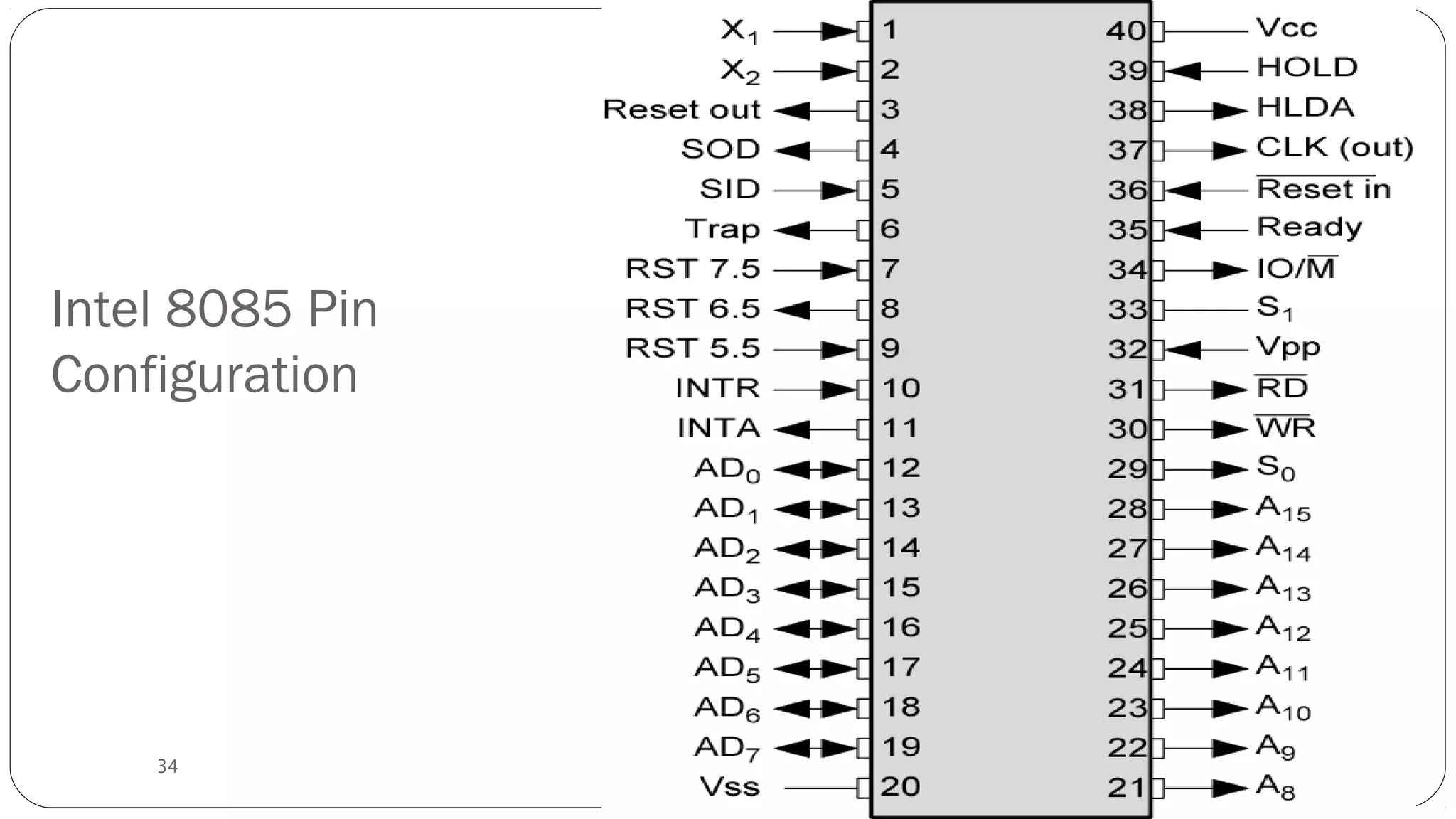
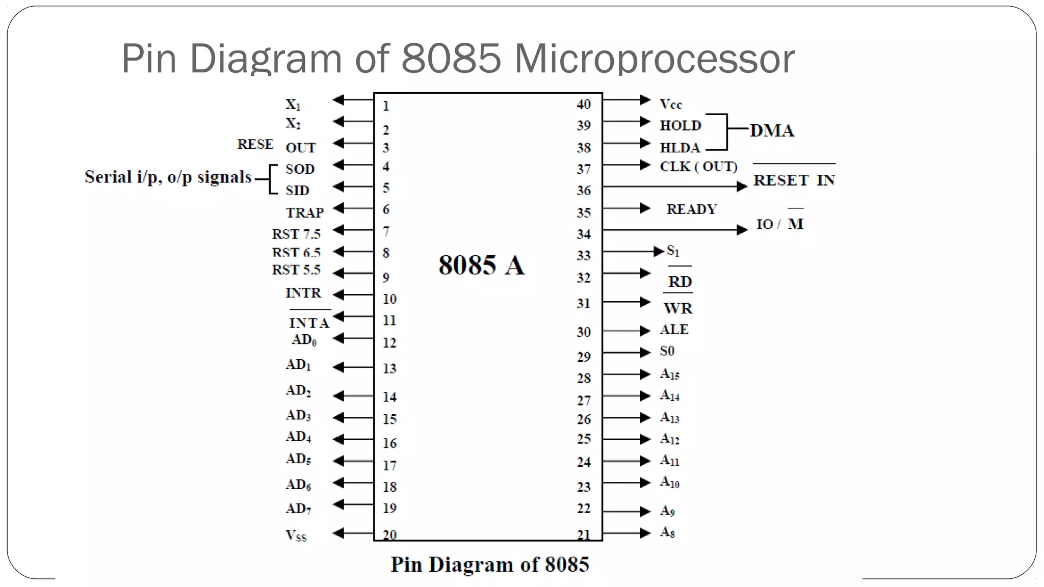
SlideShare a Scribd company logo
8085 Microprocessor
8085 ARCHITECTURE
8085 BUS ORGANIZATION AND STRUCTURE
8085 PIN FUNCTIONS
History of microprocessor
Intel's 4004 is considered the first microprocesor .
The 4004 was later followed in 1972 by the 8008, the
world's first 8-bit microprocessor.
History of microprocessor……
Then is the 8080 microprocessor evolved in
1974.
Then comes 8085 that is the 8 bit
microprocessor
Microprocessor 8085
• The 8085 is an 8-bit general purpose microprocessor that can address
64K Byte of memory.
• It has 40 pins and uses +5V for power. It can run at a maximum
frequency of 3 MHz
• The pins on the chip can be grouped into 6 groups:
• Address Bus.
• Data Bus.
• Control and Status Signals.
• Power supply and frequency.
• Externally Initiated Signals.
• Serial I/O ports.
8085 ARCHITECTURE BLOCK DIAGRAM
Register Section
• Temporary Register
• General Purpose Register
• Special Purpose Registers
Temporary Registers
• In 8085 available temporary register are temporary data register and
W and Z registers. These registers are not available to the
programmer, but 8085 uses them internally to hold temporary data
during execution of some instructions.
• W and Z are two 8-bit temporary registers, used to hold 8-bit
data/address during execution of some instructions.
General Purpose RegistersB,C,D,E,H &L are used as general purpose register.
Each 8 bit long .
Apart from the above function these registers can also be used to
work in pairs to hold 16-bit data.
They can work in pairs such as B-C, D-E and H-L to store 16-bit
data.
The H-L pair works as a memory pointer.
A memory pointer holds the address of a particular memory location.
They can store 16-bit address as they work in pair.
Special Purpose Register
• Accumulator
• Status or Flag Register
• Instruction Register
• Program Counter
• Stack Pointer
Accumulator
• The accumulator is an 8-bit register that is a part of
arithmetic/logic unit (ALU).
• This register is used to store 8-bit data and to perform
arithmetic and logical operations.
• The result of an operation is stored in the accumulator.
The accumulator is also identified as register A.
• It also works as a via register for I/O accesses i.e. it
reads data from input device and similarly can transfer
data to output device.
Status or Flag Register
Flag register is a group of flip flops used to give status of different
operations result.
The flag register is connected to ALU.
Once an operation is performed by ALU the result is transferred on
internal data bus and status of result will be stored in flip flops.
They are called Zero (Z), Carry (CY), Sign (S), Parity (P), and
Auxiliary Carry (AC) flags.
Flag Register…
• A flag register contains a number of flags either to
indicate certain conditions arising after arithmetic and
logical operations or to control certain operations.
• The flags which indicate conditions are known as
condition flags. The flags which are used to control
certain operations are called control flags.
• A flag is a flip-flop which is set or reset by the
processor to indicate certain conditions or set/reset by
the programmer to control certain operations.
Flag Register… Carry flag(CY):
 If an operation performed in ALU generates the carry from D7 to next stage then CY flag is set,
else it is reset.
 Auxiliary carry(AC):
 If an operation performed in ALU generates the carry from lower nibble (D0 to D3) to upper
nibble (D4 to D7) AC flag is set, else it resets.
 Zero flag(z):
 If an operation performed in ALU results 0value of entire 8-bits then zero flag is set, else it resets
 Sign flag(s):
 If MSB bit =0 then the number is positive, else it is negative.
 Parity flag(p):
 If the result contains even no. of ones this flag is set and for odd no. of ones this flag is reset.
Instruction Register
Temporary store for the current instruction of a program. Latest instruction sent here
from memory prior to execution. Decoder then takes instruction and decodes or
interprets the instruction. Decoded instruction then passed to next stage.
Instruction register is 8-bit register just like every other register of
microprocessor. Consider an instruction. The instruction may be anything like adding
two data's, moving a data, copying a data etc. When such an instruction is fetched from
memory, it is directed to Instruction register. So the instruction registers are specifically
to store the instructions that are fetched from memory.
There is an Instruction decoder which decodes the information's present in the
Instruction register for further processing.
Program Counter
• This 16-bit register deals with sequencing the execution of
instructions. This register is a memory pointer. Memory
locations have 16-bit addresses, and that is why this is a
16-bit register.
• The microprocessor uses this register to sequence the
execution of the instructions. The function of the program counter
is to point to the memory address from which the next byte is to be
fetched. When a byte is being fetched, the program counter is
incremented by one to point to the next memory location
Stack Pointer
• The stack pointer is also a 16-bit register used as a memory pointer. It points to a
memory location in R/W memory, called the stack. The beginning of the stack is
defined by loading 16-bit address in the stack pointer.
• Stack pointer is also a 16-bit register which is used as a memory pointer.
• A stack is nothing but the portion of RAM (Random access memory).
• Stack pointer maintains the address of the last byte that is entered into stack.
• Each time when the data is loaded into stack, Stack pointer gets decremented.
• Conversely it is incremented when data is retrieved from stack
ALU
• The ALU performs the actual numerical and logic operation such as add,
subtract, AND, OR, etc. Uses data from memory and from Accumulator to
perform arithmetic. Always stores result of operation in Accumulator.
• It is not accessible by user.
• The word length of ALU depends upon of an internal data bus.
• IT is 8 bit. It is always controlled by timing and control circuits.
• It provides status or result of flag register.
Arithmetic and Logical Section
• Instruction Decoder and Machine cycle Encoder
• Address Buffer
• Address/Data Buffer
• Incrementer/Decrementer Address Latch
• Interrupt Control
• Serial I/O Control Group
• Timing And Control
Instruction Decoder and Machine cycle Encoder
• It accepts an OPCODE from instruction register, decodes it and
gives
the decoded information to control logic.
• The information includes what operation is to be performed, who is
going to perform it, etc. It means it will understand the instruction
in
this block.
• The decoded information is given to the timing and control unit that
provides control signals
Address Buffer
• The contents of the stack pointer and program counter are loaded into the
address buffer and address-data buffer.
• These buffers are then used to drive the external address bus and address-data
bus.
• As the memory and I/O chips are connected to these buses, the CPU can
exchange desired data to the memory and I/O chips.
• The address-data buffer is not only connected to the external data bus but also to
the internal data bus which consists of 8-bits.
• The address data buffer can both send and receive data from internal data bus.
• The contents of the stack pointer and program counter are loaded into the
address buffer and address-data buffer. These buffers are then used to
drive the external address bus and address-data bus. As the memory and I/O
chips are connected to these buses, the CPU can exchange desired data to
the memory and I/O chips.
• The address-data buffer is not only connected to the external data bus but also to
the internal data bus which consists of 8-bits. The address data buffer can
both send and receive data from internal data bus.
Incrementer/Decrementer Address Latch
• The 8-bit contents of a register or a memory location
can be incremented or decremented by 1.
• This 16-bit register is used to increment or
decrement the content of program counter and
stack pointer register by 1.
• Increment or decrement can be performed on any
register or a memory location.
Interrupt Control
• Consider that a microprocessor is executing the main program.
Now whenever the interrupt signal is enabled or requested the
microprocessor shifts the control from main program to process
the incoming request and after the completion of request, the
control goes back to the main program.
• For example an Input/output device may send an interrupt signal
to notify that the data is ready for input. The microprocessor
temporarily stops the execution of main program and transfers
control to I/O device. After collecting the input data the control
is transferred back to main program.
Serial I/O Control Group
• The data transferred on to data bus is parallel data,
but under some conditions it is advantageous to use
serial data transfer at that time this control group is
brought into application.
• The input and output of serial data can be carried
out using 2 instructions in 8085:
• 1. SID-Serial Input Data
• 2. SOD-Serial Output Data
Timing And Control
Timing and control unit is a very important unit as it synchronizes the registers
and flow of data through various registers and other units.
It accepts data from instruction decoder and generates micro steps to perform it
,in addition it accepts clock inputs for synchronizing operations.
This unit consists of an oscillator and controller sequencer which sends control
signals needed for internal and external control of data and other units.
1. Control Signals: READY, RD(bar), WR(bar), ALE
2. Status Signals: S0, S1, IO/M(bar)
3. DMA Signals: HOLD, HLDA
4. RESET Signals: RESET IN(bar), RESET OUT.
Bus Organization
• What is a Bus?
• It is a set of pins, wires or signals having common
functions as bus.
• What is system Bus?
• A bus is a bundle of wires that are grouped together to
serve a single purpose in microprocessor, generally there
are three sets of communication lines that are called
buses.
• They are address bus, the data bus and control bus.
Bus Structure
Address Bus
• The bus over which the microprocessor sends out the address
of a memory location or I/O location is called as the address
bus.
• In 8085 microprocessor, Address bus is of 16 bits. This means
that Microprocessor 8085 can transfer maximum 16 bit address
which means it can address 65,536 different memory locations.
• This bus is multiplexed with 8 bit data bus. So, the most
significant bits (MSB) of address goes through Address bus
and LSB goes through multiplexed data bus.
• In 8085 address bus is 16 bit A0 – A15
Data Bus
• It is bi-directional as Microprocessor requires to send or
receiver data. The data bus also works as bus in 8 bits long.
• A data bus simply carries data. Internal buses carry information
within the processor, while external buses carry data between
the processor and the memory. Typically, the same data bus is
used for both read/write operations.
• When it is a write operation, the processor will put the data on
to the data bus. When it is the read operation, the memory
controller will get the data from the specific memory block and
put it in to the data bus.
• The data bus in8085 is of 8 parallel lines D0 – D7
Control Bus
• The control bus is used for sending control signals to the
memory and I/O devices. The CPU sends control signal
on the control bus to enable the outputs of addressed
memory devices or I/O port devices.
• Some of the control bus signals are as follows:
• 1.Memory read
• 2.Memory write
• 3.I/O read
• 4.I/O write.
33 Signals and I/O Pins
34
Intel 8085 Pin
Configuration
Pin Diagram of 8085 Microprocessor
• Power Supply Signal and clock signal:
• VCC :- Vcc is to be connected to +5V power supply.
• Vss :- Ground reference
• X1 and X2:-
• This pin is used for providing the clock frequency to the
microprocessor. Generally Crystal oscillator or LC
oscillator is used to generate the frequency. The frequency
generated here is internally divided into two. As we know
that the basic operating timing frequency of the
microprocessor is 3 MHz so 6 MHz frequency is applied.
• Address Bus:
• A8 - A15: (output; 3-state)
• It carries the most significant 8 bits of the memory address or the 8 bits
of the I/O address.
• Data bus:
• AD0 - AD7 (input/output; 3-state)
• These multiplexed set of lines used to carry the lower order 8 bit
address as well as data bus.
• During the opcode fetch operation, in the first clock cycle, the lines
deliver the lower order address A0 - A7.
• In the subsequent IO / memory, read / write clock cycle the lines are
used as data bus.
• The CPU may read or write out data through these lines.
Control and Status signals:
• ALE (output) - Address Latch Enable.
• It is an output signal used to give information of AD0-
AD7 contents.
• It is a positive going pulse generated when a new
operation is started by microprocessor.
• When pulse goes high it indicates that AD0-AD7 are
address.
• When it is low it indicates that the contents are data.
• RD (output 3-state, active low)
• Read memory or IO device.
• This indicates that the selected memory location or
I/O device is to be read and that the data bus is ready
for accepting data from the memory or I/O device
• WR (output 3-state, active low)
• Write memory or IO device.
• This indicates that the data on the data bus is to be
written into the selected memory location or I/O
device.
• I/O M (output)
• Select memory or an IO device.
• This status signal indicates that the read / write
operation relates to whether the memory or I/O
device.
• It goes high to indicate an I/O operation.
• It goes low for memory operations.
Interrupts and Externally initiated operations:
• They are the signals initiated by an external device
to request the microprocessor to do a
particular task or work.
• There are five hardware interrupts called,
• TRAP
• RST 7.5
• RST 6.5
• RST 5.5
• INTA
• Reset In (input, active low)
• This signal is used to reset the microprocessor.
• The program counter inside the microprocessor is
set to zero.
• The buses are tri-stated.
• Reset Out (Output)
• It indicates CPU is being reset.
• Used to reset all the connected devices when the
microprocessor is reset.
References
• A course on 8085 Microprocessor –
Prentice Hall
• Microprocessor 8085 by Ramesh Gaonkar
Mp 8085
Mp 8085

More Related Content

What's hot

Stack in 8085 microprocessor
Stack in 8085 microprocessorStack in 8085 microprocessor
Stack in 8085 microprocessor
hepzijustin
 
8051 Microcontroller PPT's By Er. Swapnil Kaware
8051 Microcontroller PPT's By Er. Swapnil Kaware8051 Microcontroller PPT's By Er. Swapnil Kaware
8051 Microcontroller PPT's By Er. Swapnil KawareProf. Swapnil V. Kaware
 
Addressing modes 8085
Addressing modes 8085Addressing modes 8085
Addressing modes 8085
ShivamSood22
 
Introduction to 8085 microprocessor
Introduction to 8085 microprocessorIntroduction to 8085 microprocessor
Introduction to 8085 microprocessor
venkateshkannat
 
Timing diagram 8085 microprocessor
Timing diagram 8085 microprocessorTiming diagram 8085 microprocessor
Timing diagram 8085 microprocessor
Velalar College of Engineering and Technology
 
8257 DMA Controller
8257 DMA Controller8257 DMA Controller
8257 DMA Controller
ShivamSood22
 
System bus timing 8086
System bus timing 8086System bus timing 8086
System bus timing 8086
mpsrekha83
 
Chapter 1 microprocessor introduction
Chapter 1 microprocessor introductionChapter 1 microprocessor introduction
Chapter 1 microprocessor introduction
Shubham Singh
 
Architecture of 8051
Architecture of 8051Architecture of 8051
Architecture of 8051
hello_priti
 
Instruction set of 8085
Instruction set of 8085Instruction set of 8085
microprocessor
 microprocessor microprocessor
microprocessor
ATTO RATHORE
 
Minimum Modes and Maximum Modes of 8086 Microprocessor
Minimum Modes and Maximum Modes of 8086 MicroprocessorMinimum Modes and Maximum Modes of 8086 Microprocessor
Minimum Modes and Maximum Modes of 8086 MicroprocessorNikhil Kumar
 
PPT on 8085 Microprocessor
PPT on 8085 Microprocessor  PPT on 8085 Microprocessor
PPT on 8085 Microprocessor
DebrajJana4
 
8085 MICROPROCESSOR ARCHITECTURE AND ITS OPERATIONS
8085 MICROPROCESSOR ARCHITECTURE AND ITS OPERATIONS8085 MICROPROCESSOR ARCHITECTURE AND ITS OPERATIONS
8085 MICROPROCESSOR ARCHITECTURE AND ITS OPERATIONS
RamaPrabha24
 
Microprocessor 8086
Microprocessor 8086Microprocessor 8086
Microprocessor 8086
Gopikrishna Madanan
 
8259 Interrupt Controller
8259 Interrupt Controller8259 Interrupt Controller
8259 Interrupt Controller
ShivamSood22
 
Microprocessor 8085 complete
Microprocessor 8085 completeMicroprocessor 8085 complete
Microprocessor 8085 complete
Shubham Singh
 
8086 micro processor
8086 micro processor8086 micro processor
8086 micro processor
Poojith Chowdhary
 
Interrupts in 8051
Interrupts in 8051Interrupts in 8051
Interrupts in 8051
Sudhanshu Janwadkar
 

What's hot (20)

Stack in 8085 microprocessor
Stack in 8085 microprocessorStack in 8085 microprocessor
Stack in 8085 microprocessor
 
8051 Microcontroller PPT's By Er. Swapnil Kaware
8051 Microcontroller PPT's By Er. Swapnil Kaware8051 Microcontroller PPT's By Er. Swapnil Kaware
8051 Microcontroller PPT's By Er. Swapnil Kaware
 
Addressing modes 8085
Addressing modes 8085Addressing modes 8085
Addressing modes 8085
 
Introduction to 8085 microprocessor
Introduction to 8085 microprocessorIntroduction to 8085 microprocessor
Introduction to 8085 microprocessor
 
Timing diagram 8085 microprocessor
Timing diagram 8085 microprocessorTiming diagram 8085 microprocessor
Timing diagram 8085 microprocessor
 
8257 DMA Controller
8257 DMA Controller8257 DMA Controller
8257 DMA Controller
 
System bus timing 8086
System bus timing 8086System bus timing 8086
System bus timing 8086
 
Chapter 1 microprocessor introduction
Chapter 1 microprocessor introductionChapter 1 microprocessor introduction
Chapter 1 microprocessor introduction
 
Architecture of 8051
Architecture of 8051Architecture of 8051
Architecture of 8051
 
Instruction set of 8085
Instruction set of 8085Instruction set of 8085
Instruction set of 8085
 
microprocessor
 microprocessor microprocessor
microprocessor
 
Minimum Modes and Maximum Modes of 8086 Microprocessor
Minimum Modes and Maximum Modes of 8086 MicroprocessorMinimum Modes and Maximum Modes of 8086 Microprocessor
Minimum Modes and Maximum Modes of 8086 Microprocessor
 
PPT on 8085 Microprocessor
PPT on 8085 Microprocessor  PPT on 8085 Microprocessor
PPT on 8085 Microprocessor
 
8085 MICROPROCESSOR ARCHITECTURE AND ITS OPERATIONS
8085 MICROPROCESSOR ARCHITECTURE AND ITS OPERATIONS8085 MICROPROCESSOR ARCHITECTURE AND ITS OPERATIONS
8085 MICROPROCESSOR ARCHITECTURE AND ITS OPERATIONS
 
Microprocessor 8086
Microprocessor 8086Microprocessor 8086
Microprocessor 8086
 
8259 Interrupt Controller
8259 Interrupt Controller8259 Interrupt Controller
8259 Interrupt Controller
 
Microprocessor 8085 complete
Microprocessor 8085 completeMicroprocessor 8085 complete
Microprocessor 8085 complete
 
Interfacing 8255
Interfacing 8255Interfacing 8255
Interfacing 8255
 
8086 micro processor
8086 micro processor8086 micro processor
8086 micro processor
 
Interrupts in 8051
Interrupts in 8051Interrupts in 8051
Interrupts in 8051
 

Similar to Mp 8085

8085 microprocessor architecture
8085 microprocessor architecture8085 microprocessor architecture
8085 microprocessor architecture
Arashdeepkaur16
 
8085-microprocessor
8085-microprocessor8085-microprocessor
8085-microprocessor
ATTO RATHORE
 
8085 architecture
8085 architecture8085 architecture
8085 architecture
kunwer brijendra shanker
 
MPMC
MPMC MPMC
8085 microprocessor
8085 microprocessor8085 microprocessor
8085 microprocessor
GurleenKaur408
 
lec3-8051microcontrollerarchitecture-230130044236-5c11a082.pptx
lec3-8051microcontrollerarchitecture-230130044236-5c11a082.pptxlec3-8051microcontrollerarchitecture-230130044236-5c11a082.pptx
lec3-8051microcontrollerarchitecture-230130044236-5c11a082.pptx
MadavanR1
 
MP_MC.pdf
MP_MC.pdfMP_MC.pdf
MP_MC.pdf
KRamasamy2
 
8051 MICROCONTROLLER ARCHITECTURE.pptx
 8051 MICROCONTROLLER ARCHITECTURE.pptx 8051 MICROCONTROLLER ARCHITECTURE.pptx
8051 MICROCONTROLLER ARCHITECTURE.pptx
MemonaMemon1
 
UNIT 1 Microprocessors.pptx
UNIT 1 Microprocessors.pptxUNIT 1 Microprocessors.pptx
UNIT 1 Microprocessors.pptx
Gowrishankar C
 
Architecture of 8085
Architecture of 8085Architecture of 8085
Architecture of 8085
HarshitParkar6677
 
Architecture of 8085
Architecture of 8085Architecture of 8085
Architecture of 8085
HarshitParkar6677
 
Microprocessors 8085 architecture
Microprocessors 8085 architectureMicroprocessors 8085 architecture
Microprocessors 8085 architecture
VARUN BABUNELSON
 
itft-8085 microprocessor
itft-8085 microprocessoritft-8085 microprocessor
itft-8085 microprocessorShifali Sharma
 
Mechatronics UNIT 2.pptx
Mechatronics UNIT 2.pptxMechatronics UNIT 2.pptx
Mechatronics UNIT 2.pptx
ssuser823c58
 
Microprocessors and microcontrollers
Microprocessors and microcontrollersMicroprocessors and microcontrollers
Microprocessors and microcontrollers
gomathy S
 
architect.ppt
architect.pptarchitect.ppt
architect.ppt
SELVAPRIYAA2
 
Microprocessor and Microcontroller lec2
Microprocessor and Microcontroller lec2Microprocessor and Microcontroller lec2
Microprocessor and Microcontroller lec2
Ameen San
 
Ree602 microprocessor unit ii
Ree602  microprocessor unit iiRee602  microprocessor unit ii
Ree602 microprocessor unit ii
MAHMOOD ilahi
 

Similar to Mp 8085 (20)

8085 microprocessor architecture
8085 microprocessor architecture8085 microprocessor architecture
8085 microprocessor architecture
 
12 mt06ped001
12 mt06ped001 12 mt06ped001
12 mt06ped001
 
8085-microprocessor
8085-microprocessor8085-microprocessor
8085-microprocessor
 
8085 architecture
8085 architecture8085 architecture
8085 architecture
 
MPMC
MPMC MPMC
MPMC
 
c++
c++ c++
c++
 
8085 microprocessor
8085 microprocessor8085 microprocessor
8085 microprocessor
 
lec3-8051microcontrollerarchitecture-230130044236-5c11a082.pptx
lec3-8051microcontrollerarchitecture-230130044236-5c11a082.pptxlec3-8051microcontrollerarchitecture-230130044236-5c11a082.pptx
lec3-8051microcontrollerarchitecture-230130044236-5c11a082.pptx
 
MP_MC.pdf
MP_MC.pdfMP_MC.pdf
MP_MC.pdf
 
8051 MICROCONTROLLER ARCHITECTURE.pptx
 8051 MICROCONTROLLER ARCHITECTURE.pptx 8051 MICROCONTROLLER ARCHITECTURE.pptx
8051 MICROCONTROLLER ARCHITECTURE.pptx
 
UNIT 1 Microprocessors.pptx
UNIT 1 Microprocessors.pptxUNIT 1 Microprocessors.pptx
UNIT 1 Microprocessors.pptx
 
Architecture of 8085
Architecture of 8085Architecture of 8085
Architecture of 8085
 
Architecture of 8085
Architecture of 8085Architecture of 8085
Architecture of 8085
 
Microprocessors 8085 architecture
Microprocessors 8085 architectureMicroprocessors 8085 architecture
Microprocessors 8085 architecture
 
itft-8085 microprocessor
itft-8085 microprocessoritft-8085 microprocessor
itft-8085 microprocessor
 
Mechatronics UNIT 2.pptx
Mechatronics UNIT 2.pptxMechatronics UNIT 2.pptx
Mechatronics UNIT 2.pptx
 
Microprocessors and microcontrollers
Microprocessors and microcontrollersMicroprocessors and microcontrollers
Microprocessors and microcontrollers
 
architect.ppt
architect.pptarchitect.ppt
architect.ppt
 
Microprocessor and Microcontroller lec2
Microprocessor and Microcontroller lec2Microprocessor and Microcontroller lec2
Microprocessor and Microcontroller lec2
 
Ree602 microprocessor unit ii
Ree602  microprocessor unit iiRee602  microprocessor unit ii
Ree602 microprocessor unit ii
 

Recently uploaded

Nuclear Power Economics and Structuring 2024
Nuclear Power Economics and Structuring 2024Nuclear Power Economics and Structuring 2024
Nuclear Power Economics and Structuring 2024
Massimo Talia
 
Planning Of Procurement o different goods and services
Planning Of Procurement o different goods and servicesPlanning Of Procurement o different goods and services
Planning Of Procurement o different goods and services
JoytuBarua2
 
LIGA(E)11111111111111111111111111111111111111111.ppt
LIGA(E)11111111111111111111111111111111111111111.pptLIGA(E)11111111111111111111111111111111111111111.ppt
LIGA(E)11111111111111111111111111111111111111111.ppt
ssuser9bd3ba
 
ethical hacking in wireless-hacking1.ppt
ethical hacking in wireless-hacking1.pptethical hacking in wireless-hacking1.ppt
ethical hacking in wireless-hacking1.ppt
Jayaprasanna4
 
Courier management system project report.pdf
Courier management system project report.pdfCourier management system project report.pdf
Courier management system project report.pdf
Kamal Acharya
 
HYDROPOWER - Hydroelectric power generation
HYDROPOWER - Hydroelectric power generationHYDROPOWER - Hydroelectric power generation
HYDROPOWER - Hydroelectric power generation
Robbie Edward Sayers
 
Halogenation process of chemical process industries
Halogenation process of chemical process industriesHalogenation process of chemical process industries
Halogenation process of chemical process industries
MuhammadTufail242431
 
WATER CRISIS and its solutions-pptx 1234
WATER CRISIS and its solutions-pptx 1234WATER CRISIS and its solutions-pptx 1234
WATER CRISIS and its solutions-pptx 1234
AafreenAbuthahir2
 
Automobile Management System Project Report.pdf
Automobile Management System Project Report.pdfAutomobile Management System Project Report.pdf
Automobile Management System Project Report.pdf
Kamal Acharya
 
weather web application report.pdf
weather web application report.pdfweather web application report.pdf
weather web application report.pdf
Pratik Pawar
 
addressing modes in computer architecture
addressing modes  in computer architectureaddressing modes  in computer architecture
addressing modes in computer architecture
ShahidSultan24
 
COLLEGE BUS MANAGEMENT SYSTEM PROJECT REPORT.pdf
COLLEGE BUS MANAGEMENT SYSTEM PROJECT REPORT.pdfCOLLEGE BUS MANAGEMENT SYSTEM PROJECT REPORT.pdf
COLLEGE BUS MANAGEMENT SYSTEM PROJECT REPORT.pdf
Kamal Acharya
 
TECHNICAL TRAINING MANUAL GENERAL FAMILIARIZATION COURSE
TECHNICAL TRAINING MANUAL   GENERAL FAMILIARIZATION COURSETECHNICAL TRAINING MANUAL   GENERAL FAMILIARIZATION COURSE
TECHNICAL TRAINING MANUAL GENERAL FAMILIARIZATION COURSE
DuvanRamosGarzon1
 
Cosmetic shop management system project report.pdf
Cosmetic shop management system project report.pdfCosmetic shop management system project report.pdf
Cosmetic shop management system project report.pdf
Kamal Acharya
 
Water Industry Process Automation and Control Monthly - May 2024.pdf
Water Industry Process Automation and Control Monthly - May 2024.pdfWater Industry Process Automation and Control Monthly - May 2024.pdf
Water Industry Process Automation and Control Monthly - May 2024.pdf
Water Industry Process Automation & Control
 
Event Management System Vb Net Project Report.pdf
Event Management System Vb Net  Project Report.pdfEvent Management System Vb Net  Project Report.pdf
Event Management System Vb Net Project Report.pdf
Kamal Acharya
 
Pile Foundation by Venkatesh Taduvai (Sub Geotechnical Engineering II)-conver...
Pile Foundation by Venkatesh Taduvai (Sub Geotechnical Engineering II)-conver...Pile Foundation by Venkatesh Taduvai (Sub Geotechnical Engineering II)-conver...
Pile Foundation by Venkatesh Taduvai (Sub Geotechnical Engineering II)-conver...
AJAYKUMARPUND1
 
Architectural Portfolio Sean Lockwood
Architectural Portfolio Sean LockwoodArchitectural Portfolio Sean Lockwood
Architectural Portfolio Sean Lockwood
seandesed
 
ethical hacking-mobile hacking methods.ppt
ethical hacking-mobile hacking methods.pptethical hacking-mobile hacking methods.ppt
ethical hacking-mobile hacking methods.ppt
Jayaprasanna4
 
Vaccine management system project report documentation..pdf
Vaccine management system project report documentation..pdfVaccine management system project report documentation..pdf
Vaccine management system project report documentation..pdf
Kamal Acharya
 

Recently uploaded (20)

Nuclear Power Economics and Structuring 2024
Nuclear Power Economics and Structuring 2024Nuclear Power Economics and Structuring 2024
Nuclear Power Economics and Structuring 2024
 
Planning Of Procurement o different goods and services
Planning Of Procurement o different goods and servicesPlanning Of Procurement o different goods and services
Planning Of Procurement o different goods and services
 
LIGA(E)11111111111111111111111111111111111111111.ppt
LIGA(E)11111111111111111111111111111111111111111.pptLIGA(E)11111111111111111111111111111111111111111.ppt
LIGA(E)11111111111111111111111111111111111111111.ppt
 
ethical hacking in wireless-hacking1.ppt
ethical hacking in wireless-hacking1.pptethical hacking in wireless-hacking1.ppt
ethical hacking in wireless-hacking1.ppt
 
Courier management system project report.pdf
Courier management system project report.pdfCourier management system project report.pdf
Courier management system project report.pdf
 
HYDROPOWER - Hydroelectric power generation
HYDROPOWER - Hydroelectric power generationHYDROPOWER - Hydroelectric power generation
HYDROPOWER - Hydroelectric power generation
 
Halogenation process of chemical process industries
Halogenation process of chemical process industriesHalogenation process of chemical process industries
Halogenation process of chemical process industries
 
WATER CRISIS and its solutions-pptx 1234
WATER CRISIS and its solutions-pptx 1234WATER CRISIS and its solutions-pptx 1234
WATER CRISIS and its solutions-pptx 1234
 
Automobile Management System Project Report.pdf
Automobile Management System Project Report.pdfAutomobile Management System Project Report.pdf
Automobile Management System Project Report.pdf
 
weather web application report.pdf
weather web application report.pdfweather web application report.pdf
weather web application report.pdf
 
addressing modes in computer architecture
addressing modes  in computer architectureaddressing modes  in computer architecture
addressing modes in computer architecture
 
COLLEGE BUS MANAGEMENT SYSTEM PROJECT REPORT.pdf
COLLEGE BUS MANAGEMENT SYSTEM PROJECT REPORT.pdfCOLLEGE BUS MANAGEMENT SYSTEM PROJECT REPORT.pdf
COLLEGE BUS MANAGEMENT SYSTEM PROJECT REPORT.pdf
 
TECHNICAL TRAINING MANUAL GENERAL FAMILIARIZATION COURSE
TECHNICAL TRAINING MANUAL   GENERAL FAMILIARIZATION COURSETECHNICAL TRAINING MANUAL   GENERAL FAMILIARIZATION COURSE
TECHNICAL TRAINING MANUAL GENERAL FAMILIARIZATION COURSE
 
Cosmetic shop management system project report.pdf
Cosmetic shop management system project report.pdfCosmetic shop management system project report.pdf
Cosmetic shop management system project report.pdf
 
Water Industry Process Automation and Control Monthly - May 2024.pdf
Water Industry Process Automation and Control Monthly - May 2024.pdfWater Industry Process Automation and Control Monthly - May 2024.pdf
Water Industry Process Automation and Control Monthly - May 2024.pdf
 
Event Management System Vb Net Project Report.pdf
Event Management System Vb Net  Project Report.pdfEvent Management System Vb Net  Project Report.pdf
Event Management System Vb Net Project Report.pdf
 
Pile Foundation by Venkatesh Taduvai (Sub Geotechnical Engineering II)-conver...
Pile Foundation by Venkatesh Taduvai (Sub Geotechnical Engineering II)-conver...Pile Foundation by Venkatesh Taduvai (Sub Geotechnical Engineering II)-conver...
Pile Foundation by Venkatesh Taduvai (Sub Geotechnical Engineering II)-conver...
 
Architectural Portfolio Sean Lockwood
Architectural Portfolio Sean LockwoodArchitectural Portfolio Sean Lockwood
Architectural Portfolio Sean Lockwood
 
ethical hacking-mobile hacking methods.ppt
ethical hacking-mobile hacking methods.pptethical hacking-mobile hacking methods.ppt
ethical hacking-mobile hacking methods.ppt
 
Vaccine management system project report documentation..pdf
Vaccine management system project report documentation..pdfVaccine management system project report documentation..pdf
Vaccine management system project report documentation..pdf
 

Mp 8085

  • 2. 8085 ARCHITECTURE 8085 BUS ORGANIZATION AND STRUCTURE 8085 PIN FUNCTIONS
  • 3. History of microprocessor Intel's 4004 is considered the first microprocesor . The 4004 was later followed in 1972 by the 8008, the world's first 8-bit microprocessor.
  • 4. History of microprocessor…… Then is the 8080 microprocessor evolved in 1974. Then comes 8085 that is the 8 bit microprocessor
  • 5. Microprocessor 8085 • The 8085 is an 8-bit general purpose microprocessor that can address 64K Byte of memory. • It has 40 pins and uses +5V for power. It can run at a maximum frequency of 3 MHz • The pins on the chip can be grouped into 6 groups: • Address Bus. • Data Bus. • Control and Status Signals. • Power supply and frequency. • Externally Initiated Signals. • Serial I/O ports.
  • 7.
  • 8. Register Section • Temporary Register • General Purpose Register • Special Purpose Registers
  • 9. Temporary Registers • In 8085 available temporary register are temporary data register and W and Z registers. These registers are not available to the programmer, but 8085 uses them internally to hold temporary data during execution of some instructions. • W and Z are two 8-bit temporary registers, used to hold 8-bit data/address during execution of some instructions.
  • 10. General Purpose RegistersB,C,D,E,H &L are used as general purpose register. Each 8 bit long . Apart from the above function these registers can also be used to work in pairs to hold 16-bit data. They can work in pairs such as B-C, D-E and H-L to store 16-bit data. The H-L pair works as a memory pointer. A memory pointer holds the address of a particular memory location. They can store 16-bit address as they work in pair.
  • 11. Special Purpose Register • Accumulator • Status or Flag Register • Instruction Register • Program Counter • Stack Pointer
  • 12. Accumulator • The accumulator is an 8-bit register that is a part of arithmetic/logic unit (ALU). • This register is used to store 8-bit data and to perform arithmetic and logical operations. • The result of an operation is stored in the accumulator. The accumulator is also identified as register A. • It also works as a via register for I/O accesses i.e. it reads data from input device and similarly can transfer data to output device.
  • 13. Status or Flag Register Flag register is a group of flip flops used to give status of different operations result. The flag register is connected to ALU. Once an operation is performed by ALU the result is transferred on internal data bus and status of result will be stored in flip flops. They are called Zero (Z), Carry (CY), Sign (S), Parity (P), and Auxiliary Carry (AC) flags.
  • 14. Flag Register… • A flag register contains a number of flags either to indicate certain conditions arising after arithmetic and logical operations or to control certain operations. • The flags which indicate conditions are known as condition flags. The flags which are used to control certain operations are called control flags. • A flag is a flip-flop which is set or reset by the processor to indicate certain conditions or set/reset by the programmer to control certain operations.
  • 15. Flag Register… Carry flag(CY):  If an operation performed in ALU generates the carry from D7 to next stage then CY flag is set, else it is reset.  Auxiliary carry(AC):  If an operation performed in ALU generates the carry from lower nibble (D0 to D3) to upper nibble (D4 to D7) AC flag is set, else it resets.  Zero flag(z):  If an operation performed in ALU results 0value of entire 8-bits then zero flag is set, else it resets  Sign flag(s):  If MSB bit =0 then the number is positive, else it is negative.  Parity flag(p):  If the result contains even no. of ones this flag is set and for odd no. of ones this flag is reset.
  • 16. Instruction Register Temporary store for the current instruction of a program. Latest instruction sent here from memory prior to execution. Decoder then takes instruction and decodes or interprets the instruction. Decoded instruction then passed to next stage. Instruction register is 8-bit register just like every other register of microprocessor. Consider an instruction. The instruction may be anything like adding two data's, moving a data, copying a data etc. When such an instruction is fetched from memory, it is directed to Instruction register. So the instruction registers are specifically to store the instructions that are fetched from memory. There is an Instruction decoder which decodes the information's present in the Instruction register for further processing.
  • 17. Program Counter • This 16-bit register deals with sequencing the execution of instructions. This register is a memory pointer. Memory locations have 16-bit addresses, and that is why this is a 16-bit register. • The microprocessor uses this register to sequence the execution of the instructions. The function of the program counter is to point to the memory address from which the next byte is to be fetched. When a byte is being fetched, the program counter is incremented by one to point to the next memory location
  • 18. Stack Pointer • The stack pointer is also a 16-bit register used as a memory pointer. It points to a memory location in R/W memory, called the stack. The beginning of the stack is defined by loading 16-bit address in the stack pointer. • Stack pointer is also a 16-bit register which is used as a memory pointer. • A stack is nothing but the portion of RAM (Random access memory). • Stack pointer maintains the address of the last byte that is entered into stack. • Each time when the data is loaded into stack, Stack pointer gets decremented. • Conversely it is incremented when data is retrieved from stack
  • 19. ALU • The ALU performs the actual numerical and logic operation such as add, subtract, AND, OR, etc. Uses data from memory and from Accumulator to perform arithmetic. Always stores result of operation in Accumulator. • It is not accessible by user. • The word length of ALU depends upon of an internal data bus. • IT is 8 bit. It is always controlled by timing and control circuits. • It provides status or result of flag register.
  • 20. Arithmetic and Logical Section • Instruction Decoder and Machine cycle Encoder • Address Buffer • Address/Data Buffer • Incrementer/Decrementer Address Latch • Interrupt Control • Serial I/O Control Group • Timing And Control
  • 21. Instruction Decoder and Machine cycle Encoder • It accepts an OPCODE from instruction register, decodes it and gives the decoded information to control logic. • The information includes what operation is to be performed, who is going to perform it, etc. It means it will understand the instruction in this block. • The decoded information is given to the timing and control unit that provides control signals
  • 22. Address Buffer • The contents of the stack pointer and program counter are loaded into the address buffer and address-data buffer. • These buffers are then used to drive the external address bus and address-data bus. • As the memory and I/O chips are connected to these buses, the CPU can exchange desired data to the memory and I/O chips. • The address-data buffer is not only connected to the external data bus but also to the internal data bus which consists of 8-bits. • The address data buffer can both send and receive data from internal data bus. • The contents of the stack pointer and program counter are loaded into the address buffer and address-data buffer. These buffers are then used to drive the external address bus and address-data bus. As the memory and I/O chips are connected to these buses, the CPU can exchange desired data to the memory and I/O chips. • The address-data buffer is not only connected to the external data bus but also to the internal data bus which consists of 8-bits. The address data buffer can both send and receive data from internal data bus.
  • 23. Incrementer/Decrementer Address Latch • The 8-bit contents of a register or a memory location can be incremented or decremented by 1. • This 16-bit register is used to increment or decrement the content of program counter and stack pointer register by 1. • Increment or decrement can be performed on any register or a memory location.
  • 24. Interrupt Control • Consider that a microprocessor is executing the main program. Now whenever the interrupt signal is enabled or requested the microprocessor shifts the control from main program to process the incoming request and after the completion of request, the control goes back to the main program. • For example an Input/output device may send an interrupt signal to notify that the data is ready for input. The microprocessor temporarily stops the execution of main program and transfers control to I/O device. After collecting the input data the control is transferred back to main program.
  • 25. Serial I/O Control Group • The data transferred on to data bus is parallel data, but under some conditions it is advantageous to use serial data transfer at that time this control group is brought into application. • The input and output of serial data can be carried out using 2 instructions in 8085: • 1. SID-Serial Input Data • 2. SOD-Serial Output Data
  • 26. Timing And Control Timing and control unit is a very important unit as it synchronizes the registers and flow of data through various registers and other units. It accepts data from instruction decoder and generates micro steps to perform it ,in addition it accepts clock inputs for synchronizing operations. This unit consists of an oscillator and controller sequencer which sends control signals needed for internal and external control of data and other units. 1. Control Signals: READY, RD(bar), WR(bar), ALE 2. Status Signals: S0, S1, IO/M(bar) 3. DMA Signals: HOLD, HLDA 4. RESET Signals: RESET IN(bar), RESET OUT.
  • 27. Bus Organization • What is a Bus? • It is a set of pins, wires or signals having common functions as bus. • What is system Bus? • A bus is a bundle of wires that are grouped together to serve a single purpose in microprocessor, generally there are three sets of communication lines that are called buses. • They are address bus, the data bus and control bus.
  • 29. Address Bus • The bus over which the microprocessor sends out the address of a memory location or I/O location is called as the address bus. • In 8085 microprocessor, Address bus is of 16 bits. This means that Microprocessor 8085 can transfer maximum 16 bit address which means it can address 65,536 different memory locations. • This bus is multiplexed with 8 bit data bus. So, the most significant bits (MSB) of address goes through Address bus and LSB goes through multiplexed data bus. • In 8085 address bus is 16 bit A0 – A15
  • 30. Data Bus • It is bi-directional as Microprocessor requires to send or receiver data. The data bus also works as bus in 8 bits long. • A data bus simply carries data. Internal buses carry information within the processor, while external buses carry data between the processor and the memory. Typically, the same data bus is used for both read/write operations. • When it is a write operation, the processor will put the data on to the data bus. When it is the read operation, the memory controller will get the data from the specific memory block and put it in to the data bus. • The data bus in8085 is of 8 parallel lines D0 – D7
  • 31. Control Bus • The control bus is used for sending control signals to the memory and I/O devices. The CPU sends control signal on the control bus to enable the outputs of addressed memory devices or I/O port devices. • Some of the control bus signals are as follows: • 1.Memory read • 2.Memory write • 3.I/O read • 4.I/O write.
  • 32.
  • 33. 33 Signals and I/O Pins
  • 35. Pin Diagram of 8085 Microprocessor
  • 36. • Power Supply Signal and clock signal: • VCC :- Vcc is to be connected to +5V power supply. • Vss :- Ground reference • X1 and X2:- • This pin is used for providing the clock frequency to the microprocessor. Generally Crystal oscillator or LC oscillator is used to generate the frequency. The frequency generated here is internally divided into two. As we know that the basic operating timing frequency of the microprocessor is 3 MHz so 6 MHz frequency is applied.
  • 37. • Address Bus: • A8 - A15: (output; 3-state) • It carries the most significant 8 bits of the memory address or the 8 bits of the I/O address. • Data bus: • AD0 - AD7 (input/output; 3-state) • These multiplexed set of lines used to carry the lower order 8 bit address as well as data bus. • During the opcode fetch operation, in the first clock cycle, the lines deliver the lower order address A0 - A7. • In the subsequent IO / memory, read / write clock cycle the lines are used as data bus. • The CPU may read or write out data through these lines.
  • 38. Control and Status signals: • ALE (output) - Address Latch Enable. • It is an output signal used to give information of AD0- AD7 contents. • It is a positive going pulse generated when a new operation is started by microprocessor. • When pulse goes high it indicates that AD0-AD7 are address. • When it is low it indicates that the contents are data.
  • 39. • RD (output 3-state, active low) • Read memory or IO device. • This indicates that the selected memory location or I/O device is to be read and that the data bus is ready for accepting data from the memory or I/O device • WR (output 3-state, active low) • Write memory or IO device. • This indicates that the data on the data bus is to be written into the selected memory location or I/O device.
  • 40. • I/O M (output) • Select memory or an IO device. • This status signal indicates that the read / write operation relates to whether the memory or I/O device. • It goes high to indicate an I/O operation. • It goes low for memory operations.
  • 41. Interrupts and Externally initiated operations: • They are the signals initiated by an external device to request the microprocessor to do a particular task or work. • There are five hardware interrupts called, • TRAP • RST 7.5 • RST 6.5 • RST 5.5 • INTA
  • 42. • Reset In (input, active low) • This signal is used to reset the microprocessor. • The program counter inside the microprocessor is set to zero. • The buses are tri-stated. • Reset Out (Output) • It indicates CPU is being reset. • Used to reset all the connected devices when the microprocessor is reset.
  • 43. References • A course on 8085 Microprocessor – Prentice Hall • Microprocessor 8085 by Ramesh Gaonkar