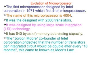
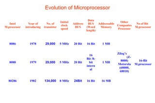
The document discusses the evolution of microprocessors from 1971 to present. It begins with Intel releasing the first microprocessor, the 4-bit 4004, in 1971. The document then outlines the progression from 4-bit to 8-bit to 16-bit and finally 32-bit and 64-bit microprocessors. It provides details on the features of early microprocessors like the 8008, 8080, 8085 and later models like the 8086, 80286, 80386 and Pentium. The number of transistors integrated onto a single chip doubled every 18 months, as predicted by Moore's Law.
PIC A special purpose integrated circuit that function as an overall manager in an interrupt driven system.
It accepts request from the peripheral equipment,determines which of the incoming request is of the highest priority, ascertains whether the incoming request has a higher priority value than the level currently being serviced, and issues an interrupt to the CPU based on this determination.
MPMC UNIT-1. Microprocessor 8085 pdf Microprocessor and MicrocontrollerRAHUL RANJAN
Diploma in Electrical Engineering MICROPROCESSOR AND MICROCONTROLLER UNIT-1 Full Notes 📝 Microprocessor 8085 State Board Of Technical Education [SBTE] BIHAR
Live B tech Projects & Industrial Training @Technogroovy Technogroovy India
like our page for more updates:
https://www.facebook.com/Technogroovyindia
With Best Regard's
Technogroovy Systems India Pvt. Ltd.
www.technogroovy.com
Call- +91-9582888121
Whatsapp- +91-8800718323
all about architecture and memory interfacing. This is the most important lecture for microprocessor.
In computer science you must known about this lecture.
1. 8-Bit Microprocessor:
The 8085 is an 8-bit microprocessor, which means it can process data in 8-bit chunks at a time. This restricts the processor to working with values from 0 to 255.
2. Architecture:
The 8085 microprocessor has a simple architecture consisting of various registers, a control unit, and an arithmetic logic unit (ALU).
It has 74 instructions and 246 opcodes.
3. Registers:
Accumulator (A): Used for performing arithmetic and logic operations.
General-Purpose Registers (B, C, D, E, H, L): Used for various data manipulation tasks.
Stack Pointer (SP): Used to manage the stack.
Program Counter (PC): Keeps track of the address of the next instruction to be executed.
4. Memory:
The 8085 microprocessor can address up to 64KB of memory, which includes RAM (Random Access Memory) and ROM (Read-Only Memory).
Memory is organized into 16-bit addresses.
5. Data and Address Bus:
The 8085 has an 8-bit data bus and a 16-bit address bus, allowing it to communicate with external memory and peripheral devices.7. Instruction Set:
The 8085 uses a Reduced Instruction Set Computer (RISC) architecture with a relatively small instruction set. Instructions are categorized into data transfer, arithmetic and logical operations, control flow, and input/output operations.
8. Addressing Modes:
The 8085 supports various addressing modes, such as direct addressing, immediate addressing, register indirect addressing, and more, allowing for flexible data manipulation.
9. Interrupts:
The 8085 microprocessor features five interrupt lines, which are used for handling external interrupts. It supports both maskable and non-maskable interrupts.
10. Flags:7. Instruction Set:
The 8085 uses a Reduced Instruction
Computer system architecture (microprocessor 8085) unit 4Anjaan Gajendra
Microprocessor: Organization of 8085 microprocessor, Instruction set of 8085, Mnemonics and operation codes
of data transfer group, Arithmetic group, Logic group, Branches group and stack, I/O and Machine control group,
Assembly language, Assembler, Simple programs in assembly language.
Quality defects in TMT Bars, Possible causes and Potential Solutions.PrashantGoswami42
Maintaining high-quality standards in the production of TMT bars is crucial for ensuring structural integrity in construction. Addressing common defects through careful monitoring, standardized processes, and advanced technology can significantly improve the quality of TMT bars. Continuous training and adherence to quality control measures will also play a pivotal role in minimizing these defects.
COLLEGE BUS MANAGEMENT SYSTEM PROJECT REPORT.pdfKamal Acharya
The College Bus Management system is completely developed by Visual Basic .NET Version. The application is connect with most secured database language MS SQL Server. The application is develop by using best combination of front-end and back-end languages. The application is totally design like flat user interface. This flat user interface is more attractive user interface in 2017. The application is gives more important to the system functionality. The application is to manage the student’s details, driver’s details, bus details, bus route details, bus fees details and more. The application has only one unit for admin. The admin can manage the entire application. The admin can login into the application by using username and password of the admin. The application is develop for big and small colleges. It is more user friendly for non-computer person. Even they can easily learn how to manage the application within hours. The application is more secure by the admin. The system will give an effective output for the VB.Net and SQL Server given as input to the system. The compiled java program given as input to the system, after scanning the program will generate different reports. The application generates the report for users. The admin can view and download the report of the data. The application deliver the excel format reports. Because, excel formatted reports is very easy to understand the income and expense of the college bus. This application is mainly develop for windows operating system users. In 2017, 73% of people enterprises are using windows operating system. So the application will easily install for all the windows operating system users. The application-developed size is very low. The application consumes very low space in disk. Therefore, the user can allocate very minimum local disk space for this application.
Saudi Arabia stands as a titan in the global energy landscape, renowned for its abundant oil and gas resources. It's the largest exporter of petroleum and holds some of the world's most significant reserves. Let's delve into the top 10 oil and gas projects shaping Saudi Arabia's energy future in 2024.
Event Management System Vb Net Project Report.pdfKamal Acharya
In present era, the scopes of information technology growing with a very fast .We do not see any are untouched from this industry. The scope of information technology has become wider includes: Business and industry. Household Business, Communication, Education, Entertainment, Science, Medicine, Engineering, Distance Learning, Weather Forecasting. Carrier Searching and so on.
My project named “Event Management System” is software that store and maintained all events coordinated in college. It also helpful to print related reports. My project will help to record the events coordinated by faculties with their Name, Event subject, date & details in an efficient & effective ways.
In my system we have to make a system by which a user can record all events coordinated by a particular faculty. In our proposed system some more featured are added which differs it from the existing system such as security.
Industrial Training at Shahjalal Fertilizer Company Limited (SFCL)MdTanvirMahtab2
This presentation is about the working procedure of Shahjalal Fertilizer Company Limited (SFCL). A Govt. owned Company of Bangladesh Chemical Industries Corporation under Ministry of Industries.
Hybrid optimization of pumped hydro system and solar- Engr. Abdul-Azeez.pdffxintegritypublishin
Advancements in technology unveil a myriad of electrical and electronic breakthroughs geared towards efficiently harnessing limited resources to meet human energy demands. The optimization of hybrid solar PV panels and pumped hydro energy supply systems plays a pivotal role in utilizing natural resources effectively. This initiative not only benefits humanity but also fosters environmental sustainability. The study investigated the design optimization of these hybrid systems, focusing on understanding solar radiation patterns, identifying geographical influences on solar radiation, formulating a mathematical model for system optimization, and determining the optimal configuration of PV panels and pumped hydro storage. Through a comparative analysis approach and eight weeks of data collection, the study addressed key research questions related to solar radiation patterns and optimal system design. The findings highlighted regions with heightened solar radiation levels, showcasing substantial potential for power generation and emphasizing the system's efficiency. Optimizing system design significantly boosted power generation, promoted renewable energy utilization, and enhanced energy storage capacity. The study underscored the benefits of optimizing hybrid solar PV panels and pumped hydro energy supply systems for sustainable energy usage. Optimizing the design of solar PV panels and pumped hydro energy supply systems as examined across diverse climatic conditions in a developing country, not only enhances power generation but also improves the integration of renewable energy sources and boosts energy storage capacities, particularly beneficial for less economically prosperous regions. Additionally, the study provides valuable insights for advancing energy research in economically viable areas. Recommendations included conducting site-specific assessments, utilizing advanced modeling tools, implementing regular maintenance protocols, and enhancing communication among system components.
Student information management system project report ii.pdfKamal Acharya
Our project explains about the student management. This project mainly explains the various actions related to student details. This project shows some ease in adding, editing and deleting the student details. It also provides a less time consuming process for viewing, adding, editing and deleting the marks of the students.
Democratizing Fuzzing at Scale by Abhishek Aryaabh.arya
Presented at NUS: Fuzzing and Software Security Summer School 2024
This keynote talks about the democratization of fuzzing at scale, highlighting the collaboration between open source communities, academia, and industry to advance the field of fuzzing. It delves into the history of fuzzing, the development of scalable fuzzing platforms, and the empowerment of community-driven research. The talk will further discuss recent advancements leveraging AI/ML and offer insights into the future evolution of the fuzzing landscape.
1. Evolution of Microprocessor
The first microprocessor designed by Intel
corporation in 1971 which first 4-bit microprocessor.
The name of this microprocessor is 4004.
It was the designed with 2300 transistors.
It was designed by using large scale integration
(LSI) technology.
It has 640 bytes of memory addressing capacity.
The “Jordon Moore” co-founder of Intel
corporation,pridected that the number of transistors
per integrated circuit would be double after every “18
months", this came to known as Moor’s Law.
2. Evolution of Microprocessor
• Intel Microprocessor is divided into following groups.
1. 4-bit Microprocessor-4004.
2. 8-bit Microprocessor-8008,8080,8085.
3. 16-bit Microprocessor-8086,8088,80286.
4. 32-bit Microprocessor-
80386,80486,pentium.pentium pro,pentium-
II,pentium-III,pentium-IV
3. Evolution of Microprocessor
Intel
M.processor
Year of
introducing
No. of
transistor
Initial
clock
speed
Address
BUS
Data
BUS
(Word
length)
Addressabl
e Memory
Other
Companies
Processor
No of Bit
M.processor
4004 1971 2,300
108
KHz
10 Bit 4 Bit 640 bytes
Rockwell
International
PPS-4-bit
MP
4-Bit
M.processor
8008 1972 3,500
200
KHz
14 Bit 8 Bit 16 Kbytes
Zilog’s
(Z-80,
Z-800)
Motorola’s
(6800,6809)
8-Bit
M.processor
8080 1972 6000
2
MHz
16 Bit 8 Bit 64 Kbytes
8085 1976 6,500
5
MHz
16 Bit 8 Bit 64 Kbytes
4. Evolution of Microprocessor
Intel
M.processor
Year of
introducing
No. of
transistor
Initial
clock
speed
Address
BUS
Data
BUS
(Word
length)
Addressable
Memory
Other
Companies
Processor
No of Bit
M.processor
8086 1978 29,000 5 MHz 20 Bit 16 Bit 1 MB
Zilog’s
(Z-
8000)
Motorola
(68000,
68010)
16-Bit
M.processor
8088 1979 29,000 5 MHz 20 Bit
16
Bit /8-
bit
intern
al
1 MB
80286 1982 134,000 8 MHz 24Bit 16 Bit 16 MB
5. Evolution of Microprocessor
Intel
M.processor
Year of
introducing
No. of
transistor
Initial
clock
speed
Address
BUS
Data
BUS
(Word
length)
Addressable
Memory
Other
Companies
Processor
No of Bit
M.processor
80386 1985 2,75,000
16
MHz
32Bit 32 Bit 4 GB
Zilog’s
(Z-80000)
Motorola
(68020,
68030)
32-Bit
M.process
or
80486 1989
1.2
Million
25
MHz
32 Bit 32 Bit 4 GB
Pentium 1993
3.1
Million
60
MHz
32 Bit 32 Bit 4 GB
Pentium-
Pro
1995
5.5
Million
150
MHz
32 Bit 32 Bit 64 GB
6. 8085 Microprocessor
Introduction:-The microprocessor is the central processing
(CPU) of microcomputer.
It is also known heart of computer or Brain of computer.
It designed on single chip or IC (Integrated circuit).
Microprocessor is also known as programmable digital
device, designed with registers, flip-flop and timing
element.
It is also defined as multipurpose,programmable,clock
driven, register based electronic device, that reads the
instructions from storage device called memory, accepts
the binary data as input & process the data according to
instructions & provide the result.
7. 8085 Microprocessor
• The Intel 8085 is the 8-bit microprocessor
developed by Intel corporation in year 1976.
• It known as 8-bit Microprocessor because it can
process 8-bits at a time.
• If the processor consists of more than 8-bits the
processor takes up 8-bits of data at first & makes its
processing, then next group of data taken up one
by one.
8. Features of 8085 Microprocessor
1.Intel 8085 is 8 bit microprocessor.
2.It is developed by Intel corporation in 1976.
3.It has 40 pins IC (Integrated circuit ) fabricated on
single chip.
4.Its clock speed is 3 to 5 MHz.
5.The Intel 8085 uses a single +5 V D.C. supply for
its operation.
6.It is designed by using 6200 to 6500.
7.It has 8-bit data Bus.
8.It has 16 bit address.
9. Features of 8085 Microprocessor
9.It has16 bit address lines, therefore it can access
16
2 = 64 Kbytes of memory locations.
10.It has 8-bit I/O Addresses,
8
2 = 256 (0---255) ports can be accessed.
11. It has 80 basic instructions & 246 opcodes.
Note : opcode means operational codes every instruction having a
code which is stored in memory.
MVI A,05 is instruction, the meaning of this instruction is to transfer
05 data in to accumulator.
MVI A ,05 ( in coded form 3E,05) where 3E is the opcode of
instruction & 05 is 8-bit data)
10. Pin Diagram & Description of 8085 Microprocessor
VSS AD0-AD7
Vcc
X1
X2 A8-A15
RESET IN CLK
RESET OUT HOLD
IO/M HLDA
S0 TRAP
S1 RST 7.5
RD RST 6.5
WR RST 5.5
ALE INTR
SID
SOD INTA
READY
INTEL
8
0
8
5
11. Pin Diagram & Description of 8085 Microprocessor
The 8085 microprocessor has 40 pin IC.
Pin configuration is as follow.
1.AD0 –AD7 :This is the multiplexed &
bidirectional Bus.
It is used as address as well as data Bus.
The lower 8-bits address (A0—A7) is multiplexed
with data Bus (D0—D7).
2.A8- A15 : This is higher order Bus ,higher order
addresses (A8-A15) sending through this bus
It 8 bit higher order or most significant bits
(A8-A15) sending on this bus.
12. Pin Diagram & Description of 8085 Microprocessor
3.ALE : (Address latch Enable) Output
It is active high signal.
It controls the multiplexed bus AD0-AD7.
When ALE goes high the Bus AD0-AD7 is used as address Bus
i.e. (A0-A7).
When ALE goes low the Bus AD0-AD7 is used as data Bus.
4. IO/M (output pin) :
It is status signal which distinguishes whether the address is for
memory or I/O.
When it goes high address on the address bus is for I/O
IO/M = High -- Address for I/O
IO/M = Low -- Address for Memory
13. Pin Diagram & Description of 8085 Microprocessor
S0 /S1 (output) :These are status signal sent by the
microprocessor to distinguish various types of operation given in
table.
S1 S0 Operations
0 0 HLT
0 1 WRITE
1 0 READ
1 1 FETCH
RD (Output) : This signal is used to control READ operation.
When it goes low the memory or I/O device is read.
WR ( Output) : This signal is used to control WRITE operation
When it goes low data is written into the selected memory or
I/O .
14. Pin Diagram & Description of 8085 Microprocessor
READY (Input): This signal is used by microprocessor to check
peripheral is ready to transfer the data or not.
A slow peripherals may be connected through this line or pin.
HOLD (Input) : Another devices or I/O devices requesting to the
processor for the use of data & address Bus.
HLDA (Output) : Acknowledgement
This is acknowledgement pin .
The processor sends acknowledgement (permission) to the
requesting device that processor is ready to accept the request.
15. Pin Diagram & Description of 8085 Microprocessor
INTR (Interrupt) Input :
It is an interrupt request signal.
INTA (Output): If processor is ready to accept the
request then sends acknowledgement signals.
Note :Interrupts are signals that cause the computer’s
CPU to suspend what is to be doing & transfer to
special program called Interrupt handler.
When interrupt signal occurs at that time processor
stops his main program & transfer towards special
programs, the processor executes this subprogram
given by interrupt signals & returns towards main
program.
16. Pin Diagram & Description of 8085 Microprocessor
RST 7.5,RST 6.5,RST 5.5 and TRAP :
These interrupt signals.
Other peripheral devices or co-processors interrupt through this
signals or pins.
TRAP has highest priority.
RESET IN : This is active low signal used to reset
microprocessor.
When this signal is received by the
microprocessor,miroprocessor clears program counter i.e. 0000.
RESET OUT (Output): It is active high output signal.
It indicates that processor is being reset.
17. Pin Diagram & Description of 8085 Microprocessor
• X1,X2 (Input) :These are clock input pins connected
to crystal oscillator
• Which drives an internal circuit of microprocessor to
produce suitable clock, for operation of the
microprocessor.
• CLK (Output):
• It is clock output for user can be used for other digital
IC’s.
• It’s frequency is same at which processor operates.
• Internal operating frequency of microprocessor is
available on this pin & used to operate other devices
in the system with speed.
18. Pin Diagram & Description of 8085 Microprocessor
• SID & SOD :Serial input data & serial output data
• SID pin is used to accept one bit data under software
control.
• VCC : Vcc provides +5v supply for the operation of
microprocessor.
• VSS : Ground reference.
19. 8085 Microprocessor Architecture or Block diagram of 8085
• The Block diagram of Intel 8085 consists of following
three main sections.
• 1.Arithematic and Logic unit (ALU)
• 2.Timing & control unit
• 3.Set of Registers
20. 8085 Microprocessor Architecture or Block diagram of 8085
INTR,RST 7.5,RST 6.5,RST 5.5 ,TRAP SID SOD
INTA
Interrupt control Serial
input/output
ACCUMULATOR
TEMP.
REGISTER
FLAG
REGISTER
ALU
TIMING & CONTROL
INSTRN
REGISTER
INSTRN
DECODER
& M/C CYCLE
ELCODING
ADDRESS
BUFFER
ADDR./
DATA
BUFFER
W Z
B C
D E
H L
Stack Pointer
Prog. Counter
Incr./Decre
Addr.Latch
A15-A8
AD7-AD0
21. 8085 Microprocessor Architecture or Block diagram of 8085
• 1.Airtematic & Logic control : (ALU)
• ALU is the main part of microprocessor which
performs arithmetic & logic operations
• Arithmetic operation like addition subtraction.
• The logical operations like
AND,OR,NOT,Increment,decrement,shift,rotate.
• It takes data from accumulator & temporary
register & stores the result in accumulator.
• ALU is combinational circuit which consists of
adder, AND gate, OR gate & NOT gate.
22. 8085 Microprocessor Architecture or Block diagram of 8085
• 2.Timing and control Unit :-
• The timing & control unit is section of CPU.
• It generates timing & control signals which are necessary
for the execution of instructions.
• It controls data flow between CPU & peripherals (including
memory ).
• It performs data transfer & decision making operations.
• It consists of instruction register, instruction decoder,
timing & control circuit.
• It control entire operation of microprocessor & peripherals
connected to it.
23. 8085 Microprocessor Architecture or Block diagram of 8085
• 3.Register Organisation:Resgisters are used by
microprocessor for temporary storage of data & instructions.
• These registers are known internal memory of M.processor.
• The 8085 has following registers :-
• 1] One 8-bit accumulator (ACC) or Reg. A
• 2] Six 8-bit general purpose registers these are B,C,D,E,H,L.
• 3] One 16-bit stack pointer (SP)
• 4] One 16-bit program counter (PC)
• 5] Instruction register
• 6.Temporary Register
24. 8085 Microprocessor Architecture or Block diagram of 8085
• 1] One 8-bit accumulator (ACC) or Reg. A :-
• Accumulator is 8-bit registers.
• It is also known as Reg.A.
• It is used to hold one of the operand (data) of an
arithmetic & logical operation.
• The another operand (Data) for arithmetic & logical
operations may stored in memory or one of the
register.
• It is used as input device to ALU.
• Finally result is stored in the accumulator.
25. 8085 Microprocessor Architecture or Block diagram of 8085
• 2] General purpose registers :-
• The 8085 has 6 general purpose 8 bit registers
B,C,D,E,H,L.
• These registers available for the user.
• These registers used to store 8-bit data.
• The pair of two registers can be used as 16-bit
registers these pairs are BC,DE,HL.
26. 8085 Microprocessor Architecture or Block diagram of 8085
• 3] Stack pointers (SP) :-
• It is special purpose register.
• It is used to access stack memory.
• It always used to point to the stack memory.
Note :-Stack Memory : The stack is a sequence of memory
locations set aside by programmer to store the contents of
accumulator,flags,program counter,& general purpose
Reg.during execution of program.
• Some part of RAM memory is used as stack.
• During the execution of the program some times it becomes
necessary to save contents of some registers which are
need for some other operations,in subsequent steps of the
program.
• The contents of such registers saved in the stack.
27. 8085 Microprocessor Architecture or Block diagram of 8085
• 4.Program counter : (PC)
• Program counter is 16-bit special purpose Register.
• It is always used to hold the address of program
memory.
• It gives the track of memory addresses of the
instructions in the program while they are being
executed.
• It never hold operands or data
• It is automatically incremented by control unit during
instruction fetch operations.
• During instruction fetch operation a 8085
microprocessor places contents of PC on address bus
to select appropriate location of program memory.
28. 8085 Microprocessor Architecture or Block diagram of 8085
• 5.Instruction Register :-
• The instruction register holds the opcode (Operation
code or instruction code ) of the instruction which
being decoded & executed.
• It is 8-bit register.
• It is not available for user.
• 6] temporary Register :-
• It is 8-bit register associated with temporary.
• It is not available for user.
• It holds data during an arithmetic / Logical Operation
• It is used by the microprocessor.
29. 8085 Microprocessor Architecture or Block diagram of 8085
• Flag Register :-
• It is available for user.
• The ALU stores the status of result in the flag
registers.
• The ALU includes five flip-flops which are set or reset
after an operation according to condition of result.
• These flag registers are known as flags.
• There are five flags of 8085 M.processor. ( carry
flag,Auxillary carry flag, parity flag, Zero flag, sign flag )
• These flag registers are connected to ALU.
30. 8085 Microprocessor Architecture or Block diagram of 8085
• Flag structure of 8085 or Program status word of 8085
MSB LSB
Zero Flag Parity Flag Carry Flag
• Sign Flag Auxillary Carry Flag
D7 D6 D5 D4 D3 D2 D1 D0
S Z X AC X P X CY
31. 8085 Microprocessor Architecture or Block diagram of 8085
• 1] Carry Flag ( CY or CF) :-
• After execution of instruction carry is generated ,carry flag
set to ‘1’ otherwise reset to ‘0’.
• 2] Auxillary carry Flag (AC) :-
• If carry is generated from bit 3 to bit 4 (D4-D3) ,it is set to
‘1’ otherwise reset to ‘0’.
• 3] Parity Flag (P) :-
• If result of operation contains even number of ‘1’ the parity
flag is set to’1’ ,or result of operation contains odd no.of
‘1’,the parity flag reset to ‘0’.
32. 8085 Microprocessor Architecture or Block diagram of 8085
• 4] Zero Flag :-
• If result of operation is zero (0), then zero flag is set
to ‘1’ otherwise non zero result reset to ‘0’.
• 5] Sign Flag (S) :-
• The sign flag ‘S’ set to 1 ,if the result of operation is
negative.
• It is always used in signed arithmetic operation.
• In logical operation MSB is 1 the sign flag is set to1.
33. 8085 Microprocessor Architecture or Block diagram of 8085
• Applications of microprocessor :-
• 1.Microprocessor are used in controllers, personal
computers, low to moderate speed data
communication.
• 2. microprocessor used as digital controller to control
some physical parameters like temperature, pressure.
• 3.It is used to control motor speed, traffic light
controller, conveyer controls, stepper motor controller.
• 4.It is used in data communication application
applications including data processing error detection,
serial to parallel & parallel to serial data transfers.
34. 8085 Microprocessor Architecture or Block diagram of 8085
• 5.It is used in personal computer.
• 6.Microprocessor are also used in automobils,applications
are ignition control, automatic fuel control.
• 7.Microprocessors are used in many medical instruments
like X-ray machines,ECG machines.
8.Microprocessors are used in testing & measuring
instruments, applications are CRO’s,signal generator
power supplies, spectrum analyzers.
35. 8085 Microprocessor Architecture or Block diagram of 8085
• Limitations of 8-Bit microprocessor:-
• 1.The word length is 8-bit hence processing speed is low.
• 2.Due to 16-bit address lines, we can address only up to 64
Kbytes of memory.
• 3.8-bit microprocessor has multiplexed address & data bus,
so extra hardware is required to separate address signals.
• 4.It can read one instruction at a time ,unless first
instruction gets executed completely, microprocessor can
not read second instruction from memory as it has only one
instruction register.
• 5.Operating speed is less so the speed of execution is low.
36. 8085 Microprocessor Architecture or Block diagram of 8085
• 6.Using 8-bit microprocessor, we can not design
multiprocessor system.
• 7. Due to limited size of the all register, we can store
limited data bytes in the microprocessor memory.
• 8.There is no memory management unit.
• 9. It is used for control applications.
• 10. It is not used in work stations & servers.