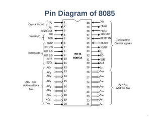
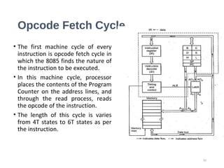
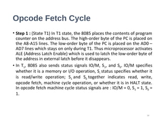
The document provides information about the pin diagram of the 8085 microprocessor. It describes the various pins including:
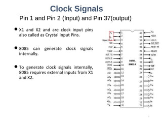
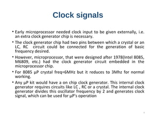
1. Clock input pins X1 and X2 which are used to generate internal clock signals.
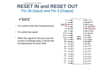
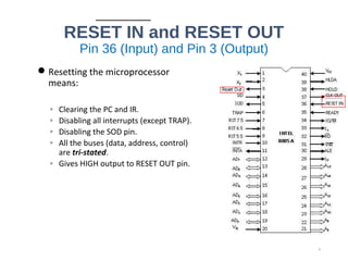
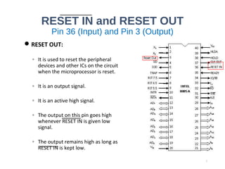
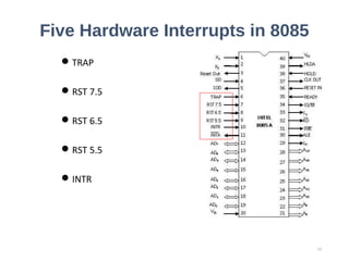
2. RESET IN pin which is used to reset the microprocessor and RESET OUT pin which outputs a reset signal.
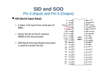
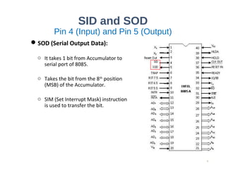
3. Serial I/O pins SID and SOD which are used for serial data input and output.
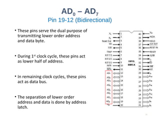
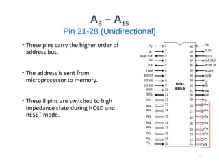
4. Address and data bus pins including A8-A15 for higher order address and AD0-AD7 which serve as both the lower order address and data bus.
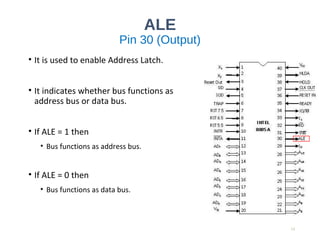
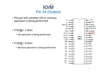
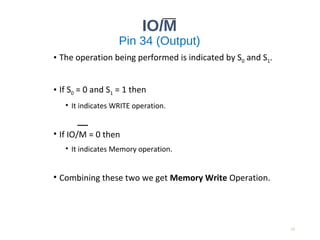
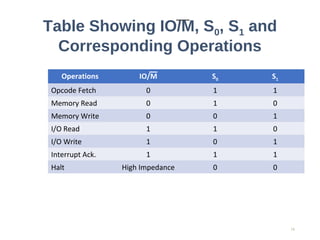
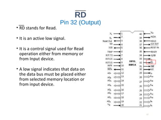
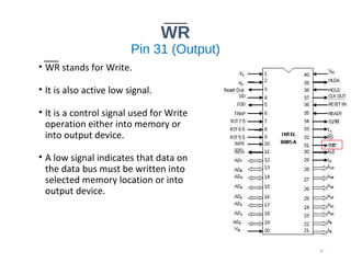
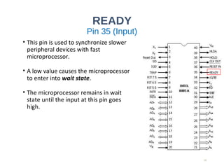
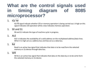
Control signal pins such as IO/M, ALE, RD,